3/8
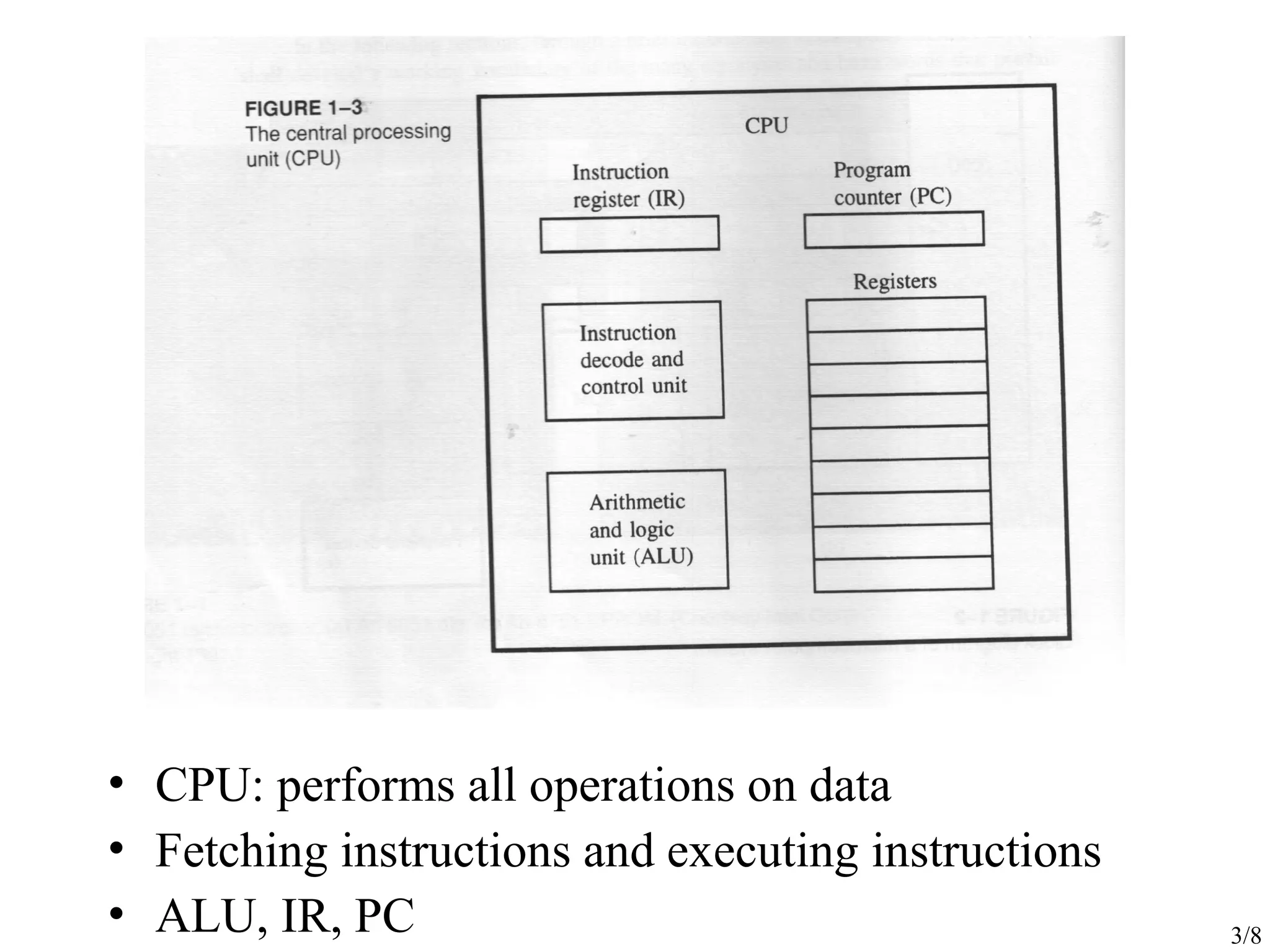
• CPU: performsall operations on data
• Fetching instructions and executing instructions
• ALU, IR, PC
4.
4/8
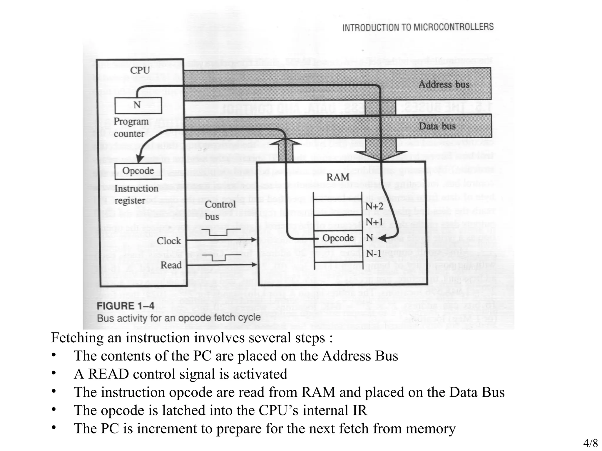
Fetching an instructioninvolves several steps :
• The contents of the PC are placed on the Address Bus
• A READ control signal is activated
• The instruction opcode are read from RAM and placed on the Data Bus
• The opcode is latched into the CPU’s internal IR
• The PC is increment to prepare for the next fetch from memory
5.
5/8
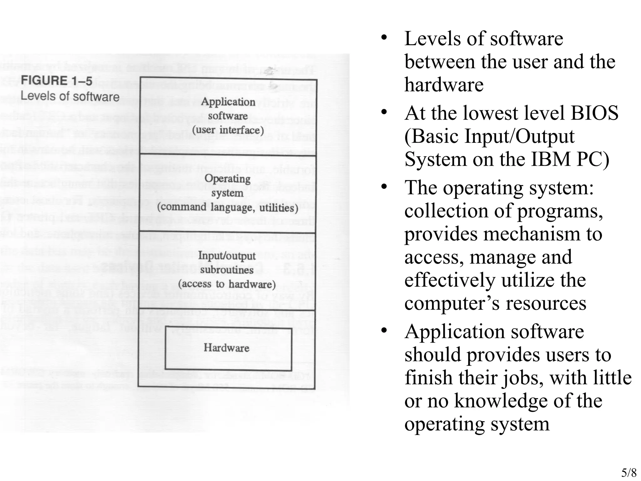
• Levels ofsoftware
between the user and the
hardware
• At the lowest level BIOS
(Basic Input/Output
System on the IBM PC)
• The operating system:
collection of programs,
provides mechanism to
access, manage and
effectively utilize the
computer’s resources
• Application software
should provides users to
finish their jobs, with little
or no knowledge of the
operating system
6.
6/8
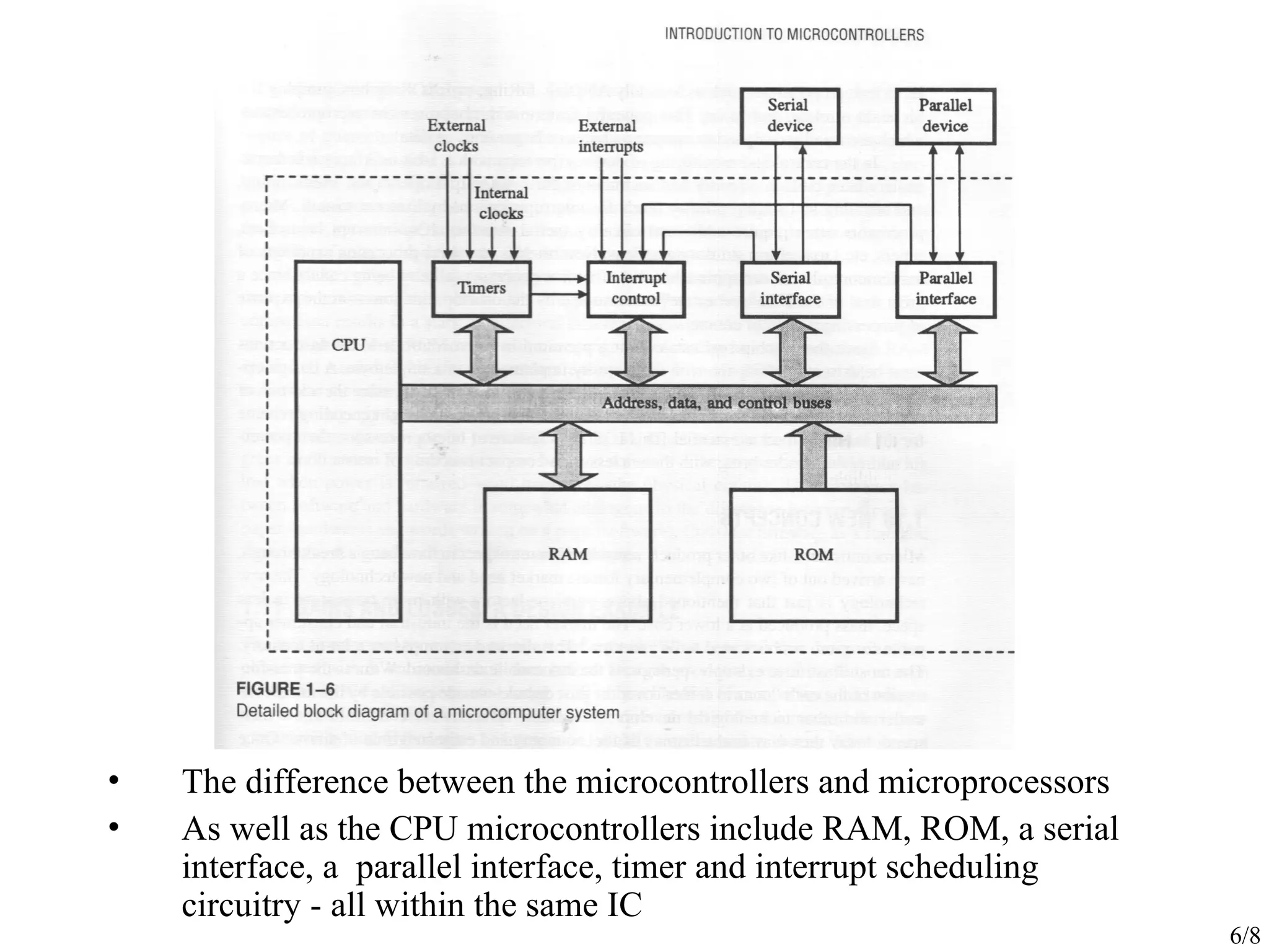
• The differencebetween the microcontrollers and microprocessors
• As well as the CPU microcontrollers include RAM, ROM, a serial
interface, a parallel interface, timer and interrupt scheduling
circuitry - all within the same IC
7.
7/8
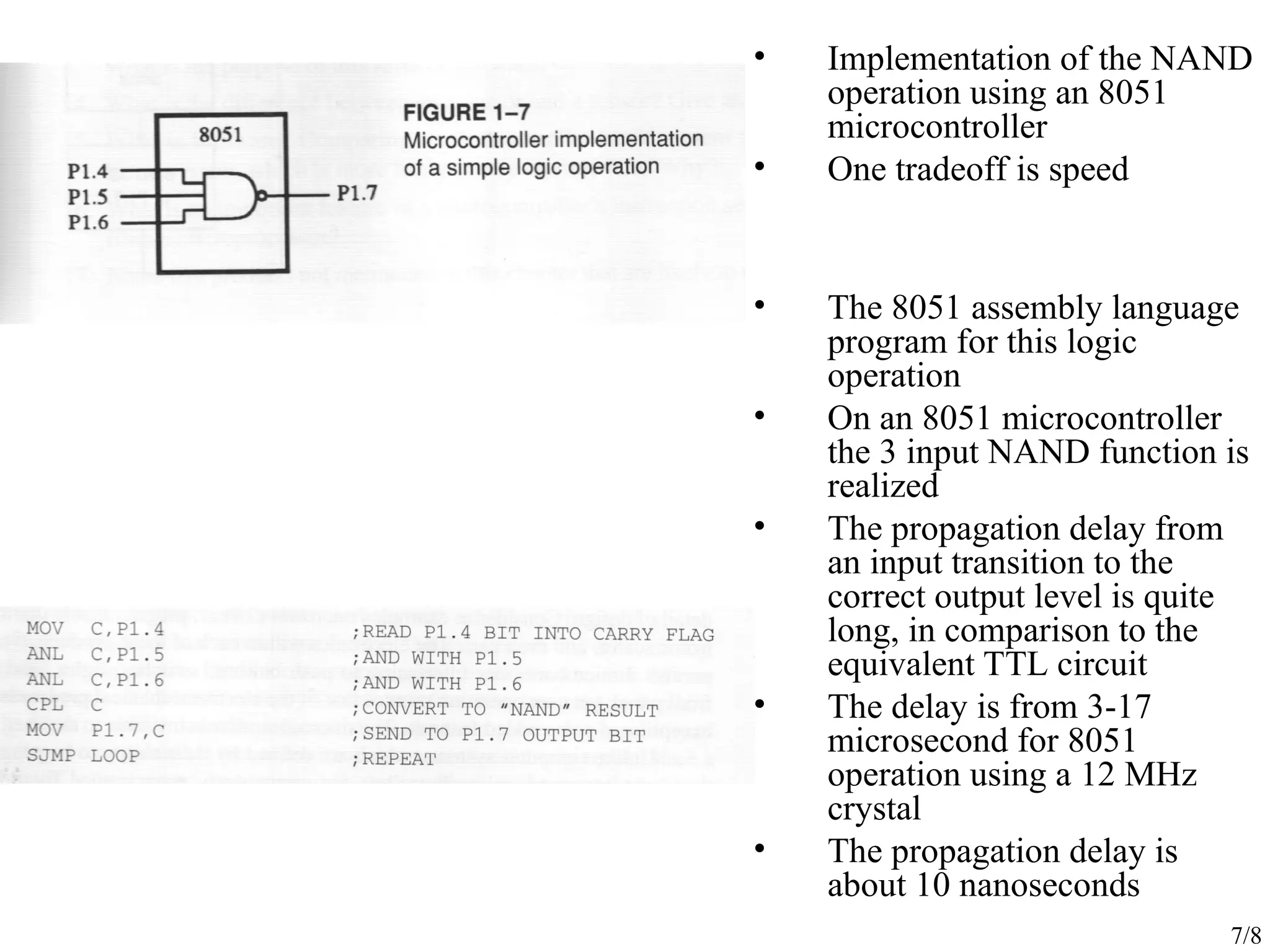
• Implementation ofthe NAND
operation using an 8051
microcontroller
• One tradeoff is speed
• The 8051 assembly language
program for this logic
operation
• On an 8051 microcontroller
the 3 input NAND function is
realized
• The propagation delay from
an input transition to the
correct output level is quite
long, in comparison to the
equivalent TTL circuit
• The delay is from 3-17
microsecond for 8051
operation using a 12 MHz
crystal
• The propagation delay is
about 10 nanoseconds
8.
8/8
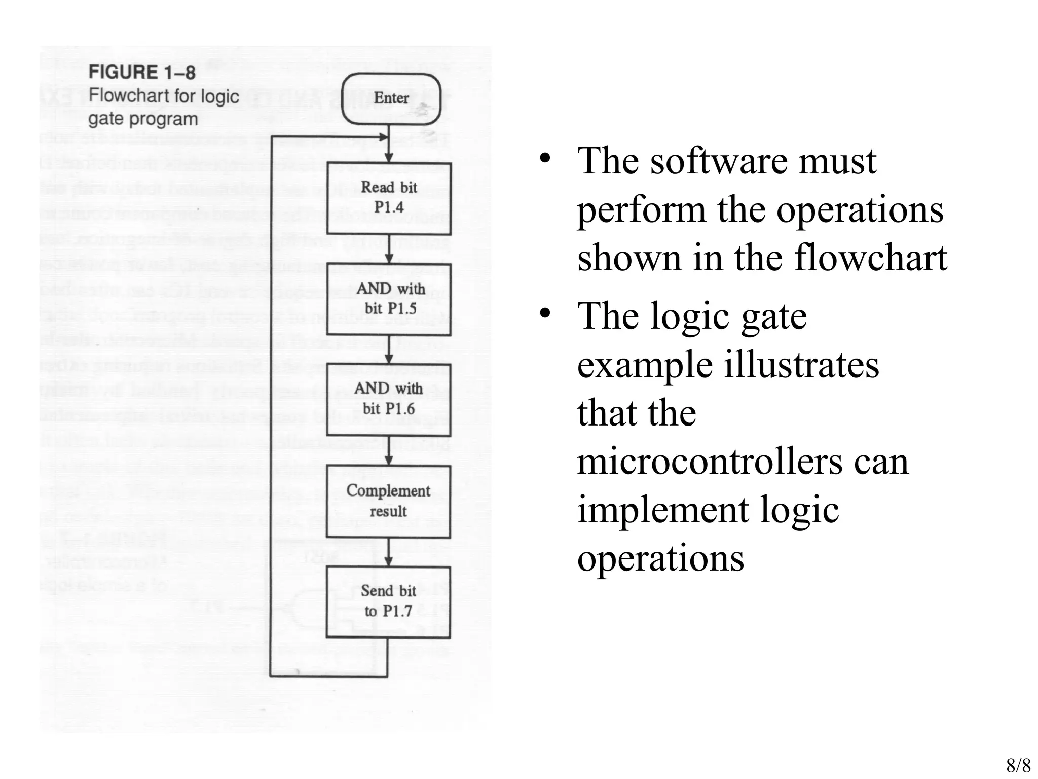
• The softwaremust
perform the operations
shown in the flowchart
• The logic gate
example illustrates
that the
microcontrollers can
implement logic
operations