Download as PDF, PPTX

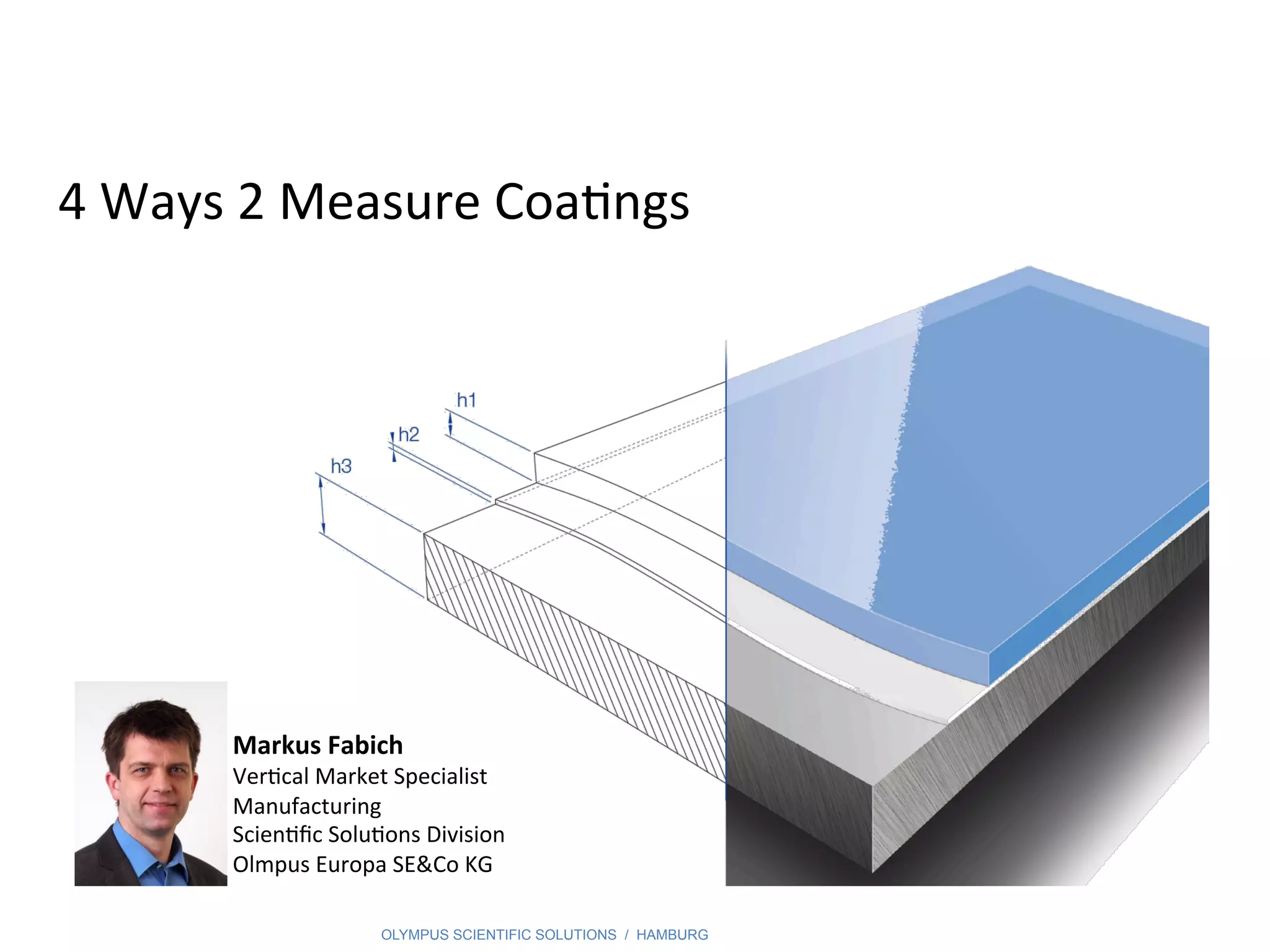
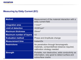
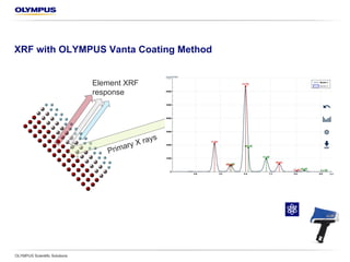
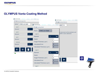
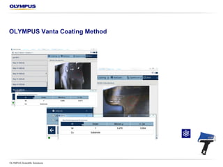
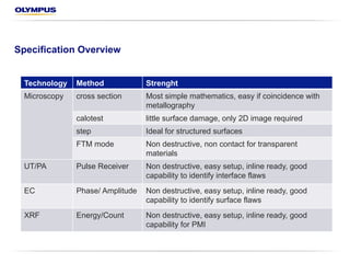
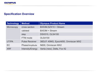


The document discusses various methods to measure coating thickness, emphasizing the importance of measurement for functionality and monitoring purposes. It outlines different technologies such as microscopy, ultrasound, eddy current, and XRF, detailing their capabilities, detection limits, and application contexts. The session aims to guide the selection of appropriate measurement techniques based on specific needs, providing an overview of technology strengths and limitations.