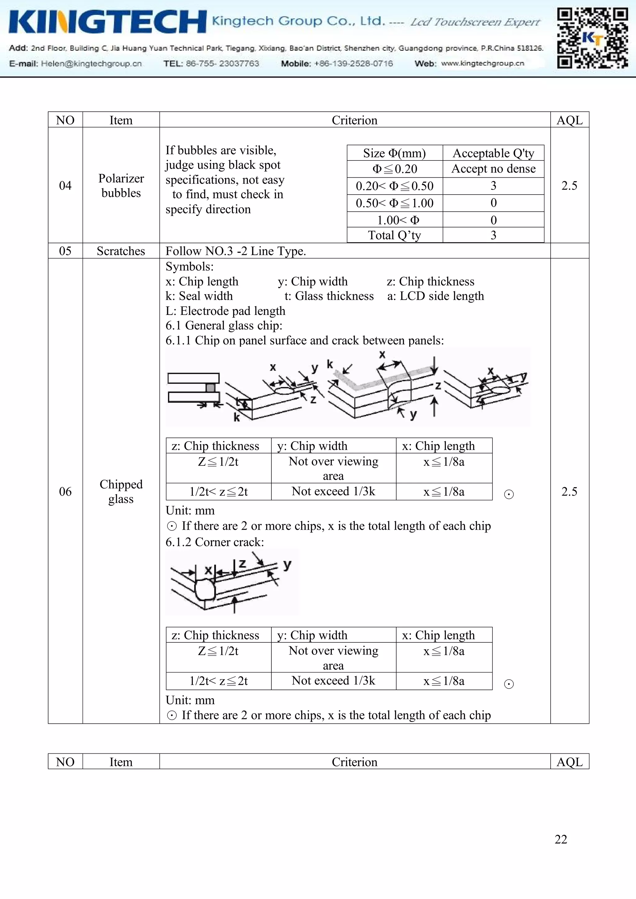
Download to read offline
![6
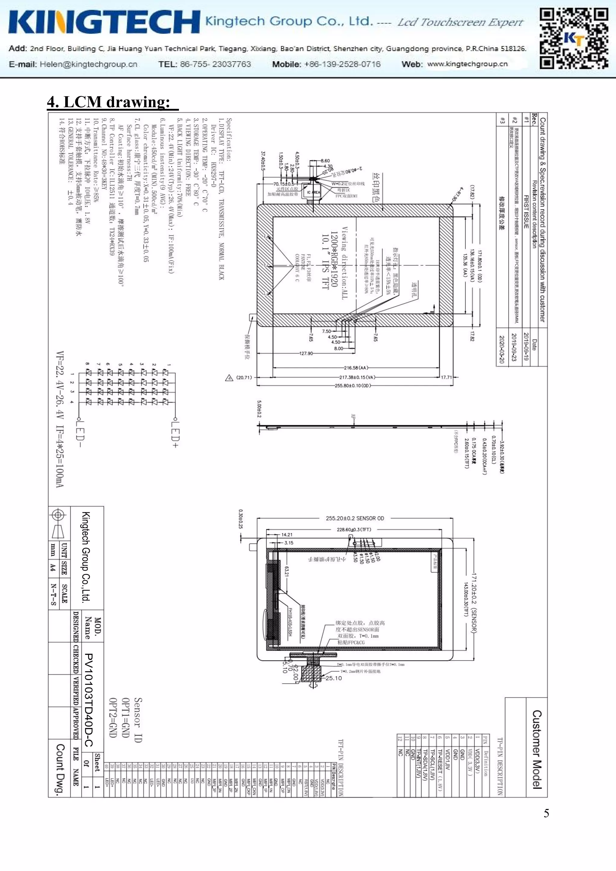
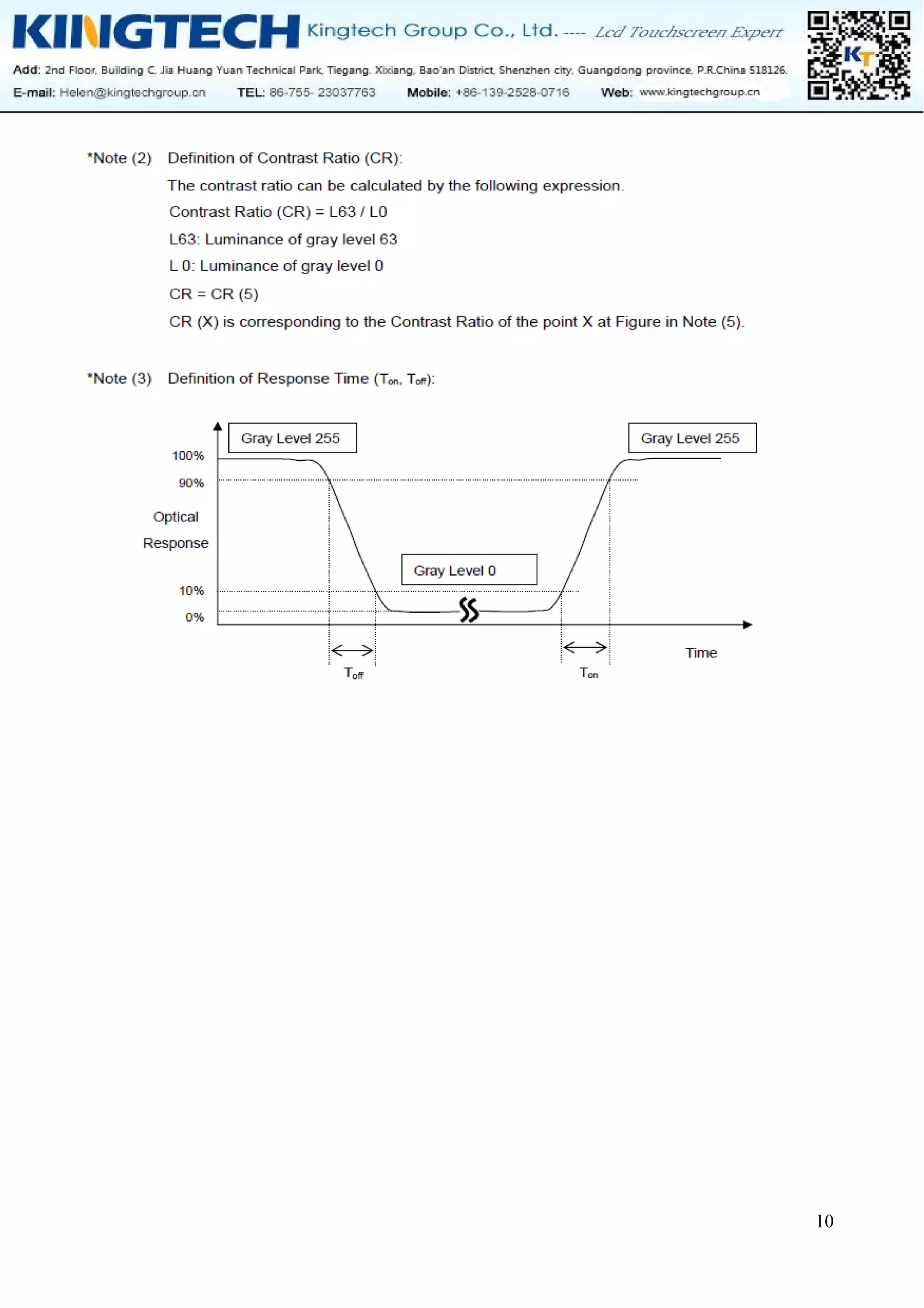
5. Electrical Characteristics
5-1 Absolute Maximum Ratings (Ta=25℃ VSS=0V)
Item Symbol Min. Type Max. Unit Remark
Input Voltage VCI-VSS -0.3 - +3.9 Volt Note1
Supply Voltage VDDIO-VSS -0.3 - +3.6 Volt Note1
Operating Temperature Topr -10 - +50 ℃ -
Storage Temperature Tstg -20 - +60 ℃ -
Note1: Absolute maximum rating is the limit value beyond which the IC maybe broken.
They do not assure operations.
5-2 Operating Conditions
(VDD=2.8 ~ 3.3V, TA=-40 ~ 85 C)
Parameter Symbol Test condition
Spec.
Unit Note
Min. Typ. Max.
Input high voltage VIH VDD= 2.8 ~ 3.3V 0.7 VDD1 - VDD1 V -
Input low voltage VIL 0 - 0.3 VDD1 V -
VPP
VIH
VPP 8.0 8.25 8.5
V
(1)
VIL V
Output high voltage
(SDO, CABC_PWM_OUT)
VOH1 IOH = -1.0 mA 0.8 VDD1 - VDD1 V -
Output low voltage
(SDO, CABC_PWM_OUT)
VOL1
VDD= 1.7 ~ 2.0V
IOL = 1.0 mA
0 - 0.2 VDD1 V -
Logic High level input current
IIH
VSYNC, HSYNC - - 1 uA -
RESX, DCX, CSX, SCL - - 1 -
IIHD
DB[23:0], SDI, DCX - - 1 uA -
DB[23:0] - - 1
Logic Low level input current
IIL
VSYNC, HSYNC -1 - - uA -
RESX, DCX, CSX, SCL -1 - - -
IILD
DB[23:0], SDI, DCX -1 - - uA
DB[23:0] -1 - - -
Current consumption
standby mode (VDD3-VSSA)
IST(VDD)
VDD3/HS_VCC=2.8V,
VDD1=1.8V
TA =25C
(DSI Ultra Low Power mode)
- -- TBD A -
Current consumption
standby mode
( VDD1– VSSD)
IST(VDD1) - -- TBD A -
Current consumption
standby mode which include
HS_VCC
( HS_VCC-HS_VSS)
IST(VDD1) - -- TBD A -
Oscillator tolerance △ OSC TA =25°
C -5 - 5 % -](https://image.slidesharecdn.com/10-220310053511/75/10-1-inch-1200x1920-mipi-interface-ips-lcd-module-6-2048.jpg)


The document is a specification for the LCD module model PV10103TD40D-C, detailing its general specifications, electrical characteristics, optical characteristics, interface pin assignments, and reliability standards. It includes information on revision history, packing, and quality assurance, emphasizing the importance of thorough testing and adherence to standards for optimal product quality. Various tests and criteria for non-conformities and inspections are outlined to ensure consistency and reliability in production.


