1. Smart Card Tutorial - Part 1
First Published in September 1992
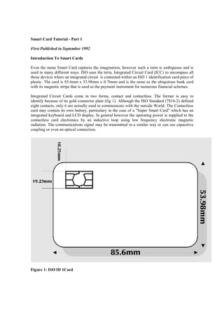
Introduction To Smart Cards
Even the name Smart Card captures the imagination, however such a term is ambiguous and is
used in many different ways. ISO uses the term, Integrated Circuit Card (ICC) to encompass all
those devices where an integrated circuit is contained within an ISO 1 identification card piece of
plastic. The card is 85.6mm x 53.98mm x 0.76mm and is the same as the ubiquitous bank card
with its magnetic stripe that is used as the payment instrument for numerous financial schemes.
Integrated Circuit Cards come in two forms, contact and contactless. The former is easy to
identify because of its gold connector plate (fig 1). Although the ISO Standard (7816-2) defined
eight contacts, only 6 are actually used to communicate with the outside World. The Contactless
card may contain its own battery, particulary in the case of a "Super Smart Card" which has an
integrated keyboard and LCD display. In general however the operating power is supplied to the
contactless card electronics by an inductive loop using low frequency electronic magnetic
radiation. The communications signal may be transmitted in a similar way or can use capacitive
coupling or even an optical connection.
Figure 1: ISO ID 1Card
2. The Contact Card is the most commonly seen ICC to date largely because of its use in France and
now other parts of Europe as a telephone prepayment card.. Most contact cards contain a simple
integrated circuit although various experiments have taken place using two chips. The chip itself
varies considerably between different manufacturers and for a whole gambit of applications. Let
us consider first the purpose for the 6 contacts used by the ICC (fig 2)
3. Figure 2: ISO 7816-2 Connector
Vcc is the supply voltage that drives the chips and is generally 5 volts. It should be noted
however that in the future we are likely to see a move towards 3 volts taking advantage of
advanced semiconductor technology and allowing much lower current levels to be consumed by
the integrated circuit. Vss is the substrate or ground reference voltage against which the Vcc
potential is measured. Reset is the signal line that is used to initiate the state of the integrated
circuit after power on.This is in itself an integral and complex process that we shall describe later
in more detail.
The clock signal is used drive the logic of the IC and is also used as the reference for the serial
communications link. There are two commonly used clock speeds 3.57 MHZ and 4.92 MHZ. The
lower speed is most commonly used to date in Europe but this may change in the future. One may
be tempted to ask why these strange frequencies were chosen, why not just a straight 5 MHZ. The
reason lies in the availability of cheap crystals to form the clock oscillator circuits. Both of these
frequencies are used in the television world for the colour sub carrier frequency. The PAL system
operates using 4.92 MHZ whilst the 3.57 MHZ is used by the American NTSC standard. The the
Vpp connector is used for the high voltage signal that is necessary to program the EPROM
memory. Last, but by no means least is the serial input/output (SIO) connector. This is the signal
line by which the chip receives commands and interchanges data with the outside world. This is
also a fairly complex operation and will be the subject of a more detailed discussion where
symbols such as T0 and T1 will be fully explained.
So what does the chip contain, well the primary use of the IC card is for the portable storage and
retrieval of data. Hence the fundamental component of the IC is a memory module. The following
list represents the more commonly used memory types,
4. T ROM
T PROM
T EPROM
T EEPROM
T RAM
Read only memory (mask ROM)
Programmable read only memory
Erasable programmable ROM
Electrically erasable PROM
Random access memory
A particular chip may have one or more of these memory types. These memory types have
particular characteristics that control their method of use. The ROM type of memory is fixed and
can not be changed once manufactured by the semiconductor company. This is a low cost
memory, in that, it occupies minimum space on the silicon substrate. The use of the silicon is
often referred to as real estate because clearly one wants to get as much as possible into the
smallest possible space. The snag however is that it can not be changed and takes several months
to be produced by the semiconductor company. There is also effectively a minimum order
quantity in order to achieve this low cost.
In order of increasing real estate the PROM comes next. This memory is programmable by the
user through the use of fusible links. However high voltage and currents are required for the
programming cycle and such devices are not normally used in Integrated Circuit Cards. The
EPROM has been widely used in the past but the name for this application is something of a
misnomer. Whilst the memory is erasable, by means of ultra violet light, the necessary quartz
window is never available in the ICC and the memory is really used in one time programmable
mode (OTP). Getting pretty heavy in real estate terms is the EEPROM. This memory is indeed
erasable by the user and can be rewritten many times (between 10,000 and 1,000,000 in a typical
implementation) All of these memories describe so far are non volatile. In other words when the
power is removed they still retain their contents. The random access memory (RAM) is a
different kettle of fish, this is volatile memory and as soon as the power is removed the data
contents is lost.
In order to pursue our studies further we must note that the cost of the IC at saturation (i.e when
development costs have been recouped) is proportional to the square area of silicon used
(assuming constant yield). The ISO connector is so designed to constrain the silicon die size to
about 25mm2 (although it is possible to handle 35mm2 or more). However the important point is
more concerned with reliability where clearly the larger die will be more prone to mechanical
fracture. There is another bi- product that we will consider later where the cost of testing and
personalisation are considerable altered by the complexity of the particular chip. It is clear
however that we should attempt to minimise the contents of the chip on both cost and reliability
grounds commensurate with the particular application .
Well of course you can't have something for nothing and although a telephone card may operate
with a little EEPROM memory (128 - 512 bytes) and the memory control logic, more
sophisticated applications will demand ROM, EEPROM, RAM and a CPU (Central Processing
Unit) to achieve the necessary business. It is the addition of the CPU or micro-controller that
really leads to the term "Smart" although we will not be rigorous in our use of the term.
The control logic should not be overlooked as this is necessary not only for communication
protocols but also to offer some protection of the memory against fraudulent use. The ICC is
probably the security man's dream because unlike most electronic storage and processing devices
it has security intrinsically built in. The ICC really does provide a tamper resistant domain that is
difficult to match with the some what larger security boxes that handle cryptographic processes.
So now we can differentiate the different types of ICC by their content,
5. T Memory only
T Memory with security logic
T Memory with CPU
The security logic can be used to control access to the memory for authorized use only. This is
usually accomplished by some form of access code which may be quite large (64 bits or more).
Clearly the use of EEPROM memory must be strictly controlled where fraudsters can obtain a
financial advantage by unauthorized use. This applies as much to telephone cards as applications
using ICC for cryptographic key carriers. The security advantage of the CPU device is of course
more significant because the CPU is capable of implementing cryptographic algorithms in its own
right, but we will discuss this in more detail in due course.
In the Smart Card world the term application is widely used to describe the software or programs
that the IC implements. In the simplest case the application may be just a file manager for
organising the storage and retrieval of data. Such an application may be totally implemented in
the logic of the chip. Similarly the chip must contain the communications logic by which it
accepts commands from the card acceptance device (CAD) and through which it receives and
transmits the application data. The ICC which contains a CPU can handle more sophisticated
applications and even multi applications since the CPU is also capable of processing the data and
taking decisions upon the various actions that may be invoked. The subject of mult applications
and particulary the implementation of security segregation is another subject for more detailed
discussion in subsequent parts.
6. Smart Card Tutorial - Part 2
First Published in October 1992
How the IC card is made
The manufacture of a smart card involves a large number of processes of which the embedding of the chip
into the plastic card is key in achieving an overall quality product. This latter process is usually referred to as
card fabrication. The whole operation starts with the application requirements specification. From the
requirements individual specifications can be prepared for the chip, card, mask ROM software and the
application software. The ROM software is provided to the semiconductor supplier who manufactures the
chips. The card fabricator embeds the chip in the plastic card. It is also quite normal for the fabricator to load
the application software and personalisation data. Security is a fundamental aspect in the manufacture of a
smart card and is intrinsic to the total process. However we will consider security separately in subsequent
articles in this series. We will look at each of the stages in the manufacture of the smart card as shown in
figure. 1.
1
7. Figure 1: Stages in the manufacture of a Smart Card
Chip specification
There are a number of factors to be decided in the specification of the integrated circuit for the smart card.
For the purpose of this discussion we will consider a CPU based card although the manufacture of a memory
card is substantially a subset of that described here. The key parameters for the chip specification are as
follows,
T
T
T
Microcontroller type
Mask ROM size
RAM size
(e.g 6805,8051)
2
8. T
T
T
T
T
T
T
T
Non volatile memory type (e.g EPROM, EEPROM)
Non volatile memory size
Clock speed (external, and optionally internal)
Electrical parameters (voltage and current)
Communications parameters (asynchronous, synchronous, byte, block)
Reset mechanism
Sleep mode (low current standby operation)
Co-processor (e.g for public key cryptography)
In practice the semiconductor manufacturers have a range of products for which the above parameters are
pre-defined. The task of the designer is therefore concerned with choosing the appropriate product for the
particular application. As mentioned previously security may be an important issue for the application and
accordingly there may be extra requirements on the physical and logical security offered by the particular
chip. Conformance to ISO standards is also likely to be a requirement and in this area ISO 7816 - 3
(Electronic signals and transmission protocols) is the principle standard to be considered. It should be noted
however that ETSI (European Telecommunications Standard Institute) are currently developing new
standards for the CEN TC224 committee. These standards are more stringent than that described by the ISO
standards. For example the ISO 7816-3 allows a card current supply of up to 200 mA. ETSI have
recommended 20mA for normal use and 10mA for applications such as portable phones.
Card specification
The specification of a card involves parameters that are common to many existing applications using the ISO
ID-1 card. The following list defines the main parameters that should be defined,
T
T
T
T
T
T
T
T
T
Card dimensions
Chip location (contact card)
Card material (e.g PVC, ABS)
Printing requirements
Magnetic stripe (optional)
Signature strip (optional)
Hologram or photo (optional)
Embossing (optional)
Environmental parameters
The characteristics of the smart card are part of the ISO 7816 part 1 (physical) and 2 (contact location)
standards. The choice of chip location has been a difficult subject due largely to the use of magnetic stripes.
The early French cards put the IC module further off the longitudinal axis of the card than the standard
eventually agreed by ISO.
This was preferable because of the residual risk of chip damage due to bending. The French Transac tracks
were lower on the card which also made this position preferable. The now agreed ISO standards for
magnetic stripes resulted in the French chip position and the magnetic stripe being coincident. Hence the
now agreed lower location which does of course result in higher bending stress on the chip. The ISO 7816-2
standard does however allow the position of the contacts to be either side of the card. More recently there
have been moves to remove this option with the front (opposite to the side containing the magnetic stripe)
being the preferred position for the IC connector.
The choice of card material effects the environmental properties of the finished product. PVC was
traditionally used in the manufacture of cards and enabled a higher printing resolution. Such cards are
laminated as three layers with transparent overlays on the front and back. More recently ABS has been used
which allows the card to be produced by an injection moulding process. It is even proposed that the chip
micromodule could be inserted in one step as part of the moulding process. Temperature stability is clearly
important for some applications and ETSI are particulary concerned here, such that their higher temperature
requirement will need the use of polycarbonate materials.
3
9. Mask ROM Specification
The mask ROM contains the operating system of the smart card. It is largely concerned with the
management of data files but it may optionally involve additional features such as cryptographic algorithms
(e.g DES). In some ways this is still a relatively immature part of the smart card standards since the early
applications used the smart card largely as a data store with some simple security features such as PIN
checking. The relevant part of the ISO standard is 7816-4 (commands). There is a school of thought that
envisages substantial changes in this area to account for the needs of multi-application cards where it is
essential to provide the necessary security segregation. The developed code is given to the supplier who
incorporates this data as part of the chip manufacturing process.
Application Software Specification
This part of the card development process is clearly specific to the particular application. The application
code could be designed as part of the mask ROM code but the more modern approach is to design the
application software to operate from the PROM non volatile memory. This allows a far more flexible
approach since the application can be loaded into the chip after manufacture. More over by the use of
EEPROM it is possible to change this code in an development environment. The manufacturer of a chip with
the users ROM code takes on average three months. Application code can be loaded into the PROM memory
in minutes with no further reference to the chip manufacturer.
Chip Fabrication
The fabrication of the card involves a number of processes as shown in fig. 2. The first part of the process is
to manufacture a substrate which contains the chip. This is often called a COB (Chip On Board) and
consists of a glass epoxy connector board on which the chip is bonded to the connectors. There are three
technologies available for this process, wire bonding, flip chip processing and tape automated bonding
(TAB). In each case the semiconductor wafer manufactured by the semiconductor supplier is diced into
individual chips . This may be done by scribing with a diamond tipped point and then pressure rolling the
wafers so that it fractures along the scribe lines. More commonly the die are separated from the wafer by the
use of a diamond saw. A mylar sheet is stuck to the back of the wafer so that following separation the dice
remain attached to the mylar film.
4
10. Figure 2: Smart Card fabrication process
Wire bonding is the most commonly used technique in the manufacture of smart cards. Here a 25uM gold or
aluminium wire is bonded to the pads on the chip using ultrasonic or thermo compression bonding. Thermo
compression bonding requires the substrate to be maintained at between 150C and 200C. The temperature at
5
11. the bonding interface can reach 350C. To alleviate these problems thermo sonic bonding is often used which
is a combination of the two processes but which operate at lower temperatures.
The die mounting and wire bonding processes involve a large number of operations and are therefore quite
expensive. Because in general only 5 or 6 wires are bonded for smart card applications this approach is
acceptable. However in the semiconductor industry generally two other techniques are used, the flip chip
process and tape automated bonding. In both cases gold bumps are formed on the die. In flip chip processing
the dice are placed face down on the substrate and bonding is effected by solder reflow. With tape automated
bonding the dice are attached by thermocompression to copper leads supported on a flexible tape similar to a
35mm film.
The finished substrate is hermetically sealed with an inert material such as epoxy resin. The complete
micromodule is then glued into the card which contains the appropriately sized hole.
The fabrication of a contactless card is somewhat different since it always involves a laminated card as
shown in fig. 3. The ICs and their interconnections as well as the aerial circuits are prepared on a flexible
polyimide substrate.
Figure 3: Contactless card laminations
Application load
Assuming the application is to be placed in the PROM memory of the IC then the next stage in the process is
to load the code into the memory.
This is accomplished by using the basic commands contained in the operating system in the mask ROM.
These commands allow the reading and writing of the PROM memory.
6
12. Card Personalisation
The card is personalised to the particular user by loading data into files in the PROM memory in the same
way that the application code is loaded into memory. At this stage the security keys will probably be loaded
into the PROM memory but as mentioned previously we will explore this in more detail later.
Application Activation
The final operation in the manufacturing process is to enable the application for operation. This will involve
the setting of flags in the PROM memory that will inhibit any further changes to be made to the PROM
memory except under direct control of the application. Again this is an integral part of the overall security
process.
7
13. Smart Card Tutorial - Part 3
First Published in November 1992
Physical characteristics of the Contact Card
Many observers have commented that the widespread use of smart cards is being impeded by the lack of
standards. Interoperability is of course the name of the game and is the primary purpose of standards. The
problems of interoperability start at the bottom, in other words with the physical dimensions of the card and
the location of the contacts.
These standards are well established and as we shall show in subsequent parts so are the more important
characteristics of a smart card that form the basis of the existing and emerging standards. As you move
higher in the architecture towards the specification of the application then the problems of interoperability
are less relevant since it is not generally necessary to have compatibility between the applications
themselves. The biggest hole in the current standards work is the lack of agreement in the security domain
which one might argue is fundamental to the application platform. We will discuss this area however in
more detail in a subsequent part of this series.
The physical characteristics of an IC card are defined in ISO 7816 part 1. This standard applies to the ID - 1
identification card specified in ISO 7810 and includes cards which may have embossing or magnetic stripes.
Whilst we are all familiar with the use of imprinters to obtain a printed version of the embossed characters
on some paper voucher, their viability on an IC card must be questionable. The IC module in a smart card is
like any other electronic component and is not normally expected to be hit with a hammer at regular
intervals. Even the embossing process itself is mechanically stressful and must raise serious doubts over the
appropriate migration strategy.
The physical properties of the contact IC card are referenced against earlier card standards and we will look
at each of them in turn.
ISO 7810 Identification cards - Physical characteristics (1985)
This standard specifies the physical characteristics of identification cards including card material,
construction, characteristics and nominal dimensions for three sizes of cards (ID -1, ID -2 and ID -3). It is
the ID -1 card that forms the basis of ISO 7816 -1.
The principal parameters of ISO 7810 are the dimensions of the ID -1 card which are defined to be, 85.6mm
x 53.98mm x 0.76mm
ISO 7811 Identification cards - recording techniques (1985)
This standard is in five parts and covers the specification of the magnetic stripe and the card embossing.
Part 1 Embossing
This part specifies the requirements for embossed characters on identification cards for the transfer of data
by imprinters or by visual or machine reading.
Part 2 Magnetic stripe
This part specifies characteristics for a magnetic stripe, the encoding technique and coded character sets
which are intended for machine reading.
Part 3 Location of embossed characters on ID -1 cards.
1
14. As the title implies this part of the standard specifies the location of embossed characters on an ID -1 card
for which two areas are assigned. Area 1 is for the number identifying both the card issuer and the card
holder. Area 2 is provided for the cardholder identification data such as his name and address.
Part 4 Location of magnetic read only tracks - tracks 1 and 2
This standard specifies the location of the magnetic material, the location of the encoded data tracks and the
beginning and end of the encoding.
Part 5 Location of read - write magnetic track - track 3
This standard has the same scope as part 4 except that it defines the read - write track 3.
ISO 7812 Identification cards- numbering system and registration procedure for issuer identifers (1987)
This standard relates to the card identification number or PAN (Primary Account Number) which consists of
three parts, the issuer identifer number (IIN), the individual account identifier and the check digit.
ISO 7813 Identification cards - Financial transaction cards (1987)
This standard defines the requirements for cards to be used in financial transactions. It specifies the physical
characteristics, layout, recording techniques, numbering system and registration procedures. It is defined by
reference to ISO 7810, ISO 7811 and ISO 7812.
In particular the standard defines more precisely the physical dimensions of the card as follows,
T
T
T
Width
Height
Thickness
85.47mm - 85.72mm
53.92mm - 54.03mm
0.76mm + 0.08mm
The thickness of the card is particularly important for smart card readers because of the mechanical
construction of the card connector mechanism.
2
15. Figure 1: Bending Test
This device often consists of a movable carriage that positions the card under the connector head whilst
applying the necessary wiping and pressure action. Variation in thickness or even slight warping of the card
can cause communications failure.
ISO 7816 Design and use of identification cards having integrated circuits with contacts (1987)
This standard in its many parts is probably the most important specification for the lower layers of the IC
card. The first 3 parts in particular are well established and allow total physical and electrical interoperability
as well as defining the communication protocol between the IC card and the CAD (Card Acceptor Device).
3
16. Part 1 Physical characteristics
The physical dimensions of the IC card are defined as that specified in ISO 7813. It should be noted that the
thickness dimension does not include any allowance for embossing. More particulary the slot for a card may
include an extra indentation for the embossed area of the card. In effect it acts as a polarisation key and may
be used to aid the correct insertion orientation of the card. This is an additional characteristic to the magnetic
field sensor which operates off the magnetic stripe and is used to open a mechanical gate on devices such as
ATM's where some vandal proofing techniques are required.
The part 1 standard also defines additional characteristics that should be met in the manufacturer of an IC
card. These characteristics fall into the following categories:
T
T
T
T
T
T
T
T
T
Ultra violet light
X - rays
Surface profile of contacts
Mechanical strength (of cards and contacts)
Electrical resistance (of contacts)
Electromagnetic interference (between magnetic stripe and integrated circuit)
Electromagnetic field
Static electricity
Heat dissipation
Figure 2: Torsion Test
4
17. It has to be said that this part of the standard could be improved and there is currently some work taking
place in ISO on this very subject. The three most widely used tests applied by fabricators are specified in the
annex to the standard,
T
T
T
A1
A2
A3
Bending properties
Torsion properties
Static electricity
Whilst this is certainly one way of comparing cards fabricated by different companies, whether it bears any
relationship to the use of IC cards in the field seems debatable.
The bending properties are tested by deflecting the card on each axis as shown in fig. 1. With a periodicity of
30 bendings per minute the card is deflected to 2 cm at its centre from the long axis and 1 cm from the short
axis. The recommended test requires the card to withstand 250 bendings in each of the four possible
orientations (i.e 1000 bendings in total).
The torsion properties of the card are tested by displacing the card + 15o about the long axis at a periodicity
of 30 torsions per minute (fig 2). The standard requires the card to withstand 1000 torsions without chip
failure or visible cracking of the card.
The resistance of the card to static electricity is defined by a test set up as shown in fig 3. The test voltage is
defined to be 1.5KVolts. The specification requires this voltage to be discharged across each of the contacts
in both normal and reverse polarity. The IC should still be operational at the end of the test.
One of the issues surrounding the use of the IC card relates to the temperature range for operational use.
ISO 7810 defines that the ID-1 card should be structurally reliable and usable between -35 o C and +50 o C.
The draft CEN standard on requirements for IC cards and terminals for telecommunications use, part 2 application independent card requirements (EN 726-2) defines more stringent requirements for operational
use as -25 o C to +65 o C with occasional peaks up to +70 o C. In addition the draft identifies multiapplication cards for portable battery operated equipment to be used between -25 o C and +70 o C with
occasional peaks of up to +85 o C. The word occasional is defined to mean not more than 4 hours each time
and not over 100 times during the life of the card.
5
18. Figure 3: ESD Test
ISO 7816 Part 2 - Contact Locations and Minimum Size
This part of the standard has taken a lot of effort in order to reach agreement. Early applications of smart
cards emanated in France where the Transac magnetic stripes were more central on the card than that
eventually defined by ISO 7811. Unfortunately the French chip position overlaps the ISO magnetic stripe
definition. As a result it was eventually agreed that after a transitional period (to the end of 1990) the
position for the IC connector would be as shown in fig 4. This position is much closer to the longitudinal
axis of the card. We might like to conjecture on which is the better position for the chip in terms of
mechanical stress but perhaps we should just settle for agreement.
6
20. Figure 5: Relative Locations
Further problems arose in deciding on which face of the card the connector should be located. In order to
avoid further delay in publishing the standard, two options were allowed to include both the front and back
of the card. This anomaly has been a source of irritation and it is now widely agreed that the IC connector
should be on the front of the card. For this purpose the back is defined to be the side with the magnetic
stripe. The embossing is defined to be on the front of the card and therefore on the same side as the IC
connector. The relative location of these components (when present) is shown in fig 5.
8
21. Smart Card Tutorial - Part 4
First Published in December 1992
Electronic Signals and Transmission Protocols.
The electronic properties and transmission characteristics of the IC card are fundamental to interoperability.
These specifications are defined by ISO as part three of the 7816 standard. This standard is subject to an
amendment for the T=1 transmission protocol and a proposed review for protocol type selection (PTS). The
principal subjects to be considered are as follows,
T
T
T
T
T
T
Electrical characteristics
Character transmission
Answer to reset (ATR)
T=0 transmission protocol
T=1 transmission protocol
Protocol type selection (PTS)
We will consider each of these topics in turn.
IC Card Electrical Characteristics
We have previously discussed the position and definition of the IC connector and have identified 8 contacts
of which 6 are currently defined,
T
T
T
T
T
T
VCC
GND
CLK
VPP
RST
I/O
Power supply
Ground or reference voltage
Clock
Programming voltage
Reset signal
Serial Input/Output
Power supply (VCC)
The power supply to the IC is defined to be between 4.75 volts and 5.25 volts with a maximum current
consumption of 200mA. Both of these parameters have problems. Newer chip fabrication technologies are
moving sub micron, 0.8um is already commercially available and 0.5um is not that far away. These chips
may operate with a supply voltage of 3 volts which results in lower current consumption. Most card acceptor
devices (CAD) operate at 5 volts as specified in the ISO standard. Whilst a 3 volt IC may be designed to
operate between 3 volts and 5 volts, running a 5 volt IC at 3 volts is a non starter.
A current consumption of 200mA is far too high for modern electronic equipment particulary when the
equipment is portable and driven by a battery power supply. Most IC cards have a power consumption of
between 10mA and 20mA (at 3.58MHz). ETSI in the development of their standards have adopted a far
more rigorous specification of 20mA maximum for normal use and a 10mA maximum for use in portable
equipment. They further defined the concept of sleep mode (not covered by ISO 7816-3) where the IC chip
can reside in a latent mode preserving volatile memory contents with a maximum power consumption of
200uA.
Clock signal
Although the integrated circuit could contain its own clock circuit for driving the internal logic, in practice
most IC chips are supplied with an external clock by the interface device. It should be noted that the speed
of the serial communications on the I/O line is effectively defined by the frequency of this clock. The ISO
standard aligns with the use of two widely used external clock frequencies, 3.579545 MHz and 4.9152
1
22. MHz. The former frequency is the more widely used (being based on the NTSC colour sub carrier
frequency) and results in a clock divider of 372 in order to produce a 9600 bit per second (not exact but
within tolerance) serial communication speed. The latter frequency has a simple divisor of 512 in order to
achieve a 9600 bit per second communication speed. The standard defines the situation after reset whilst
allowing the frequency to be selectively changed by means of protocol type selection.
Programming voltage VPP
This signal is designed to provide the high voltage required to enable writing to the non volatile memory.
The more popular IC'c use EEPROM memory where the high voltage is generated by a charge pump on
chip. However the EPROM memory type needs the high voltage (usually 12.5V or 21V) to be externally
provided on the IC connector. There have been problems in the past with terminals supplying the wrong
programming voltage with somewhat drastic effects. Because of this and the significant advantages of
having a rewriteable memory the EEPROM memory is by far the most popular for IC card applications,
hence the role of VPP is rapidly diminishing.
The Reset Signal
The reset signal is asserted by the interface device and is used to start up the program contained in the IC
ROM. The ISO standard defines three reset modes, internal reset, active low reset and synchronous high
active reset. Most microprocessor ICs operate using the active low reset mode were the IC transfers control
to the entry address for the program when the reset signal returns to the high voltage level. The synchronous
mode of operation is more commonly met with the memory card ICs as used for telephone applications.
The sequence of operations for activating and deactivating the IC is defined in order to minimise the
likelihood of damage to the IC. In particular the inadvertent corruption of the non-volatile memory (EPROM
or EEPROM) must be avoided. The activation sequence for the interface device is defined as follows,
T
T
T
T
T
T
Take RST low
Apply VCC
Put I/O in receive mode
Put VPP in idle mode
Apply clock
Take RST high (active low reset)
The IC deactivation sequence for the interface device is as follows,
T
T
T
T
T
Take RST low
Take clock low
Deactivate VPP
Put I/O in the low state
Deactivate VCC
Serial Input/Output (I/O)
The ISO standard defines a single line for the interchange of data between the IC and the interface device.
This means that the line must change direction depending on whether the IC is transmitting or receiving. In
practice this cannot be instantaneous and the expression 'line turnaround time' is commonly encountered in
the modem world. The transmission protocol must take account of this need to turn the line around.
2
23. Character Transmission.
The transmission characteristics operated by most microprocessor IC cards are based on an asynchronous
half duplex mode of operation. In the T=0 communication protocol this involves the transmission of bytes
whilst the T=1 protocol defines a block mode of operation. As we have already observed the serial
communication is operated by the use of a single chip connector, where the direction of data transmission
has to change depending on whether the IC card or interface is transmitting data. This is referred to as half
duplex communication whereas two I/O signal connectors would be required for full duplex operation where
transmission can take place in both directions concurrently.
The asynchronous type of transmission is similar to that used by the serial RS232C connector met on the
personal computer. Although the PC operates in full duplex mode. The transmission of a single character
(defined as 8 bits) requires an overhead of several bits as follows,
T
T
T
Start bit (used for character frame synchronisation)
Parity bit (for error detection)
Guardtime (separation between characters)
Figure 1: Asynchronous Character Frame
The format of a character frame is shown in fig.1. The receiver examines the I/O looking for the transition
from the mark or high state to the space or low state. The sampling of the line is required to be such that the
receiver monitors the state of the line in the centre of each bit period with a precision of + 20%. The parity
bit is defined to achieve even parity which means that the number of 1's in the 8 data bits and the parity bit
together results in an even number.
The guard time is defined to be equal to two bit periods (although for block mode it can be changed to a 1 bit
period). This is similar to having two stop bits on a UART (Universal Asynchronous Receiver Transmitter)
as used in the PC.
A more common definition of the asynchronous serial transmission at reset would be 9600 bits/second, 8
data bits, even parity, 2 stop bits with half duplex mode of operation. The half duplex refers only to data
transmissions in one direction at a time which a PC is perfectly capable of managing with its UART. The
RS232C interface however defines two separate wires for data transmission and reception which would need
hardware modification in order to interface with the single wire IC card directly.
3
24. There is a further problem with the asynchronous character transmission that makes life difficult for a PC to
act as the interface device. The 7816-3 standard defines an error detection and recovery operation
(mandatory for T=0) that cannot be managed by the normal PC UART. When the receiver detects a parity
error on reception it takes the I/O line to the space or low state in the middle of the first stop bit guard time.
The transmitter is mandated to sample the I/O line at the start of the second stop bit guard time period. When
the error condition is sensed then the transmitter should retransmit the erroneously received character.
Clearly the transmitter cannot be outputting stop bits but must let the line go high during the guard time in
order to sense the line state. Given the close coupling normally achieved between an IC card and the
interface device one has to question whether this level of error control has sufficient benefits to outweigh the
disadvantages. Error control at a higher level in the OSI model is preferable in this situation and although
this could be handled at the application level the T=1 communication protocol applies error control at the
frame level.
Answer to reset
After the reset signal is applied by the interface device the IC card responds with an answer to reset. For the
active low reset mode the IC should respond between 400 and 40,000 clock cycles after the rising edge of
the reset signal. The answer to reset is at most 33 characters (including the initial character) and consists of 5
fields,
T
T
T
T
T
The initial character (TS)
The format character (TO)
The interface characters (TAi,TBii,TCi,TDii,)
The historical characters (T1,T2. TK)
The check character (TCK)
4
26. Each of these fields is sent in order as shown in fig.2. The initial character TS is really a bit synchronisation
pattern which may be sent in order to determine the data transmission rate (auto baud rate sensing) and also
to determine the sense of the logic. The format of the TS character is shown in fig. 3. This shows the two
possibilities of the direct and inverse convention. In the inverse convention where the logic level 1 is the
space or low state the most significant bit is transmitted first. With the direct convention where the logic
level 1 is the mark or high state then the least significant bit is transmitted first. This means that the selection
of the appropriate logic sense will result in the initial character being interpreted as `3F' for the inverse
convention and `3B' for the direct convention in hexadecimal coding.
6
27. Figure 3: Initial Character TS
The format character TO provides information necessary to interpret the remaining answer to reset
characters. The most significant 4 bits use a bit map to indicate the presence or otherwise of TA1, TB1, TC1
and TD1. For example if the most significant bit (b8) is set then TD1 is present in the interface characters
field. Similarly the presence of TC1 is indicated by the state of the `b7' bit and so on.
7
28. The least significant 4 bits of the TO formal character give the number (binary encoded) of bytes in the
historical field. The use of 4 bits restricts the maximum size of the historical character field to 15 bytes. The
interface characters (TAi, TBi, TCi, TDi,) are the complex part of the answer to reset. They carry
information relating to the available communication protocols as well as the programming voltage and
current parameters for the EPROM. There is currently a proposed revision to the ISO 7816-3 to remove
ambiguities and to ensure an effective method of operation for changing the protocol type and the protocol
parameters. Much of the complexity is brought about by the desire to achieve backward compatibility with
commercial implementations of the T=O communication protocol. At the current time there are commercial
applications running either the T=O or T=1 communication protocol whilst multi-protocol operation is
somewhat scarce.
The proposed revisions to the standard may alter this situation. We will discuss the interface bytes and
protocol type selection against these proposed revisions but readers are warned that these recommendations
are only provisional.
The interface bytes (which are optional) are defined in fig.4. The T0 and TDi characters contain bit maps
which indicate the presence or otherwise of the following TA1, TB1, TC1, and TD1 bytes.
The TA1, TB1, TC1, and TB2 characters are referred to as the global interface bytes and are fundamental to
the operation of the card.
8
29. TA1 defines the basic characters of the serial transmission, FI is the clock rate conversion factor and DI is
the bit rate adjustment factor. The binary encoded fields are compared against tables supplied in the standard
to achieve actual values for F and D as defined below,
Initial etu = 372 sec (f usually = 3.579545MHz)
f
Work etu = 1 x F sec
D f
An elementary time unit (etu) is the nominal bit duration used in the character frame. Thus as described
previously one character frame is equal to 12 etu (1 start etu, 8 data etu, 1 parity etu, 2 guard time etu).
The default values for F1 and D1 are 1 which is defined in the tables to give a value for F of 372 and D of 1.
Hence the work and initial etu are the same. At these default values the frequency of the clock should be in
the range 1MHz - 5MHz.
TB1 is used to define the EPROM programming voltage and current. The value of II and PI1 are used against
tables to obtain the value of I mA and P volts. It should be noted that TB2 is used to define the programming
voltage with higher granularity (8 bits instead of 5).
TC1 provides the value of N which defines the extra guard time to be used between successive characters. N
can be in the range 0 - 254 etu. When N is equal to 255 this indicates that the minimum guard time (2 etu for
T = 0 and 1 etu for T = 1) should be used. As noted previously the T = 0 communications protocol requires
the extra guard time to enable the parity error detection and signalling to be implemented.
TD1 indicates the protocol type TDI as between 0 and 15:
T
T
T
T
T
T
T
T=0
T=1
T = 2/3
T=4
T = 5..13
T = 14
T = 15
Asynchronous half duplex byte transmission
Asynchronous half duplex block transmission
Reserved for full duplex operation
Reserved for enhanced half duplex byte transmission
Reserved for further use (RFU)
Non ISO protocols
Reserved for future extension
It should be noted that Japan uses T = 14 for a National block asynchronous protocol.
The TD1 byte also contains a bit map that indicates the presence or otherwise of TA2, TB2, TC2 and TD2.
The proposed revision defines a new use for the TA2 interface byte which has a special role in the selection
of communication protocols and parameters. We will discuss this further in the communications section.
The Historical Characters
The historical characters may be used to convey information relating to the life cycle of the card. There are
clearly other possibilities and the use of these characters is still subject to agreement. This subject is being
considered further as part of the emerging part 4 of the ISO 7816 standard.
The Check Character (TCK)
The check character should not be sent when only the T = 0 protocol is indicated in the answer to reset. In
all other cases TCK is sent as the last character of the ATR. The check character is calculated such that the
Exclusive OR of all the bytes from T0 to TCK inclusive is equal to zero.
9
30. Next Edition: 1993 Volume
We will continue with a discussion of the T = 0 and T = 1 communications protocols along with an
explanation of protocol type selection (PTS)
10
31. Smart Card Tutorial
First Published in January 1993
Part 5 - Communication Protocols
At the current time there are two communication protocols that are in general use,
T
T
T = 0 asynchronous half duplex character transmission
T = 1 asynchronous half duplex block transmission
The T = 0 protocol is the predominant protocol in France and was the only protocol specified in ISO 7816 3. In 1992 ISO standardised the T = 1 protocol as amendment 1 to ISO 7816 - 3. Clearly the IC card and the
interface device must operate with a common protocol. The method by which they achieve a common
optimum configuration has been the subject of much discussion over the last few years. This principle is
intended to be achieved by the use of protocol type selection (PTS). This is effectively a special command
sent from the interface device to the ICC after the answer to reset. In order to maintain backward
compatibility with existing commercial systems that may only be capable of handling the T=0
communication protocol some changes are necessary to the original ISO 7816-3 standard. A new concept is
proposed which identifies the principle of two modes of operation,
T
T
Negotiable mode
Specific mode
An ICC that operates in a negotiable mode may have its communication protocol changed by the use of the
PTS command. An ICC that operates in the specific mode cannot accept a PTS command but may be put
into the negotiable mode by a further assertion of the reset command.
Although the ICC indicates to the interface device (by means of TA 2) its capability to change to the
negotiable mode, an existing device in the market place may however be unaware of these changes and
therefore will not be prepared to reset the card.
The operation of these mode changes are shown in fig.1. It should be noted that a multi protocol card which
by definition offers the negotiable mode of operation should give priority to the T=0 communication
protocol. In other words if the T=0 protocol is available it should be the default protocol offered in the
answer to reset.
The TA2 interface byte which is part of the answer to reset data (discussed in part 4) gives the necessary
information to allow the appropriate choice of protocol. The coding of this byte when present is shown in
fig.2. In fact the presence or otherwise of this byte is used to determine the mode of operation of the card as
follows,
T
T
TA2 present in ATR TA2 absent in ATR-
Specific mode
Negotiable mode
It can be seen that bit 8 in the TA2 byte is used to tell the interface device whether the card can change to the
negotiable mode.
Protocol Type selection (PTS)
Protocol type selection is used by the interface device to change the communications protocol and/or the
default values of FI and DI. The PTS command must be issued immediately after the answer to reset and
only applies when the IC card is in the negotiable mode.
32. The interface device may choose to operate by using the first indicated protocol after the answer to reset and
by using the default values of F and D. This results in an implicit selection of the protocol and the
communication parameters. Should the interface device wish to effect any change to this situation then it
must issue the PTS command.
The PTS request consists of an initial character PTSS (coded FFhex), followed by a format character PTSO,
and three optional characters PTS1, PTS2, PTS3 and PCK the check character. This is shown in fig.3. The
response from the ICC follows the same format as the request.
The PTS0 format character is encoded as shown in fig.3. The bit map is used to indicate the presence or
otherwise of PTS1, PTS2 and PTS3. These are encoded by bits 5, 6 and 7 respectively where a logic `1' level
indicates the presence of the character. The protocol type is indicated by bits 1, 2, 3 and 4 which are binary
encoded for T=0 to T=15.
33. Figure 1: Modes of Operation
The PTS1 character when present is used to define the values for FI and DI as coded for TA1 (see part 4).
These parameters are used for defining the work etu (elementary time unit).
34. Figure 2: The TA2 Interface Byte
The check character PCK is computed such that the exclusive OR (XOR) of all the characters from PTSS to
PCK inclusive is equal to zero.
When the ICC implements the PTS request message correctly it replies by echoing the same request as the
response message. If bit 5 of the PTS1 response character is set to zero then the default values of F and D
will be used.
The T=0 communication protocol
The interface device always initiates the command for the T=0 protocol. Interaction between the interface
device and the ICC results in successive commands and responses. For this protocol, data can only flow in
one direction for the command response pair. In other words, either the command message contains data for
the ICC or the command request data from the ICC which is then included in the response.The direction of
data flow is implicit on the definition of the command and hence both the interface device and the ICC need
to have the necessary a-priori knowledge. When it is required to transfer data in both directions for a
particular command then a get response command may be used after the primary command to recover the
response data.
37. The command message consists of a 5 character header which the interface device sends to the ICC. The
ICC then replies with a procedure byte after which either data is sent to the ICC, or from the ICC, depending
on the particular command. This procedure byte is to allow the interface device to control the Vpp EPROM
programming voltage. In the case of EEPROM memory this procedure byte is effectively redundant. The
message flow for the T=0 protocol is shown in fig.4. The command header consists of the following 5 bytes,
T
T
T
T
T
CLA
INS
P1
P2
P3
- the instruction class (FF is reserved for PTS)
- the instruction code (e.g read memory)
- instruction code qualifier (e.g memory address)
- additional INS code qualifier
- the length of the data block
When P3 is equal to zero the data from the card will be 256 bytes. When data is to be transferred into the
card then a zero data transfer is implied.
The normal condition for the ACK procedure byte is for this byte to echo the instruction byte (INS). Other
options allow the interface devices to control the Vpp programming voltage as required. The card may
optionally send a NULL procedure byte (60hex) which allows further time for the processing of the
command. In this situation the IFD should await a further procedure byte. The ISO standard also allows the
card to send the first status byte (SW1) as the procedure byte.
There are two status bytes SW1 and SW2. These bytes are sent from the ICC to the interface device on
completion of the command to indicate the current card status. The normal response is,
T
SW1, SW2 = 90 hex, 00 hex
When SW1 = 6X or 9X various error conditions are reported by the card. ISO 7816-3 defines 5 such error
conditions,
T
T
SW1
= 6D
= 6E - Card does not support instruction class
- Invalid INS code
SW1
= 6B
= 67
= 6F
Incorrect reference
Incorrect length
no particular diagnosis
The T=0 protocol also includes an error detection and correction mechanism. This was described in part 4
and relies on the receiver detecting a parity error upon which it takes the I/O line to the low logic level
within the first etu guard time (10.5 + 0.2 etu) for a minimum of 1 etu and a maximum of 2 etu. The
transmitter looks for this condition and retransmits the corrupt character.
Next month we shall complete the discussion on communications with the T=1 protocol.
38. Smart Card Tutorial
First Published in February 1993
Part 6 - The T = 1 Comms Protocol
The T = 1 communication is an asynchronous half duplex block transmission protocol. In terms of the OSI
model this protocol operates at layer 2, the data link layer. The physical layer (layer 1) operates in the same
way as for the T = 0 protocol except for the error detection and correction. In essence this protocol puts an
envelope around a block of characters which allows,
T
T
T
flow control
block chaining
error correction.
The choice of communication protocol for the ICC is still a hot topic and one has to consider what
advantages can be offered by the block protocol and then to examine the price that must be paid.
The most obvious advantage of the T = 1 protocol is the ability to manage data flow in both directions. In
our discussion of the T = 0 protocol it was shown that for a particular command that the data is either sent to
or received from the ICC. This limitation was really due to the use of a single byte for defining the length of
the data related to the command.
The T = 1 protocol also removes the T = 0 restriction of the master slave relationship where the interface
device (IFD) always initiates a command to which the ICC responds. For this block protocol a command
may be initiated by either the IFD or the ICC albeit within the restrictions of the protocol.
A further advantage of the T = 1 protocol is the ability to chain the blocks of data such that an arbitrarily
large block of data may be transferred as the result of a single command by the transmission of the
appropriate number of frames chained in sequence.
The block protocol also has a more sophisticated error management system. This allows the use of a block
error detection code (EDC) and the ability to re-transmit blocks that are subject to some error condition. By
comparison the T = 0 protocol has a primitive character error detection and correction scheme as described
previously in the tutorial (part 4).
Clearly there is a price to be paid for this higher layer protocol. Apart from the more complex software in
both the ICC and the IFD the protocol is more demanding on the RAM memory of the ICC which needs to
maintain the last sent block in case retransmission is required. In general the T = 1 protocol offers
advantages where the application is managing large blocks of data, particularly when it is required to pass
data in both directions as part of a particular command. The efficiency of the protocol is only really
apparent for larger data transmissions since the underlying physical layer is still operating in character mode
as for the T = 0 protocol. The reduction of the character frame to 11 etu (elementary time units) compared
with the 12 etu demanded by T = 0 has to be balanced against the administrative overhead of the frame
structure which has both a prologue and epilogue.
There can be no doubt that the error control is significantly improved over the T = 0 protocol but at the
lower speed of 9600 bit/second operated by many ICC's over very short transmission paths the probability of
communication errors is much reduced. However it is clear that there is a move towards the use of the T = 1
protocol and it seems highly likely that this will become the predominant protocol of the future. We should
not however dismiss the use of the T = 0 protocol which in some situations may well offer a more optimum
technical solution. The T = 1 protocol is specified in the ISO standard ISO 7816 - 3 / AMD.1
The block frame
39. The frame consists of three fields,
T
T
T
prologue field
information field (optional)
epilogue field
Prologue Field
Information Field
Epilogue Field
Node
Address
Protocol
Control
Byte
Length
Optional
Error Detection
LRC or CRC
NAD
PCB
LEN
INF
EDC
1 Byte
1 Byte
1 Byte
0-254 Bytes
1/2 Bytes
The prologue field consists of three bytes,
T
T
T
NAD
PCB
LEN
the node address
protocol control byte
the data length
The NAD byte uses bits 3 -1 to identify the source address and bits 7 - 5 to identify the destination address.
The bits 4 and 8 are used for Vpp control which will not be discussed further here. The node address byte
allows the use of multiple logical channels where required otherwise both addresses should be set to zero.
The PCB byte allows the identification of three types of block frame,
T
T
T
An information block
A receive ready block
A supervisory block
(I - block)
(R - block)
(S - block)
The information block is the frame which is used to transmit application commands and data between the
ICC and the IFD. The receive - ready block is used as an acknowledgment when the protocol is sending data
as a sequence of chained blocks. The supervising block is used to establish control parameters and to effect a
resynchronisation or abort status as the result of some error condition. The information block also acts as an
acknowledgement byte in the non chaining mode.
The LEN byte indicates the number of bytes (if any) in the information field of the frame. Its allowed range
of values are from 00 - FE hex. This allows a maximum information field of 254 bytes.
The information field is used to convey the application commands and data which we will discuss in the
next part of the tutorial.
The epilogue field contains the block error detection code which may be either an LRC (longitudinal
redundancy check) or a CRC (cyclic redundancy check). The LRC is 1 byte whilst the CRC occupies 2
bytes. This option is defined by the specific interface characters.
Specific Interface Characters.
40. In a previous part of the tutorial (part 4) we discussed the specific interface characters given by the answer to
reset (ATR). The T = 1 protocol uses three of these characters to establish the necessary options before
communication can take place. These bytes are assigned as follows (where i > 2),
T
T
T
TAi
=
IFSC
(default = 32)
TBi
(bit 4 - 1)
(bit 8 - 5)
=
=
CWI
BWI
(default = 13)
(default = 4)
TCi
(bit 1 = 1)
(bit 1 = 0)
=
=
CRC
LRC
option
option (default)
The IFSC is the information field size for the card. There is also an IFSD which is the information field size
for the interface device. This has a default value of 32 bytes and can only be changed by means of an S block request from the IFD to the ICC.
Waiting Times
The T = 1 protocol uses two waiting time parameters to help flow control,
T
T
Character Waiting Time (CWT)
Block Waiting Time (BWT)
The character waiting time is the maximum time between successive characters in a block whilst the block
waiting time is the maximum time between the leading edge of the last character in a block sent be the IFD
and the leading character of the next block sent by the card.
The character waiting time may be used to detect an error in the length of a block whilst the block waiting
time may be used to detect an unresponsive card. There is also a block guard time (BGT) which is defined
as the minimum time between the leading edge of the last character of one block and the leading edge of the
first character in the new block to be sent in the alternative direction. The CWT and BWT are calculated
from the values of CWI and BWI coded as shown previously in the specific interface bytes by means of the
following equations,
T
CWT = (2BWI + 11) etu
T
BWT = (2 BWI X 960 X 372 / f) Sec + 11 etu
Where f is the clock frequency.
The minimum value for the BWT is 100 mS + 11 etu when the card operates with the default frequency of
3.58 MHz. The block guard time has a value of 22 etu such that the delay between the start of the last
character of a received block and the start of a transmitted block is greater than BGT but less than BWT.
Accordingly the minimum inter block time is 11 etu which is equal to one character time.
41. Protocol Control Byte
The protocol control byte identifies the different types of block and carries some control information
including a single bit sequence number (N) and a block chaining bit (M). Other bits are used to identify
transmission errors. The PCB is coded as follows.
Type
PCB (bits 8-1)
Function
I
0
N
0
0
0
0
0
0
Standard I Block
I
0
N
1
0
0
0
0
0
Chain bit set
R
1
0
0
N
0
0
0
0
No errors
R
1
0
0
N
0
0
0
1
EDC / Parity error
R
1
0
0
N
0
0
1
0
Other errors
S
1
1
0
0
0
0
0
0
Resynch request
S
1
1
1
0
0
0
0
0
Resynch response
S
1
1
0
0
0
0
0
1
IFS request
S
1
1
1
0
0
0
0
1
IFS response
S
1
1
0
0
0
0
1
0
Abort request
S
1
1
1
0
0
0
1
0
Abort response
S
1
1
0
0
0
0
1
1
WTX request
S
1
1
1
0
0
0
1
1
WTX response
The I blocks can occur as independant blocks or as part of a chain. The 'More' bit is set to indicate that
further blocks are to follow. The sequence number of the sender alternates between '0' and '1' starting with
'0'.
The R blocks are used to acknowledge the successful or otherwise receipt of transmitted blocks. The
sequence number N carries the value of the next expected value of N where the transmitter alternates the
value as mentioned above. Whilst blocks transmitted as part of a chain must be acknowledged by an R
block the receipt of a successful stand alone I block may be acknowledged by an I block response. The two
correspondents manage the sequence numbers of their I blocks independently alternating between '0' and '1'.
The R block has three possible states as shown in the table.
The S blocks are used to invoke four control states as shown in the table. The resynch request is used by the
IFD (only) to force a reset of the block transmission parameters to their initial values. A chain may be
aborted by either the IFD or ICC perhaps due to some physical error such as memory corruption. The ICC
may send an IFS request to invoke a change in the IFSC it can support. Similarly the IFD may send an IFS
request to indicate a new IFSD it can support. The S block control also allows the ICC to request an
extension to the block waiting time (BWT) that may be necessary to execute a command received in an I
block. The INF field in this block contains a single byte integer value which is to be calculated as a multiple
of the BWT value. In all cases the receiver of an S block should send the appropriate response block.
The T = 1 Protocol in Operation
42. Using the notation of the ISO 7816 standard we can show the basic operation of the protocol. A more
complete definition can be obtained from the standard.
T
T
I
Blocks; I (N,M)
Where N =
Sequence number
(alternately`0' and `1' )
M=
More data bit
The More data bit is set when an additional I block is to follow in the chain
T
R
Block;
R (N)
Where N = Sequence number of next expected block
The protocol defines that the IFD and the ICC each have the right to transmit in turn where communication
commences with transmission of a block by the IFD.
44. I Block Transmission With Chaining
note that an I block was used by the ICC to acknowledge the last block in the chain sent by the IFD. The
ICC may send chained blocks in the same way as shown for the IFD.
46. Error in I block chain response
In both cases the transmitter is notified to retransmit the block received in error. There are of course a large
number of possible error scenarios but they are all based on the simple concepts shown above.
Next month we will look at the proposed Inter- Industry commands.
David Everett
47. Smart Card Tutorial Part 7
First Published in March 1993
Inter - Industry Commands for Interchange.
So far in the tutorial we have discussed the scope of the ISO Standard 7816 parts 1,2 and 3. As we have
mentioned previously any concept of interoperability requires adherence to these basic standards for the
physical and electronic properties of the IC card. Whilst we encountered problems, due largely to the need
to maintain conformance with early comercial implementations of the IC card system, there is none the less
an overwhelming industry acceptance of these standards. We are now going to have a look at the scope of
the ISO 7816-4 draft standard which is still subject to significant disagreement.
For the purpose of the tutorial we will skate around the contentious areas and concentrate on the basic
principle which is really the definition of a file management system and its interaction with a user. The
following discussion will examine the four basic concepts of the ISO standard,
T
T
T
T
File structure
Message structure
Basic commands
Command and data transport.
File structure
There are three categories of files,
T
T
T
Master file (MF)
Dedicated file (DF)
Elementary file (EF)
The Master file is a mandatory file for conformance with the standard and represents the root of the file
structure. It contains the file control information and allocable memory. Depending on the particular
implementation it may have dedicated files and /or elementary files as descendants (See fig 1).
A dedicated file has similar properties to the master file and may also have other dedicated files and/or
elementary files as descendants.
48. Figure 1: Logical File Organisation
An elementary file is the bottom of any chain from the root MF file and may contain data as well as file
control information. An elementary file has no descendants. A number of elementary file types are defined
as follows,
T
T
T
T
Working file
Public file
Application control file
Internal secret file
The working file is for storing application data whilst the public file allows data to be accessed
unconditionally. The application control file always allows read access whilst the internal secret file contains
data not accessible outside of the IC.
Each file is referenced by a two byte identifier which allows the path to any file to be defined from the root
directory. This path concept is the same principle as used in the PC by MSDOS. Dedicated files may also be
referenced by file name.
The data structure for an elementary file allows four options,
T
T
Linear fixed
Linear variable
49. T
T
Cyclic
Transparent
These four structures are shown symbolically in fig 2. The first three options are based on the use of records
as encountered in any computer system. The transparent option just refers to a block of data without the
record structure. In this case the data must be accessed by a relative address to the start of the data block.
The first three structures would normally access data by reading and writing records. Where the file
management system takes care of the absolute address of the data.
Figure 2: Elementary File Structures
This concept of a file structure really only permits the concept of reading and writing data into elementary
files. The dedicated file concept allows a partition between data structures where a particular application
may select a particular structure. This dedicated file may be used to control access to the data in the daughter
elementary files by the use of password verification. In this sense the file structure supports the segregation
of multi application data where the separate applications exist at the interface device.
This is really an incomplete picture which may support the historical use of IC cards as data carriers but
does not define the principle of multi applications co-existing in the IC itself. What is really required is the
concept of executing application programs in the IC and maintaining adequate security segregation between
these applications. We shall return to this subject when we discuss the security of the IC card and we will
show how this file structure concept may be extended in order to allow active multi - application operation.
The ISO 7816 - 4 proposed standard makes considerable use of the ASN.1 (Abstract Syntax Notation One)
syntax rules for the encoding of data. These rules use the principle of TLV (Tag, Length, Value) encoding of
the data field. The tag identifies this field, the Length parameter gives the size of the data (in bytes) whilst
the value represents the field data. This concept allows variable length fields which may be individually
identified. This is an alternative approach to a bit mapped structure where the fields and length are
predefined and a single bit in a tag field is used to indicate the presence or otherwise of the field. A bit
mapped approach was used in the ATR (Answer To Reset) data to indicate the presence or otherwise of the
specific interface characters (see part 4 of the tutorial).
The ASN.1 encoding has a two byte overhead for each data field compared with the one bit of the bit
mapped approach. Each encoding scheme has its benefits but it is clear that when data space is at a premium
then the bit mapped approach is better whilst the ASN.1 encoding offers more general flexibility. Some
concerns have been raised in that the use of ASN.1 may be subject to patent royalties.
The file control information referred to earlier for the MF and DF files is proposed to consist of two parts,
T
The file control parameters (FCP)
50. T
The file management data (FMD)
The file control parameters are defined as an ASN.1 encoded data field that describes the necessary
parameters such as file size, file identifier and optionally the file name. It also defines the type of file (i.e
MF, DF, or EF) and the data structure (i.e Linear fixed, linear variable, cyclic or transparent). The proposed
coding tables are given in the standard.
The file management data is also constructed as an ASN.1 object and may contain Inter - Industry or
provider specific objects. It may be used for example to store security data for encipherment or password
checking.
Message Structure
This part of the standard builds on the command response structure described in part 3 of the standard by
defining the concept of an application protocol data unit (APDU). This APDU contains the command or
response message and allows for all options of data transfer, as shown in table 1.
The result is an APDU which can define the length of data to be transmitted in each direction. The structure
of the APDU is shown in fig 3.
The fields in the APDU are an extension of those described earlier as shown in table 2. for a command
APDU.
It should be noted that this allows a number of options. The data length field may be either 1 byte (the
default) or up to three bytes. This extended operation is identified by an optional field contained within the
historical bytes of the ATR. Depending on the command/response data type shown in table 1. the Lc and Le
field may or may not be present, for the cases 1 and 3 there is no command data. The APDU only contains
those fields that are used as shown in fig 4.
The response APDU contains the response data field (if present) and the status bytes referred to in part 4 of
the tutorial as shown in fig 5. These status bytes have a normal response code of 9000 hex. A number of
error conditions have been identified and are described in the proposed standard.
CASE
COMMAND
RESPONSE
1
NO DATA
NO DATA
2
DATA
NO DATA
3
NO DATA
DATA
4
DATA
DATA
Table 1. Command/Response Data Option
51. Code
Name
Length
Description
CLA
INS
P1
P2
Class
Instruction
Parameter 1
Parameter 2
1
1
1
1
Class of Instruction
Instruction code
Instruction parameter 1
Instruction parameter 2
Lc
field
Length of
Command Data
variable
3
Number of bytes
present in the data field
Data
field
Data
variable
=Lc
String of data bytes
sent in the command
Le
field
Length of
Response Data
variable
3
Maximum number of data
bytes expected in response
Table 2. Fields in the application protocol data unit
Figure 3: Command APDU
52. Figure 4: APDU Structures for different Data Cases (Table 1)
Figure 5: Response APDU Structure
Next month we will continue our analysis of the proposed Inter-Industry commands
David Everett
53. Smart Card Tutorial - Part 8
First Published in April 1993
Inter Industry Communications for interchange - continued.
In this part of the tutorial we will look at the basic commands described in the draft ISO 7816-4 standard. As
we have mentioned previously these commands really operate against the assumption of a passive file
management architecture. In other words the application in the card is really a file management system with
some attention paid to access control. This of course was the only situation possible with a memory type
smart card. The advent of microprocessor chips in the smart card opens up new avenues for active
applications within the card. Under these circumstances it seems unlikely that such applications would allow
many of the commands described here, who for example would allow any terminal to write, uncontrollably
to the memory of an electronic purse application. One of the main advantages of a smart card is as a secure
data carrier and in our next part we will take an initial look at security to see how everything needs to fit
together.
In part 7 we described the command APDU (Application Protocol Data Unit) as shown in fig 1.
The body of this command APDU contains the data (if present) and one or two bytes defining the length of
the data sent or received (see part 7 for further detail).
Observant readers will have noticed that earlier in the series when we described the T=0 communication
protocol (part 5), we refer only to a fixed 5 byte header. The command APDU shown in fig.1 has only 4
bytes. Well this new part to the standard is aimed at a more general purpose application protocol data unit
which allows for data to be sent in both directions (not available when using T = 0). But this part of the
standard is none the less upward compatible since the 5th byte was used to indicate the length of the data
which now exists in the body of the command as the 1st byte of the body of the APDU.
CLA
INS
P1
P2
Body
Header
Fig 1. Command APDU Structure
b8
b7
b6
b5
Meaning
0
0
0
X
Message Structure Coding as per Standard
0
1
0
X
Message Structure Coding as per Standard
Least Significant Nibble Coded as per table 3.
0
0
1
X
Message Structure Only as per Standard
0
1
1
X
Reserved for Further Use (RFU)
Table 1. Most Significant Nibble Of The Class Byte (68=0)
The Class Byte
54. The first byte in the header is the class byte. In the past this byte has been used by the various suppliers of IC
cards operating system also as a way of identifying their particular commands.
The part 4 of the standard attempts to give more meaning to the class byte by using it to define conformance
or otherwise with the structure and coding used in the standard. The following tables define the proposed use
of the class byte,
b8
b7
b6
b5
Meaning
1
0
0
0
Proprietary
1
0
0
1
Proprietary
1
0
1
0
1
0
1
1
Message Structure as per Standard
Least Significant Nibble Coded as per Table 3.
Message Structure as per Standard
1
1
0
0
Message Structure as per Standard
1
1
0
1
Message Structure as per Standard
1
1
1
0
Message Structure as per Standard
1
1
1
1
(Except CLA=FFhex) Outside Scope of Standard
1
1
1
1
(CLA=FFhex) Reserved for Protocol Type Selection (PTS)
Table 2. Most Significant Nibble Of The Class Byte (b8=1)
b4
b3
b2
b1
Meaning
X
X
-
-
Secure Messaging Format
0
0
-
-
No Indication
0
1
-
-
Secure Messaging Encoding
1
0
-
-
Proprietary
1
1
-
-
RFU
-
-
X
X
Logical Channel Number
Table 3. Least Significant Nibble Of The CLA (As requested in tables 1 2)
If readers cannot quickly follow the logic of these tables they are excused. However, we have recorded them
here in the event that they may serve some useful purpose in the future.
Perhaps the most important thing to note is the use of CLA = FFhex which is used for protocol type
selection as discussed earlier.
55. The Commands
The draft standard currently defines 11 commands which have varied between all combinations of
mandatory and optional. They are currently all optional which says a lot about the use of this standard.
ETSI have taken a different line by defining a similar set of commands which are mandatory. The coding of
the instruction byte (INS) for each of these commands is shown in table 4.
INS in hex
Meaning
OE
20
82
88
A4
B0
B2
C0
C2
D0
D2
Erase Binary
Verify
External Authentication
Internal Authentication
Select File
Read Binary
Read Record
Get Response
Envelope
Write Binary
Write Record
Table 4. Inter-Industry Commands
Erase Binary
This command is used to set part or all of an elementary file to its logically erased state. The parameters P1
and P2 in the command header APDU are used to define the offset address of the first data unit to erase. The
command assumes that the elementary file (EF) has previously been selected. The data field in the body of
the APDU may be used to set the offset of the first data unit not to be erased.
Verify
The principle purpose of this command is to allow the verification of a password. The password is sent as
part of the command data. Here the P2 parameter is used as a code to define the whereabouts of the relevant
reference data in the card. We will have more to say about aspects of security in the next part of the tutorial.
External Authentication
This command is intended to authenticate an external identity (e.g the interface device (IFD) or terminal)
using the challenge response technique. The IC card sends a random number (for example) to the IFD which
then encrypts the number using its secret key. The resultant cipher is returned to the IC Card (using the
external authentication command) which using the same key can check its corrctness and hence the
authenticity of IFD. This proves that the IFD and IC card are members of a set in that they share the same
secret key. Another approach is to use a public key system which can achieve the same result without
actually having to share the same secret key. Again the P1 and P2 parameter bytes are used to reference the
algorithm and secret data in the card.
Internal Authentication
This command completes the bilateral authentication in that the IFD checks the authentication of the card. In
this case the random data is sent to the IC card by the IFD. The card then replies with the enciphered version
of the random data. The IFD can check this cipher to prove the authenticity of the card.
56. Select File
The inter industry commands defined in the draft standard are all effectively operations upon a file. It is the
purpose of this command to select the relevant file prior to the necessary operation. The file remains selected
until another invocation of the select file command. The file may be referenced either as a path description
(discussed previously) or as a file name. Within the command header the P1 and P2 parameter bytes are used
to select which addressing option is being used. The data body of the command then carries the information
necessary to select the required file.
Read Binary
The read binary command is used to read data directly from the selected EF file. The P1 and P2 parameter
bytes are used to choose the offset from the start of the file for the first byte to be read. The Le byte in the
data body of the command is used to define the number of bytes to be read. The main point to notice here
relates to the data structure of a particular file. Quite clearly one cannot mix data stored in binary format
with that recorded in a structured record format. A read binary command applied to a file stored in record
structure would result in formatting information being mixed in with the data.
Read record
This command is used to read one or more records from an EF file. Normally the file would be selected with
a select file command. However it is possible with this command to use a short EF identifier to select the
particular file required. The P1 and P2 parameter bytes are used to establish the protocol of which record is
accessed. It is also possible to read from a defined record until the end of the file. The Le byte in the data
body of the command is used to define the total number of bytes to be read. This command of course should
be rejected if the selected file is not stored in a record format.
Get Response
The T = 0 communication protocol has a number of limitations compared with the newer T = 1 protocol. For
instance the T=0 protocol does not allow data to be sent in both directions as part of one command. The Get
response function allows you to obtain response data generated as part of a command which also contains
data as part of the command, whilst using the T=0 protocol. This command is initiated by the IFD. The Get
response command belongs to the transmission oriented inter industry commands.
Envelope
This is the second command belonging to the transmission oriented inter industry commands. The envelope
command may be used to overcome the lack of a chaining facility in the T=0 communication protocol.
Accordingly it allows the IFD to assemble a command and data into a number of envelopes where the total
data may exceed 255 bytes which is the normal limit of the T=0 communication protocol data transmission
from the IFD to the ICC. Again this command is initialised by the IFD and is really only appropriate for the
T=0 communication protocol. The concept of chaining using the T=1 communication protocol has been
described previously.
Write Binary
The write binary is the complementary command to read binary. This command is used to write data into an
EF file in an unstructured way (i.e not in a record format). The relevant file should previously have been
selected by a select file command.
The actual physical writing of data to the memory of an ICC can be quite a complex operation. The process
differs between EPROM and EEPROM memory. In this tutorial we have largely ignored the EPROM
memory which requires the IFD to supply the memory programming voltage to the Vpp connector. This
voltage varies (significantly) between the different chips which is why the necessary information must be
57. contained within the answer to reset (ATR) interface bytes. The EEPROM devices generate the higher
voltage required within the chip. It is also necessary for the correct timing sequence to be generated for the
memory write operation. This operation typically takes 5mS. An erase operation also takes about 5mS.
Some ICC devices have a page operation (typically 32 bytes) when the write and erase operation may be
applied to a page at a time. Hence the writing of 32 bytes in this case will only take 5mS. Typically chips
with EEPROM memory also allow an overwrite function. When the erase state of the memory is the `1'
condition then this amounts to a logical `AND' operation. If the erase state is a `O' condition the overwrite
operation amounts to a logical `OR' operation. Therefore a complete write operation may iinvolve two steps,
an erase followed by an overwrite. All of these processes should be transparent to the application
programmer.
Write Record
This is the complimentary function to `Read Record'. The command operates similarly to the read record,
where the P1 and P2 parameter bytes are used to define the required record in the EF file. The command also
allows the EF file to be identified by a short EF identifier which will override the currently selected file. The
Le byte in the data body of the command is used to set the length of the data block. The command allows
one of two write modes, append and update.
The Append operation adds a new record to the end of the file whilst the update is used to rewrite a defined
record. This command should of course be rejected when the selected file is not structured as a file of
records.
This completes our discussion of the Inter - Industry commands. As we have previously mentioned these
commands are still subject to further debate in the ISO forum. Further more the commands are at some
variance with those being standardised by ETSI. These problems are further compounded by the confusion
over the role of security within the ISO standards and this will be our topic of conversation for next month.
Next month: Security and the Smart Card
David Everett
58. Smart Card Tutorial - Part 9
First Published in May 1993
Security and the Smart Card
It is really curious that we have managed to go so far in our tutorial without any serious consideration of
security. It is an implicit assumption of most commentators that Smart Cards are secure devices and yet no
real thought is applied to the basic architecture of the Smart Card. Security is an all pervasive attribute and
must start at conception. We are in danger of getting it all wrong and one hopes that it is still not to late to
unpick just a little of the emerging standards to put them on a sounder security basis.
The ubiquitous PC is a good starting point to look at security or rather the lack of it. When the PC's first
started to emerge back in the 70s the requirement for security really was not there. The world was structured
on the concept of central mainframe computers which in a way achieved better security through procedural
operations than we see today where of course you have no control over the users who may well be operating
in totally unattended environments. Back in those heady days the enthusiastic band of experimenters were
more concerned with the benefits that might be obtained from using the little computer on the desk than the
security requirements that are rather more obvious today.
Even the launch of the IBM PC in 1983 gave considerable emphasis to home use and the likely need to play
games. Wordprocessing and spread sheets were still in their infancy (yes only 10 years ago).
The IBM PC and its disk operating system (DOS) is a good starting point for our discussion. This operating
system was supplied by Microsoft and today in its newer variation is often referred to as MS-DOS. The
architecture of the PC was based on a simple but none the less effective architecture as shown in fig. 1.
59. Figure 1: Basic PC Architecture
This is a three tiered software hierarchy that operates above the hardware. The BIOS (Basic Input/Output
System) is the primary interface between the software and the hardware. This allows a hardware
60. independent interface between the BIOS and DOS. The disk operating system offers the application a
hardware independent interface. The separation between the DOS and BIOS can be continuously upgraded
without changing the hardware or BIOS. Conversely the BIOS is fixed in a particular PC implementation
and is normally provided as a ROM chip on the PC processors main motherboard.
In theory an application program should pass all its requests for peripheral services to the DOS program.
This in terms translates the request into BIOS commands. The BIOS further translates these commands into
direct interaction with the hardware devices.
In practice an application program once executing can totally ignore the DOS and BIOS and can interact
with the hardware directly. This is often done to improve efficiency for applications such as communications
where the application strives for maximum efficiency. The generality of the DOS and BIOS will not achieve
the best performance. The particular point we need to notice at this stage is that the application is allowed
direct access to the hardware including the disk drives which contain all the application data. Clearly at this
stage any concept of security is a figment of the imagination. Neither the DOS or the BIOS include any
security features.
Security requirements
Before we compare the architecture of a Smart Card with the PC let us stop and think about the security
requirement that we might expect of such a device,
Access Control
Perhaps this is the starting point for any storage and processing system. The authorised user wishes to be
assured that only he can read and modify his personal data. In other words he wants controls to prevent
unauthorised access to his data (or programs). In normal security terms we would sub-divide this into two
types of access,
T
T
logical access control
physical access control
Logical access control concerns such familiar principles as password checking or the more sophisticated
cryptographic mechanisms for authentication. Physical access control relates to the difficulty of a perpetrator
physically breaking into the store of data. For example connecting wires to the disk drive directly and
bypassing the rest of the computer completely.
Authentication and tamper resistance
The principle security service we are concerned with at this stage are authentication and tamper resistance.
Authentication may relate to source authentication (i.e confirmation of the identity of the source of
communication) or peer entity authentication which assures one entity of the purported identity of the other
correspondent. Tamper resistance is that fascinating feat of engineering that makes a device resistant to
physical attack ( proof against attack would be deemed an illusionary objective). As you might expect it is in
this particularly difficult area that the IC chip offers significant benefits. It is probably true to say that it is
also this objective that has been the most difficult to achieve adequately with conventional cryptographic
equipment.
Data Integrity
For many applications and particulary in the financial world the preservation of data integrity is the principle
security requirement. Here we are concerned with thwarting any event that results in the unauthorised
tampering of the data. This includes not only modification of data but also addition or deletion of data.
Confidentiality
61. The need to preserve secrecy of data occurs in many applications. This relates both to the storage of data and
the transmission of data. Where any cryptographic mechanisms are employed it is of course necessary to
preserve the secret keys from compromise.
Non- Repudiation
Non - repudiation relates to that security service which ensures that a correspondent in some data
interchange cannot subsequently deny his actions. Where trusted entities are communicating this facility is
not required.
It is clear however that in most cases this is not the practical case and there is invariably a need to be able to
resolve disputes between the various parties involved in an interchange.
Audit Services
In the ideal environment the application of security mechanisms should be transparent to the users. This
results in some difficulty in being assured that security controls are operating correctly. It is not too different
to that situation where you jump out of an aeroplane with a parachute. Its only then that you find out if it
really works.
The correct design of audit controls and mechanisms can enable the system providers to be assured of the
correct operation of the various security services.
Security mechanisms
There are a wide variety of security mechanisms available to the designer. The most important mechanisms
are based on the use of cryptographic algorithms. By this means it is possible to create services for,
T
T
T
T
Authentication
Data Integrity
Confidentiality
Non - repudiation
In some cases a single mechanism can provide a number of security services. For instance a digital signature
can offer data integrity with source authentication and non - repudiation.
The important point to note at this stage is that all these cryptographic controls involve key management.
This requires the secure distribution of cryptographic keys into the various entities and the need for these
entities to provide a tamper resistant environment.
62. Secure Smart Card Architecture
Fig. 2. A Secure Smart Card Architecture.
We can now examine the architecture of a Smart Card to see how we might create the necessary secure
environment. In figure 2 we show a revised architecture to that for the PC.
The concept of the BIOS has been preserved to keep the interface between the software and the hardware. It
is the introduction of the security kernel that is the basis of the real controls. There is really nothing new in
these ideas for they have been implemented in large scale computers where it has been necessary to invoke
the kind of security service we have discussed previously. The principle features of this kernel design are
simplicity itself:
1)
No application can take control of the processor in an unrestrained way
2)
The mapping of data between the applications and the data store is enforced
3)
Each application provides and operates its own security controls.
63. In terms of a hardware design for a Smart Card these principles can easily be achieved. Limiting the
application can be through the software in the security kernel, for instance one could imagine an interpreter
interface where all resource requests are checked against a rights access matrix. It is also possible to achieve
control by special hardware in the microcontroller where an application can be constrained from accessing
the EEPROM directly. These tools can ensure that an application can only access the data to which it is
authorised and in the prescribed way.
The other important feature is to preserve security segregation between the various applications. This means
that each application should implement its own controls for authentication, data integrity, access control etc.
It may be that common mechanisms are provided in the kernel but the management of the keys should be
part of the application control.
Next month. The design of a secure Smart Card will be developed further.
David Everett
64. Smart Card Tutorial - part 10
First Published in June 1993
Security from the Bottom End.
Previously we took a look at the security of the Smart Card from a top down point of view. In other words
we looked at the principles that we were trying to achieve without delving into the practicalities. This month
we are going to start at the other end, looking at some of the practicalities to see what can be achieved. This
bottom up approach should allow us to meet somewhere in the middle. This is a compromise between what
is required and what can be achieved.
In order to consider security further we need to recap on the basic components of the chip in the Smart Card.
This architecture is shown in fig. 1. The processor has four peripherals:
Figure 1: Smart Card Chip Architecture
T
T
T
T
MASK ROM
EEPROM
RAM
SERIAL I/O PORT
The mask ROM contains the operating system of the chip and is made as part of the chip fabrication process.
This memory is read only and cannot be changed once the chip is made. The ROM may contain programs
and data but in both cases the code and data are constant for all time. By the very process that the chips are
made it is not practical to have any form of unique code or data in ROM. Thus the ROM memory is constant
for a batch of chips (thousands). Each wafer at the end of the manufacturing process results in the die (apart
from fabrication failures) looking identical.
The EEPROM memory is the non-volatile storage area of the chip that allows data to be written and read
under program control. This data is preserved even after the power to the chip is switched off. By writing
data into the EEPROM we can give each chip a unique identity. The Smart Card chips from most
semiconductor manufacturers have the facility to make parts of the EEPROM memory `write once only'.
This is sometimes called OTP (One Time Programmable) or occasionally as EPROM memory in the sense
that it cannot be overwritten. The latter term is ambiguous in that although EPROM memory requires ultra
violet light for erasure, in the general sense the memory cells are always capable of being set to the final
state. Thus if the initial state is all `ones' then any bit can be overwritten to `zero'. If this situation is allowed
65. to arise then in some circumstances you may be subject to a security violation. Under these conditions going
from a `1' to a `0' must increase the security for every bit used. A reverse situation may allow an attacker to
decrease the security by over writing a `1' to a `0' which is an inherently possible process.
The random access memory (RAM) forms the memory working space to be used by the processor whilst
executing programs either in ROM or EEPROM. This memory is volatile and all data will be lost (there are
some security subtleties here that we will return to in a subsequent part ) when the power to the chip is
removed.
This RAM is no different in concept to that contained in our PC. However there is some difference in the
amount of memory available. The modern PC usually starts at 1 million bytes and commonly has 4MB or
more. The lowly Smart Card chip rarely exceeds 256 bytes. We mentioned previously that this is due to the
square area of silicon taken by the RAM cells and the need to limit the size of the die for both cost and
reliability considerations. Clearly the processor has total read/write control of the RAM. It is also important
to note that the total RAM space is unlikely to be available to the application. At the very best it is necessary
to invoke a stack memory area for the processor to transfer control between the various software modules
and to handle the interrupt structure of the processor.
The serial I/O port should be considered as just another peripheral to the processor which may be read and
written under software control. The most important point to notice here is that the hardware sophistication
often found on general purpose microprocessors has been removed to optimize the space available on the
silicon. Thus the ubiquitous UART (Universal Asynchronous Receiver Transmission) which buffers bytes of
data to and from the serial port is replaced by a single register that the programmer must manage on a bit by
bit basis. Further more the timing of data transmission which is handled by the UART must now be managed
by the program in the Smart Card.
For the purpose of our security analysis we will now consider two application scenarios. In the first case we
will look at the Smart Card as a file management system as considered under ISO 7816-4. Then we will
develop the situation further and look at the problems of managing two application programs in the IC.
66. Figure 2: The Smart Card as a File Management System
In fig.2 we show the arrangement of programs and data for the Smart Card used as a file management
system. We will simplistically consider two applications each with a file of data. We will also assume that
these applications wish to control access to the data for authorised users only. It is important to note that the
terminal acts as the application driver and completes the security link. Let us now consider that the Smart
Card is brought into contact with a terminal containing the application as shown in fig. 3. In this discussion
we will ignore the electrical and communication protocol handling and will assume it meets the ISO
standard.