SlideShare a Scribd company logo
1 of 14
Download to read offline
PCB Process Flow
Issue
Material
Resist Coat
Material
Oxide
Develop Etch
& Strip Resist
DrillingLamination
UV Expose
UV Expose
Electroless Copper
Deposition
Develop
Pattern
Plate (Cu,Tin)
Surface Finishing
HASL (solder),
Gold or Silver
SoldermaskStrip Tin
Strip Resist
& Etch
NC RouteSilkscreen
AOI
T-Up
Inspection
Pre-Mask
Inspection
Inspection
Electrical
Test
Final
Inspection
Resist Coat
Panel
Ship
Tooling
 Gerber files are panelized
– Optimum panel utilization is key
 Drill program is generated at the same time
 Panelized artwork is plotted
– Negative image: internal layers
– Positive image: external layers
 CAM design rule check
– Spacing
– Annular ring
– Soldermask clearance
 First article inspection
Drilled panel representative of production panel
– Mechanically inspected
Dryfilm Resist Coating
 Epoxy/Glass laminates are used
– Material thickness: .0025” - .125”
– Typical copper weights .5 oz - 2 oz
 Incoming inspection
– Thickness
– Copper weight
– Surface imperfections
Epoxy/Glass
Copper Clad
Inner layer Imaging
 Material is coated with dryfilm resist (A)
– Dryfilm is photo-sensitive
– Resists etching chemistry
 Artwork image is transferred onto coated panels
– Artwork is placed over panels as they go into exposure units
– Clear area on film allows for polymerization
– Emulsion area prevents polymerization
– Non-polymerized dryfilm develops away
Dryfilm
Copper
Epoxy/Glass
Dryfilm
Image
Exposed Copper
(A) (B)
Inner Layer Etch
 Imaged panels are etched
 Etching chemistry attacks exposed copper
 Dryfilm is stripped
Etch Process After Etch
Automated Optical Inspection
 AOI units inspect etched inner layers
– Program: gerber down load
– Program: artwork learned
 AOI works off reflected light
– Oxidation produces psuedo defects
– Defects are displayed on monitor and verified
 Inner layers are oxide coated after AOI
Lamination
 Inspected inner layers
panels are kitted
 Panels are layed up
between two stainless
steel plates
– Prepreg is used as the
bonding agent
– B-stage, semi-cured
FR4
 Heat and pressure are
applied to laminate the
panels
Layer 1
Layer 3
Layer 2
Layer 4
Layer 1
Layer 3
Layer 2
Layer 4
From 6 - 10 multilayers
Prepreg
Copper Foil
Separator Sheet:
12 mil thick
aluminum, used to
avoid panel sticking
Steel plate
Drilling
 NC Drill machines are used
- 4 - 6 spindels / machine
- Auto tool change
 Stack heights up to 3 panels high
- Drill size
- Board thickness
- Pad-to-hole ratio
 Electroless copper plating
- Permanganate desmear
- 80 micro-inches thick
Outer Layer Imaging
 Drilled / plated panels are dryfilm coated
 Panels are UV exposed
- Positive image
 Panels are developed
- Exposing circuitry and holes
Electrolytic Plating
 Exposed areas of panel are electrolytically
plated.
- Copper (.001 min avg)
- Tin
 Dryfilm is stripped exposing unwanted copper
 Unwanted copper is etched away
 Tin is stripped.
Soldermask (LPI, liquid-photoimageable)
 The entire panel is coated with LPI S/M
- Automated DP1000 screeners
– Tack dried after coating
 LPI expose and develop
– Same as with I.L & O.L imaging
 Soldermask is used to define the component holes
and pads
 Thermal cure: 1 hour @ 150 C
Surface Finishing
 HASL, Solder
– Soldermask defines areas which are to be coated
with solder
– Entire panel is immersed in a bath of molten solder
– Hot air knives blow off the excess solder
 Silver
 ENIG, Electroless nickel immersion gold
Fabrication
 Panels are silk-screened prior to fabrication
 Boards are de-panelized with NC route
machines
- 4 spindles
- Stack heights up to 4 panels high
v Thickness
v Tolerances
v Radius
Electrical Test
 Tested for opens & shorts
 Bed of nails
 Netlist from gerber
– Netlist compared to CAD netlist
– IPC-356 format

More Related Content

What's hot

PCB Fabrication Process by Sierra Assembly
PCB Fabrication Process by Sierra Assembly PCB Fabrication Process by Sierra Assembly
PCB Fabrication Process by Sierra Assembly Sierra Assembly
 
PCB Production Introduction /How to Make PCB (1)
PCB Production Introduction /How to Make PCB (1)PCB Production Introduction /How to Make PCB (1)
PCB Production Introduction /How to Make PCB (1)Agile Circuit Co., Ltd
 
Double sided PCB manufacturing
Double sided PCB manufacturingDouble sided PCB manufacturing
Double sided PCB manufacturingAditya Todi
 
PCB Manufacturer-Hpcb.com
PCB Manufacturer-Hpcb.com PCB Manufacturer-Hpcb.com
PCB Manufacturer-Hpcb.com HPCB
 
PCB designing and Manufacturing
PCB designing and Manufacturing PCB designing and Manufacturing
PCB designing and Manufacturing ManishKenchi
 
Reliability of Copper PTH for High Current Applications
Reliability of Copper PTH for High Current ApplicationsReliability of Copper PTH for High Current Applications
Reliability of Copper PTH for High Current ApplicationsEpec Engineered Technologies
 
Introduction to PCB Design
Introduction to PCB DesignIntroduction to PCB Design
Introduction to PCB DesignSharan kumar
 
Printed Circuit Board Manufacturing
Printed Circuit Board ManufacturingPrinted Circuit Board Manufacturing
Printed Circuit Board ManufacturingRichard Puthota
 
In Plant training (internship) at Schneider Electric
In Plant training (internship) at Schneider ElectricIn Plant training (internship) at Schneider Electric
In Plant training (internship) at Schneider ElectricSujith Js
 
Laminate 101 nov 8 2013 for dist
Laminate 101 nov 8 2013 for distLaminate 101 nov 8 2013 for dist
Laminate 101 nov 8 2013 for distWest Penn SMTA
 
Introduction to PCB Designing Tutorial
Introduction to PCB Designing TutorialIntroduction to PCB Designing Tutorial
Introduction to PCB Designing TutorialMudit Thakkar
 
Fabrication of microelectronic devices
Fabrication of microelectronic devicesFabrication of microelectronic devices
Fabrication of microelectronic devicesThulasikanth Vaddi
 
What is Electroforming? The Electroforming Process Explained.
What is Electroforming? The Electroforming Process Explained.What is Electroforming? The Electroforming Process Explained.
What is Electroforming? The Electroforming Process Explained.Veco B.V.
 
Manufacture and characterization of Boron Oxide solid lubricant
Manufacture and characterization of Boron Oxide solid lubricantManufacture and characterization of Boron Oxide solid lubricant
Manufacture and characterization of Boron Oxide solid lubricantJose Gaviria
 

What's hot (19)

PCB Fabrication Process by Sierra Assembly
PCB Fabrication Process by Sierra Assembly PCB Fabrication Process by Sierra Assembly
PCB Fabrication Process by Sierra Assembly
 
PCB Production Introduction /How to Make PCB (1)
PCB Production Introduction /How to Make PCB (1)PCB Production Introduction /How to Make PCB (1)
PCB Production Introduction /How to Make PCB (1)
 
Double sided PCB manufacturing
Double sided PCB manufacturingDouble sided PCB manufacturing
Double sided PCB manufacturing
 
PCB Manufacturer-Hpcb.com
PCB Manufacturer-Hpcb.com PCB Manufacturer-Hpcb.com
PCB Manufacturer-Hpcb.com
 
Pcb design
Pcb designPcb design
Pcb design
 
PCB designing and Manufacturing
PCB designing and Manufacturing PCB designing and Manufacturing
PCB designing and Manufacturing
 
Reliability of Copper PTH for High Current Applications
Reliability of Copper PTH for High Current ApplicationsReliability of Copper PTH for High Current Applications
Reliability of Copper PTH for High Current Applications
 
Introduction to PCB Design
Introduction to PCB DesignIntroduction to PCB Design
Introduction to PCB Design
 
Printed Circuit Board Manufacturing
Printed Circuit Board ManufacturingPrinted Circuit Board Manufacturing
Printed Circuit Board Manufacturing
 
In Plant training (internship) at Schneider Electric
In Plant training (internship) at Schneider ElectricIn Plant training (internship) at Schneider Electric
In Plant training (internship) at Schneider Electric
 
Laminate 101 nov 8 2013 for dist
Laminate 101 nov 8 2013 for distLaminate 101 nov 8 2013 for dist
Laminate 101 nov 8 2013 for dist
 
Etching Process
Etching ProcessEtching Process
Etching Process
 
SMT
SMTSMT
SMT
 
Introduction to PCB Designing Tutorial
Introduction to PCB Designing TutorialIntroduction to PCB Designing Tutorial
Introduction to PCB Designing Tutorial
 
Fabrication of microelectronic devices
Fabrication of microelectronic devicesFabrication of microelectronic devices
Fabrication of microelectronic devices
 
CSI Company Profile (1)
CSI Company Profile (1)CSI Company Profile (1)
CSI Company Profile (1)
 
Workshop on pcb
Workshop on pcbWorkshop on pcb
Workshop on pcb
 
What is Electroforming? The Electroforming Process Explained.
What is Electroforming? The Electroforming Process Explained.What is Electroforming? The Electroforming Process Explained.
What is Electroforming? The Electroforming Process Explained.
 
Manufacture and characterization of Boron Oxide solid lubricant
Manufacture and characterization of Boron Oxide solid lubricantManufacture and characterization of Boron Oxide solid lubricant
Manufacture and characterization of Boron Oxide solid lubricant
 

Similar to PCB Process Flow Guide: Material to Ship in <40 Characters

Mac Medical Overview Presentation
Mac Medical Overview PresentationMac Medical Overview Presentation
Mac Medical Overview Presentationmrozen
 
Unit 4 chemical and electrochemical energy based processes
Unit 4   chemical and electrochemical energy based processesUnit 4   chemical and electrochemical energy based processes
Unit 4 chemical and electrochemical energy based processesNarayanasamy Pandiarajan
 
11.00 dhr Lauwers
11.00 dhr Lauwers11.00 dhr Lauwers
11.00 dhr LauwersThemadagen
 
Class29 nontraditional+machining
Class29 nontraditional+machiningClass29 nontraditional+machining
Class29 nontraditional+machiningglmech61
 
internship presentation
internship presentationinternship presentation
internship presentationKhushbu Parmar
 
Unit 4 ADVANCED NANO FINISHING PROCESSES
Unit  4 ADVANCED NANO FINISHING PROCESSESUnit  4 ADVANCED NANO FINISHING PROCESSES
Unit 4 ADVANCED NANO FINISHING PROCESSESShanmathyAR2
 
Surface Treatment, Coating, Cleaning
Surface Treatment, Coating, CleaningSurface Treatment, Coating, Cleaning
Surface Treatment, Coating, CleaningAkanksha Mishra
 
Raw materials and coatings - basic training
Raw materials and coatings - basic trainingRaw materials and coatings - basic training
Raw materials and coatings - basic trainingRuukki
 
Kalp Chap 27 Advanced Machining Processes.ppt
Kalp Chap 27 Advanced Machining Processes.pptKalp Chap 27 Advanced Machining Processes.ppt
Kalp Chap 27 Advanced Machining Processes.pptpankajbarupal101
 
Lecture 16 - 17 - NonTraditional Machining Presentation.ppt
Lecture 16 - 17 - NonTraditional Machining Presentation.pptLecture 16 - 17 - NonTraditional Machining Presentation.ppt
Lecture 16 - 17 - NonTraditional Machining Presentation.pptSubbuSuni
 
UNIT 3.pptx
UNIT 3.pptxUNIT 3.pptx
UNIT 3.pptxKawinKit
 
CHEMICAL AND ELECTRO-CHEMICAL ENERGY BASED PROCESS
CHEMICAL AND ELECTRO-CHEMICAL ENERGY BASED PROCESSCHEMICAL AND ELECTRO-CHEMICAL ENERGY BASED PROCESS
CHEMICAL AND ELECTRO-CHEMICAL ENERGY BASED PROCESSravikumarmrk
 

Similar to PCB Process Flow Guide: Material to Ship in <40 Characters (20)

PCB 101 - How To Build a Circuit Board
PCB 101 - How To Build a Circuit BoardPCB 101 - How To Build a Circuit Board
PCB 101 - How To Build a Circuit Board
 
Surface Finishes: Why do I need to know more?
Surface Finishes: Why do I need to know more?Surface Finishes: Why do I need to know more?
Surface Finishes: Why do I need to know more?
 
class29_nontraditional+machining.ppt
class29_nontraditional+machining.pptclass29_nontraditional+machining.ppt
class29_nontraditional+machining.ppt
 
Mac Medical Overview Presentation
Mac Medical Overview PresentationMac Medical Overview Presentation
Mac Medical Overview Presentation
 
Unit 4 chemical and electrochemical energy based processes
Unit 4   chemical and electrochemical energy based processesUnit 4   chemical and electrochemical energy based processes
Unit 4 chemical and electrochemical energy based processes
 
11.00 dhr Lauwers
11.00 dhr Lauwers11.00 dhr Lauwers
11.00 dhr Lauwers
 
Class29 nontraditional+machining
Class29 nontraditional+machiningClass29 nontraditional+machining
Class29 nontraditional+machining
 
internship presentation
internship presentationinternship presentation
internship presentation
 
Unit 4 ADVANCED NANO FINISHING PROCESSES
Unit  4 ADVANCED NANO FINISHING PROCESSESUnit  4 ADVANCED NANO FINISHING PROCESSES
Unit 4 ADVANCED NANO FINISHING PROCESSES
 
Surface Treatment, Coating, Cleaning
Surface Treatment, Coating, CleaningSurface Treatment, Coating, Cleaning
Surface Treatment, Coating, Cleaning
 
Raw materials and coatings - basic training
Raw materials and coatings - basic trainingRaw materials and coatings - basic training
Raw materials and coatings - basic training
 
Kalp Chap 27 Advanced Machining Processes.ppt
Kalp Chap 27 Advanced Machining Processes.pptKalp Chap 27 Advanced Machining Processes.ppt
Kalp Chap 27 Advanced Machining Processes.ppt
 
Lecture 16 - 17 - NonTraditional Machining Presentation.ppt
Lecture 16 - 17 - NonTraditional Machining Presentation.pptLecture 16 - 17 - NonTraditional Machining Presentation.ppt
Lecture 16 - 17 - NonTraditional Machining Presentation.ppt
 
Cls8 prototyping
Cls8 prototypingCls8 prototyping
Cls8 prototyping
 
Unit 3 electrical energy based process
Unit 3   electrical energy based processUnit 3   electrical energy based process
Unit 3 electrical energy based process
 
Unit 3
Unit 3Unit 3
Unit 3
 
Unit 3
Unit 3Unit 3
Unit 3
 
Unit III
Unit IIIUnit III
Unit III
 
UNIT 3.pptx
UNIT 3.pptxUNIT 3.pptx
UNIT 3.pptx
 
CHEMICAL AND ELECTRO-CHEMICAL ENERGY BASED PROCESS
CHEMICAL AND ELECTRO-CHEMICAL ENERGY BASED PROCESSCHEMICAL AND ELECTRO-CHEMICAL ENERGY BASED PROCESS
CHEMICAL AND ELECTRO-CHEMICAL ENERGY BASED PROCESS
 

Recently uploaded

Human Factors of XR: Using Human Factors to Design XR Systems
Human Factors of XR: Using Human Factors to Design XR SystemsHuman Factors of XR: Using Human Factors to Design XR Systems
Human Factors of XR: Using Human Factors to Design XR SystemsMark Billinghurst
 
Kotlin Multiplatform & Compose Multiplatform - Starter kit for pragmatics
Kotlin Multiplatform & Compose Multiplatform - Starter kit for pragmaticsKotlin Multiplatform & Compose Multiplatform - Starter kit for pragmatics
Kotlin Multiplatform & Compose Multiplatform - Starter kit for pragmaticscarlostorres15106
 
New from BookNet Canada for 2024: BNC BiblioShare - Tech Forum 2024
New from BookNet Canada for 2024: BNC BiblioShare - Tech Forum 2024New from BookNet Canada for 2024: BNC BiblioShare - Tech Forum 2024
New from BookNet Canada for 2024: BNC BiblioShare - Tech Forum 2024BookNet Canada
 
Transcript: New from BookNet Canada for 2024: BNC BiblioShare - Tech Forum 2024
Transcript: New from BookNet Canada for 2024: BNC BiblioShare - Tech Forum 2024Transcript: New from BookNet Canada for 2024: BNC BiblioShare - Tech Forum 2024
Transcript: New from BookNet Canada for 2024: BNC BiblioShare - Tech Forum 2024BookNet Canada
 
Streamlining Python Development: A Guide to a Modern Project Setup
Streamlining Python Development: A Guide to a Modern Project SetupStreamlining Python Development: A Guide to a Modern Project Setup
Streamlining Python Development: A Guide to a Modern Project SetupFlorian Wilhelm
 
The Codex of Business Writing Software for Real-World Solutions 2.pptx
The Codex of Business Writing Software for Real-World Solutions 2.pptxThe Codex of Business Writing Software for Real-World Solutions 2.pptx
The Codex of Business Writing Software for Real-World Solutions 2.pptxMalak Abu Hammad
 
Breaking the Kubernetes Kill Chain: Host Path Mount
Breaking the Kubernetes Kill Chain: Host Path MountBreaking the Kubernetes Kill Chain: Host Path Mount
Breaking the Kubernetes Kill Chain: Host Path MountPuma Security, LLC
 
SIEMENS: RAPUNZEL – A Tale About Knowledge Graph
SIEMENS: RAPUNZEL – A Tale About Knowledge GraphSIEMENS: RAPUNZEL – A Tale About Knowledge Graph
SIEMENS: RAPUNZEL – A Tale About Knowledge GraphNeo4j
 
Unleash Your Potential - Namagunga Girls Coding Club
Unleash Your Potential - Namagunga Girls Coding ClubUnleash Your Potential - Namagunga Girls Coding Club
Unleash Your Potential - Namagunga Girls Coding ClubKalema Edgar
 
Maximizing Board Effectiveness 2024 Webinar.pptx
Maximizing Board Effectiveness 2024 Webinar.pptxMaximizing Board Effectiveness 2024 Webinar.pptx
Maximizing Board Effectiveness 2024 Webinar.pptxOnBoard
 
Benefits Of Flutter Compared To Other Frameworks
Benefits Of Flutter Compared To Other FrameworksBenefits Of Flutter Compared To Other Frameworks
Benefits Of Flutter Compared To Other FrameworksSoftradix Technologies
 
Unlocking the Potential of the Cloud for IBM Power Systems
Unlocking the Potential of the Cloud for IBM Power SystemsUnlocking the Potential of the Cloud for IBM Power Systems
Unlocking the Potential of the Cloud for IBM Power SystemsPrecisely
 
Injustice - Developers Among Us (SciFiDevCon 2024)
Injustice - Developers Among Us (SciFiDevCon 2024)Injustice - Developers Among Us (SciFiDevCon 2024)
Injustice - Developers Among Us (SciFiDevCon 2024)Allon Mureinik
 
SQL Database Design For Developers at php[tek] 2024
SQL Database Design For Developers at php[tek] 2024SQL Database Design For Developers at php[tek] 2024
SQL Database Design For Developers at php[tek] 2024Scott Keck-Warren
 
Unblocking The Main Thread Solving ANRs and Frozen Frames
Unblocking The Main Thread Solving ANRs and Frozen FramesUnblocking The Main Thread Solving ANRs and Frozen Frames
Unblocking The Main Thread Solving ANRs and Frozen FramesSinan KOZAK
 
Integration and Automation in Practice: CI/CD in Mule Integration and Automat...
Integration and Automation in Practice: CI/CD in Mule Integration and Automat...Integration and Automation in Practice: CI/CD in Mule Integration and Automat...
Integration and Automation in Practice: CI/CD in Mule Integration and Automat...Patryk Bandurski
 
08448380779 Call Girls In Friends Colony Women Seeking Men
08448380779 Call Girls In Friends Colony Women Seeking Men08448380779 Call Girls In Friends Colony Women Seeking Men
08448380779 Call Girls In Friends Colony Women Seeking MenDelhi Call girls
 
FULL ENJOY 🔝 8264348440 🔝 Call Girls in Diplomatic Enclave | Delhi
FULL ENJOY 🔝 8264348440 🔝 Call Girls in Diplomatic Enclave | DelhiFULL ENJOY 🔝 8264348440 🔝 Call Girls in Diplomatic Enclave | Delhi
FULL ENJOY 🔝 8264348440 🔝 Call Girls in Diplomatic Enclave | Delhisoniya singh
 
Beyond Boundaries: Leveraging No-Code Solutions for Industry Innovation
Beyond Boundaries: Leveraging No-Code Solutions for Industry InnovationBeyond Boundaries: Leveraging No-Code Solutions for Industry Innovation
Beyond Boundaries: Leveraging No-Code Solutions for Industry InnovationSafe Software
 

Recently uploaded (20)

Human Factors of XR: Using Human Factors to Design XR Systems
Human Factors of XR: Using Human Factors to Design XR SystemsHuman Factors of XR: Using Human Factors to Design XR Systems
Human Factors of XR: Using Human Factors to Design XR Systems
 
Kotlin Multiplatform & Compose Multiplatform - Starter kit for pragmatics
Kotlin Multiplatform & Compose Multiplatform - Starter kit for pragmaticsKotlin Multiplatform & Compose Multiplatform - Starter kit for pragmatics
Kotlin Multiplatform & Compose Multiplatform - Starter kit for pragmatics
 
New from BookNet Canada for 2024: BNC BiblioShare - Tech Forum 2024
New from BookNet Canada for 2024: BNC BiblioShare - Tech Forum 2024New from BookNet Canada for 2024: BNC BiblioShare - Tech Forum 2024
New from BookNet Canada for 2024: BNC BiblioShare - Tech Forum 2024
 
Transcript: New from BookNet Canada for 2024: BNC BiblioShare - Tech Forum 2024
Transcript: New from BookNet Canada for 2024: BNC BiblioShare - Tech Forum 2024Transcript: New from BookNet Canada for 2024: BNC BiblioShare - Tech Forum 2024
Transcript: New from BookNet Canada for 2024: BNC BiblioShare - Tech Forum 2024
 
Streamlining Python Development: A Guide to a Modern Project Setup
Streamlining Python Development: A Guide to a Modern Project SetupStreamlining Python Development: A Guide to a Modern Project Setup
Streamlining Python Development: A Guide to a Modern Project Setup
 
The Codex of Business Writing Software for Real-World Solutions 2.pptx
The Codex of Business Writing Software for Real-World Solutions 2.pptxThe Codex of Business Writing Software for Real-World Solutions 2.pptx
The Codex of Business Writing Software for Real-World Solutions 2.pptx
 
Breaking the Kubernetes Kill Chain: Host Path Mount
Breaking the Kubernetes Kill Chain: Host Path MountBreaking the Kubernetes Kill Chain: Host Path Mount
Breaking the Kubernetes Kill Chain: Host Path Mount
 
SIEMENS: RAPUNZEL – A Tale About Knowledge Graph
SIEMENS: RAPUNZEL – A Tale About Knowledge GraphSIEMENS: RAPUNZEL – A Tale About Knowledge Graph
SIEMENS: RAPUNZEL – A Tale About Knowledge Graph
 
Unleash Your Potential - Namagunga Girls Coding Club
Unleash Your Potential - Namagunga Girls Coding ClubUnleash Your Potential - Namagunga Girls Coding Club
Unleash Your Potential - Namagunga Girls Coding Club
 
Maximizing Board Effectiveness 2024 Webinar.pptx
Maximizing Board Effectiveness 2024 Webinar.pptxMaximizing Board Effectiveness 2024 Webinar.pptx
Maximizing Board Effectiveness 2024 Webinar.pptx
 
Benefits Of Flutter Compared To Other Frameworks
Benefits Of Flutter Compared To Other FrameworksBenefits Of Flutter Compared To Other Frameworks
Benefits Of Flutter Compared To Other Frameworks
 
Unlocking the Potential of the Cloud for IBM Power Systems
Unlocking the Potential of the Cloud for IBM Power SystemsUnlocking the Potential of the Cloud for IBM Power Systems
Unlocking the Potential of the Cloud for IBM Power Systems
 
Injustice - Developers Among Us (SciFiDevCon 2024)
Injustice - Developers Among Us (SciFiDevCon 2024)Injustice - Developers Among Us (SciFiDevCon 2024)
Injustice - Developers Among Us (SciFiDevCon 2024)
 
SQL Database Design For Developers at php[tek] 2024
SQL Database Design For Developers at php[tek] 2024SQL Database Design For Developers at php[tek] 2024
SQL Database Design For Developers at php[tek] 2024
 
Unblocking The Main Thread Solving ANRs and Frozen Frames
Unblocking The Main Thread Solving ANRs and Frozen FramesUnblocking The Main Thread Solving ANRs and Frozen Frames
Unblocking The Main Thread Solving ANRs and Frozen Frames
 
Integration and Automation in Practice: CI/CD in Mule Integration and Automat...
Integration and Automation in Practice: CI/CD in Mule Integration and Automat...Integration and Automation in Practice: CI/CD in Mule Integration and Automat...
Integration and Automation in Practice: CI/CD in Mule Integration and Automat...
 
DMCC Future of Trade Web3 - Special Edition
DMCC Future of Trade Web3 - Special EditionDMCC Future of Trade Web3 - Special Edition
DMCC Future of Trade Web3 - Special Edition
 
08448380779 Call Girls In Friends Colony Women Seeking Men
08448380779 Call Girls In Friends Colony Women Seeking Men08448380779 Call Girls In Friends Colony Women Seeking Men
08448380779 Call Girls In Friends Colony Women Seeking Men
 
FULL ENJOY 🔝 8264348440 🔝 Call Girls in Diplomatic Enclave | Delhi
FULL ENJOY 🔝 8264348440 🔝 Call Girls in Diplomatic Enclave | DelhiFULL ENJOY 🔝 8264348440 🔝 Call Girls in Diplomatic Enclave | Delhi
FULL ENJOY 🔝 8264348440 🔝 Call Girls in Diplomatic Enclave | Delhi
 
Beyond Boundaries: Leveraging No-Code Solutions for Industry Innovation
Beyond Boundaries: Leveraging No-Code Solutions for Industry InnovationBeyond Boundaries: Leveraging No-Code Solutions for Industry Innovation
Beyond Boundaries: Leveraging No-Code Solutions for Industry Innovation
 

PCB Process Flow Guide: Material to Ship in <40 Characters

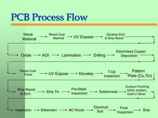
  • 1. PCB Process Flow Issue Material Resist Coat Material Oxide Develop Etch & Strip Resist DrillingLamination UV Expose UV Expose Electroless Copper Deposition Develop Pattern Plate (Cu,Tin) Surface Finishing HASL (solder), Gold or Silver SoldermaskStrip Tin Strip Resist & Etch NC RouteSilkscreen AOI T-Up Inspection Pre-Mask Inspection Inspection Electrical Test Final Inspection Resist Coat Panel Ship
  • 2. Tooling  Gerber files are panelized – Optimum panel utilization is key  Drill program is generated at the same time  Panelized artwork is plotted – Negative image: internal layers – Positive image: external layers  CAM design rule check – Spacing – Annular ring – Soldermask clearance  First article inspection Drilled panel representative of production panel – Mechanically inspected
  • 3. Dryfilm Resist Coating  Epoxy/Glass laminates are used – Material thickness: .0025” - .125” – Typical copper weights .5 oz - 2 oz  Incoming inspection – Thickness – Copper weight – Surface imperfections Epoxy/Glass Copper Clad
  • 4. Inner layer Imaging  Material is coated with dryfilm resist (A) – Dryfilm is photo-sensitive – Resists etching chemistry  Artwork image is transferred onto coated panels – Artwork is placed over panels as they go into exposure units – Clear area on film allows for polymerization – Emulsion area prevents polymerization – Non-polymerized dryfilm develops away Dryfilm Copper Epoxy/Glass Dryfilm Image Exposed Copper (A) (B)
  • 5. Inner Layer Etch  Imaged panels are etched  Etching chemistry attacks exposed copper  Dryfilm is stripped Etch Process After Etch
  • 6. Automated Optical Inspection  AOI units inspect etched inner layers – Program: gerber down load – Program: artwork learned  AOI works off reflected light – Oxidation produces psuedo defects – Defects are displayed on monitor and verified  Inner layers are oxide coated after AOI
  • 7. Lamination  Inspected inner layers panels are kitted  Panels are layed up between two stainless steel plates – Prepreg is used as the bonding agent – B-stage, semi-cured FR4  Heat and pressure are applied to laminate the panels Layer 1 Layer 3 Layer 2 Layer 4 Layer 1 Layer 3 Layer 2 Layer 4 From 6 - 10 multilayers Prepreg Copper Foil Separator Sheet: 12 mil thick aluminum, used to avoid panel sticking Steel plate
  • 8. Drilling  NC Drill machines are used - 4 - 6 spindels / machine - Auto tool change  Stack heights up to 3 panels high - Drill size - Board thickness - Pad-to-hole ratio  Electroless copper plating - Permanganate desmear - 80 micro-inches thick
  • 9. Outer Layer Imaging  Drilled / plated panels are dryfilm coated  Panels are UV exposed - Positive image  Panels are developed - Exposing circuitry and holes
  • 10. Electrolytic Plating  Exposed areas of panel are electrolytically plated. - Copper (.001 min avg) - Tin  Dryfilm is stripped exposing unwanted copper  Unwanted copper is etched away  Tin is stripped.
  • 11. Soldermask (LPI, liquid-photoimageable)  The entire panel is coated with LPI S/M - Automated DP1000 screeners – Tack dried after coating  LPI expose and develop – Same as with I.L & O.L imaging  Soldermask is used to define the component holes and pads  Thermal cure: 1 hour @ 150 C
  • 12. Surface Finishing  HASL, Solder – Soldermask defines areas which are to be coated with solder – Entire panel is immersed in a bath of molten solder – Hot air knives blow off the excess solder  Silver  ENIG, Electroless nickel immersion gold
  • 13. Fabrication  Panels are silk-screened prior to fabrication  Boards are de-panelized with NC route machines - 4 spindles - Stack heights up to 4 panels high v Thickness v Tolerances v Radius
  • 14. Electrical Test  Tested for opens & shorts  Bed of nails  Netlist from gerber – Netlist compared to CAD netlist – IPC-356 format