
Recommended
Recommended
More Related Content
What's hot
What's hot (20)
Viewers also liked
Viewers also liked (7)
Similar to HFSS ANTENNA FOR KU BAND WITH DEFECTED GROUND STRUCTURES
Similar to HFSS ANTENNA FOR KU BAND WITH DEFECTED GROUND STRUCTURES (20)
Recently uploaded
Recently uploaded (20)
HFSS ANTENNA FOR KU BAND WITH DEFECTED GROUND STRUCTURES
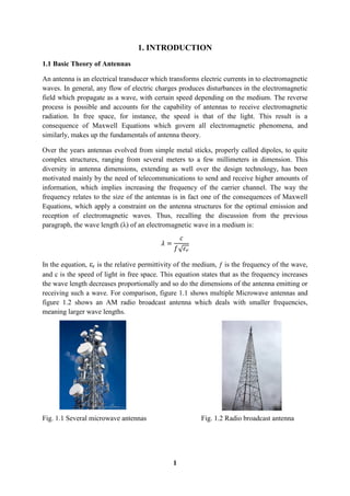
- 1. 1 1. INTRODUCTION 1.1 Basic Theory of Antennas An antenna is an electrical transducer which transforms electric currents in to electromagnetic waves. In general, any flow of electric charges produces disturbances in the electromagnetic field which propagate as a wave, with certain speed depending on the medium. The reverse process is possible and accounts for the capability of antennas to receive electromagnetic radiation. In free space, for instance, the speed is that of the light. This result is a consequence of Maxwell Equations which govern all electromagnetic phenomena, and similarly, makes up the fundamentals of antenna theory. Over the years antennas evolved from simple metal sticks, properly called dipoles, to quite complex structures, ranging from several meters to a few millimeters in dimension. This diversity in antenna dimensions, extending as well over the design technology, has been motivated mainly by the need of telecommunications to send and receive higher amounts of information, which implies increasing the frequency of the carrier channel. The way the frequency relates to the size of the antennas is in fact one of the consequences of Maxwell Equations, which apply a constraint on the antenna structures for the optimal emission and reception of electromagnetic waves. Thus, recalling the discussion from the previous paragraph, the wave length (λ) of an electromagnetic wave in a medium is: √ In the equation, εr is the relative permittivity of the medium, ƒ is the frequency of the wave, and c is the speed of light in free space. This equation states that as the frequency increases the wave length decreases proportionally and so do the dimensions of the antenna emitting or receiving such a wave. For comparison, figure 1.1 shows multiple Microwave antennas and figure 1.2 shows an AM radio broadcast antenna which deals with smaller frequencies, meaning larger wave lengths. Fig. 1.1 Several microwave antennas Fig. 1.2 Radio broadcast antenna
- 2. 2 1.2 Two Main Qualities of Antennas In general there are two main measures that define and qualify an antenna, the Resonant Capability and the Radiation Capability. The Resonant Capability is the most important characteristic of any antenna. It determines the specific frequency of electromagnetic waves (EM Wave) at which the antenna structure favors the establishment of the varying electric field lines which induce a potential difference between isolated parts of the antenna structure. This phenomenon occurs when the dimensions of the antenna structure allow half, full waves, or several periods of them. Then, the varying potential difference that those EM waves originate is emphasized from among the infinite number of frequencies traveling in the space. The Radiation Capability relates, in a single subject, two other important characteristics of an antenna. Readily, these two qualities are Antenna Efficiency (Antenna Gain) and Radiation Pattern. Together, Antenna Efficiency and Radiation Pattern talk about the way antennas use the energy supplied to radiate it all, in any or a particular direction, ideally, or most of it in the best real life scenarios. Radiation Capability, despite the short description given in this paragraph, involves a whole lot of branches of the Engineering, Physics, and Chemistry fields, for its analysis and development of improving technologies. As for instance, important research and experimentation is being performed in private and academic Microwave and Electromagnetic laboratories about the implementation of Double Negative Materials (DNG Materials), Meta materials indeed, for the gain improvement and size reduction of Microwave Antennas. Keeping the focus to this project, it is important to mention that the technology employed in the design of the multiband antenna, MSA, has lately become much popular with in this group of Microwave Antennas. 1.3 Remarkable Advantages and Disadvantages of Microstrip Antenna Technology MSA’s, as discussed earlier, are intrinsically light and small sized elements that can be fabricated with quite inexpensive materials, even in the retail market. Moreover, they are easily implemented with Microwave Integrated Circuits, as they are popularly built on Printed Circuit Boards (PCB’s). And, in favor of the project, they are capable of dual and triple frequency operation, as explained on the previous paragraphs. However, compared with most popular antenna structures for wireless applications, MSA’s suffer from two parameters which make them not the first option if high enough gain and wide band response is a requirement. Nevertheless, these disadvantages vary from geometry to geometry, which opens the possibility to employ computer aided simulations. Then, through a series of parametric analyzes, we may find the most convenient shape and dimensions, depending on the set goals and expectations for the project. This is in fact the approach followed in the design of the Multiband MSA.
- 3. 3 2. DESIGN OBJECTIVES Microstrip antennas are widely used due to their low profile, ease of fabrication, and capability of integration with other devices. Conventional Microstrip antenna has disadvantages of narrow bandwidth, low gain and cross-polarized radiation characteristics. Thus, enhancement of bandwidth and gain of Microstrip patch antenna (MPA) has become a challenging current research area. MPA with defected ground structure (DGS) has been reported for improving the performance of the patch antenna. The MPA with DGS has been reported for suppressing the cross-polarization level. Dual band with circular polarization in both planes has been achieved by using truncated DGS MPA. Rotated square-shape defect in the ground plane has been reported for enhancing the impedance bandwidth up to 50% with gain ranging from 3 dBi to 6 dBi. Several studies have been reported for DGS with Microstrip-line. DGS has been presented for reducing the size of low pass filter with wide- stop-band characteristics. Size reduction and harmonic suppression of Microstrip branch-line coupler by using DGS has been reported. A complimentary split ring resonator loaded ground plane for low-pass filter with compact size and wide stop band characteristics, and an equivalent circuit model has been presented. In present endeavor, a Microstrip linefed MPA with DGS is proposed for Ku-band applications. A circular shaped defect is integrated in the ground plane. A novel equivalent circuit model is presented for calculating the input impedance of the proposed MPA. The simple designing equations are presented and characteristics of the proposed antenna are analyzed by Finite Element Method (FEM) on Ansoft HFSS v.13. Fig. 2.1 Top and bottom view of proposed antenna
- 4. 4 3. SOFTWARE AIDED DESIGN The schematic of the proposed MPA is shown in Fig.3.1. A circular slot of radius a is integrated in the ground plane and an open ended Microstrip line of width wml and length Lml is placed on the opposite side of the ground plane. The radius of the circular slot is chosen, same as the radius of simple circular Microstrip patch antenna (CMPA). By making a circular defect of same radius in the ground plane, the new structure shows wide band characteristics. Fig. 3.1: Structure of the proposed antenna Table 3.1: Design specifications Parameter (mm) Parameter (mm) a 5.50 Lml 27.41 r1 1.50 h 1.6 wml 2.30 D 36
- 5. 5 The distance between the open-end-edge of Microstrip-line and centre of the circular slot is referred as feeding distance r1and it controls the return loss level of antenna. The design frequency for proposed structure is considered as 10 GHz. 3.1 Equivalent circuit model The modeling of equivalent circuit is divided in four parts; modeling of length l1and l2of Microstrip line, modeling of circular slot, modeling of fringing capacitance Cf due to discontinuity of Microstrip line, and modeling of coupling capacitance Cp between circular slot and Microstrip line. Circular Slot impedance is modeled by an ideal transformer with the Microstrip line, as shown in Fig. 3.1. Fig. 3.2: Equivalent circuit model of the proposed antenna 3.1.1 Modeling of Microstrip line A lossy Microstrip line is represented by a tank circuit of parameters, series resistant R, series inductance L, shunt conductance G, and shunt capacitance C. These parameters R, L, G and C are in per unit length and calculated for length l1and l2of Microstrip line.R1, L1, G1, C1and R2, L2, G2, C2are corresponding to the Microstrip line of length l1and l2 respectively. Losses in Microstrip line are due to imperfect conductor and dielectric, and is characterized by attenuation constant α, determined by α=αc +αd Where αc and αd are referred as conductor loss and dielectric loss respectively. 3.1.2 Modeling of circular slot The circular defect of diameter 2a is considered as a rectangular defect of length l and width w. The width of the rectangular defect is taken to be the same as the diameter of circular defect and length of the corresponding rectangular defect is calculated by equating the area. The input impedance offered by a rectangular slot can be calculated from the input impedance of a cylindrical dipole using Babinate’s principle.
- 6. 6 3.1.3 Modeling of fringing capacitance Due to the open-ended discontinuity, a fringing field of length l is developed at the end-edge of Microstrip line. A fringing capacitance Cf is used to model this fringing field and defined as √ 3.1.4 Modeling of coupling capacitance coupling between the two circuits is modeled by a coupling capacitance Cp and given by ( ) √( ) ( ) Where Cs is the slot capacitance, calculated from reactive part of the slot impedance given in Eq. (10), and the coupling coefficient Ck between two networks is determined by √ Where Q1is the quality factor of the Microstrip line and Q2is the quality factor of the slot. 3.1.5 Total Impedance The parallel slot impedance is given by Z’ slot=N. Zslot The parallel slot impedance Z’slot, impedance Zp offered by coupling capacitance Cp, and impedance Zf due to fringing capacitance Cf are added in parallel with impedance Z of Microstrip line. Where Z is the impedance offered by Microstrip line and determined by adding the impedances Z1and Z2in series. The equivalent circuit model of the proposed structure is shown in Fig. 3.2. Reflection coefficient, VSWR and Return loss is calculated as ( ) S11 =20 log (|r|)
- 7. 7 4. RESULTS The proposed structure is analyzed on Ansoft HFSS v.13.FR4_epoxy substrate of dimension 36 mm*36 mm*0.762 mm is used to fabricate the prototype. The dielectric constant εr, loss tangent, and thickness h of the substrate are as 2.2, 0.0009 and 1.6 mm respectively. Fig. 4.1: Patched Antenna designed on HFSS v13 Fig. 4.2: Patch Antenna Covered By Airbox The Microstrip-line-fed antenna with circular shape defect inthe ground plane is designed. Accurate design-ing equations are presented for wideband Microstrip antennafor the proposed structure. A novel equivalent circuit model ispresented for proposed prototype. An impedance bandwidth of56.67% ranging from 9.8 GHz to 17.55 GHz has been achieved. Thesimulated, measured and theoretical results are in good agree-ment. A gain of 5–12.08
- 8. 8 dBi is achieved in impedance bandwidth.The antenna produces good radiation pattern in the impedancebandwidth range. The Cross-Polarization levels are below −35 dBand −20 dB in H-Plane and E-Plane respectively. The isolations between the Co-Polar and Cross- Polarization levels are about 35 dBin H-Plane and 15 dB in E-Plane. Thus, designed antenna is a suitable candidate for Ku-band applications with good radiation characteristics. Fig. 4.3: Retain loss curve Fig. 4.4: Radiation pattern 10.00 11.00 12.00 13.00 14.00 15.00 16.00 Freq [GHz] -35.00 -30.00 -25.00 -20.00 -15.00 -10.00 -5.00 dB(St(feed_T1,feed_T1)) HFSSDesign1XY Plot 1 ANSOFT m 1 Curve Info dB(St(feed_T1,feed_T1)) Setup1 : Sw eep Name X Y m 1 12.5226 -31.9354 -23.00 -16.00 -9.00 -2.00 90 60 30 0 -30 -60 -90 -120 -150 -180 150 120 HFSSDesign1Radiation Pattern 5 ANSOFT Curve Info dB(rETotal) Setup1 : LastAdaptive Freq='12.52GHz' Phi='0deg' dB(rETotal) Setup1 : LastAdaptive Freq='12.52GHz' Phi='90deg'
- 9. 9 REFERENCES [1] M.K. Khandelwal et al./Int.J.Electron.Commun.(AEÜ)68(2014)951–957 http://dx.doi.org/10.1016/j.aeue.2014.04.017 [2] A Novel Neural Network for the Synthesis of Antennas and Microwave Devices Heriberto Jose Delgado, Member, IEEE, Michael H. Thursby, Senior Member, IEEE, and Fredric M. Ham, Senior Member, IEEE IEEE TRANSACTIONS ON NEURAL NETWORKS, VOL. 16, NO. 6, NOVEMBER 2005 [3] Design of a Widebland Microstrip Antenna and the Use of Artificial Neural Networks in Parameter Calculation Dipak K. Neog1, Shyam S. PattnaiK, Dhruba. C. Panda2, Swapna Devr, Bonomali Khuntia3, and Malaya Dutta4 IEEE Antennas and Propagation Magazine, Vol. 47, No.3, June 2005