SlideShare a Scribd company logo
1 of 61
Download to read offline
SOLAR CELL GCT DEE
SESSION 2014-2018 Page 1
Chapter 1
INTRODUCTION
1.1 About The Solar Cell
A solar cell (photovoltaic cell or photoelectric cell) is a solid state electrical device that
converts the energy of light directly into electricity by the photovoltaic effect. The energy of
light is transmitted by photons-small packets or quantum of light. Electrical energy is stored in
electromagnetic fields, which in turn can make a current of electrons flow. Assemblies of solar
cells are used to make solar modules which are used to capture energy from sunlight. When
multiple modules are assembled together (such as prior to installation on a pole-mounted
tracker system), the resulting integrated group of modules all oriented in one plane is referred
as a solar panel. The electrical energy generated from solar modules, is an example of solar
energy. Photovoltaic is the field of technology and research related to the practical application
of photovoltaic cells in producing electricity from light, though it is often used specifically to
refer to the generation of electricity from sunlight. Cells are described as photovoltaic cells
when the light source is not necessarily sunlight. These are used for detecting light or other
electromagnetic radiation near the visible range, for example Infrared detectors, or
measurement of light intensity.
Fig 1.1 :- Solar Cell
SOLAR CELL GCT DEE
SESSION 2014-2018 Page 2
A solar cell, or photovoltaic cell, is an electrical device that converts the energy of light directly
into electricity by the photovoltaic effect, which is a physical and chemical phenomenon. It is a
form of photoelectric cell, defined as a device whose electrical characteristics, such
as current, voltage, or resistance, vary when exposed to light. Individual solar cell devices can
be combined to form modules, otherwise known as solar panels. In basic terms a single
junction silicon solar cell can produce a maximum open-circuit voltage of approximately 0.5 to
0.6 volts. Solar cells are described as being photovoltaic, irrespective of whether the source
is sunlight or an artificial light. They are used as a photo detector (for example infrared
detectors), detecting light or other electromagnetic radiation near the visible range, or
measuring light intensity.
The operation of a photovoltaic (PV) cell requires three basic attributes:
 The absorption of light, generating either electron-hole pairs or excisions.
 The separation of charge carriers of opposite types.
 The separate extraction of those carriers to an external circuit.
In contrast, a solar thermal collector supplies heat by absorbing sunlight, for the purpose of
either direct heating or indirect electrical power generation from heat. A "photo electrolytic
cell" (photo-electro-chemical cell), on the other hand, refers either to a type of photovoltaic cell
(like that developed by Edmond Becquerel and modern dye-sensitized solar cells), or to a
device that splits water directly into hydrogen and oxygen using only solar illumination.
1.2 Introduction of Energy
1.2.1 Non-Renewable Energy
Non-Renewable energy is energy which is taken from the sources that are available on the earth
in limited quantity and will vanish fifty-sixty years from now. Non-renewable sources are not
environmental friendly and can have serious affect on our health. They are called non-
renewable because they cannot be re-generated within a short span of time. Non-renewable
sources exist in the form of fossil fuels, natural gas, oil and coal.
According to recent predictions, the inevitable permanent de-cline in the global oil production
rate is expected to start within the next 10-20 years. However, the combustion of fossil fuels in
the past has already harmful effects on the delicate balance of nature on our planet. Today,
about 20 X 1012 kg of carbon dioxide are put into the atmosphere every year, mainly by
burning fossil fuel. Today’s plants are unable to absorb this huge amount of extra CO2.
SOLAR CELL GCT DEE
SESSION 2014-2018 Page 3
1.2.2 Renewable Energy
Renewable energy is energy which is generated from natural sources i.e. sun, wind, rain, tides
and can be generated again and again as and when required. They are available in plenty and by
far most the cleanest sources of energy available on this planet. For e.g.: Energy that we receive
from the sun can be used to generate electricity. Similarly, energy from wind, geothermal,
biomass from plants, tides can be used this form of energy to another form.
Worldwide, oil prices will then rise considerably favouring the introduction of various
renewable energy sources such as the direct conversion of solar energy (solar cells), but also
others like for example, hydroelectric- and wind-power systems. Renewable energy sources
neither run out nor have any significant harmful effects on our environment.
Renewable energy is energy that is collected from renewable resources, which are naturally
replenished on a human timescale, such as sunlight, wind, rain, tides, waves, and geothermal
heat. Renewable energy often provides energy in four important areas: electricity
generation, air and water heating & cooling, transportation, and rural (off-grid) energy services.
Renewable energy resources exist over wide geographical areas, in contrast to other energy
sources, which are concentrated in a limited number of countries.
Rapid deployment of renewable energy and energy efficiency is resulting in significant energy
security, climate change mitigation, and economic benefits. The results of a recent review of
the literature concluded that as greenhouse gas (GHG) emitters begin to be held liable for
damages resulting from GHG emissions resulting in climate change, a high value for liability
mitigation would provide powerful incentives for deployment of renewable energy
technologies.
In international public opinion surveys there is strong support for promoting renewable sources
such as solar power and wind power. At the national level, at least 30 nations around the world
already have renewable energy contributing more than 20 percent of energy supply. National
renewable energy markets are projected to continue to grow strongly in the coming decade and
beyond.
SOLAR CELL GCT DEE
SESSION 2014-2018 Page 4
1.3 Solar Energy
Solar energy, radiant light and heat from the sun, is harnessed using a range of ever-evolving
technologies such as solar heating, concentrated solar power (CSP), concentrator
photovoltaic (CPV), solar architecture and artificial photosynthesis. Solar technologies are
broadly characterized as either passive solar or active solar depending on the way they capture,
convert and distribute solar energy.
Passive solar techniques include orienting a building to the Sun, selecting materials with
favourable thermal mass or light dispersing properties, and designing spaces that naturally
circulate air. Active solar technologies encompass solar thermal energy, using solar
collectors for heating, and solar power, converting sunlight into electricity either directly
using photovoltaic (PV), or indirectly using concentrated solar power (CSP).
A photovoltaic system converts light into electrical direct current (DC) by taking advantage of
the photoelectric effect. Solar PV has turned into a multi-billion, fast-growing industry,
continues to improve its cost-effectiveness, and has the most potential of any renewable
technologies together with CSP. Concentrated solar power (CSP) systems use lenses or mirrors
and tracking systems to focus a large area of sunlight into a small beam. Commercial
concentrated solar power plants were first developed in the 1980s. CSP-Stirling has by far the
highest efficiency among all solar energy technologies.
In 2011, the International Energy Agency said that "the development of affordable,
inexhaustible and clean solar energy technologies will have huge longer-term benefits. It will
increase countries' energy security through reliance on an indigenous, inexhaustible and mostly
import-independent resource, enhance sustainability, reduce pollution, lower the costs of
mitigating climate change, and keep fossil fuel prices lower than otherwise. These advantages
are global. Hence the additional costs of the incentives for early deployment should be
considered learning investments; they must be wisely spent and need to be widely
shared".[48]
Italy has the largest proportion of solar electricity in the world, in 2015 solar
supplied 7.8% of electricity demand in Italy. In 2016, after another year of rapid growth, solar
generated 1.3% of global power.
SOLAR CELL GCT DEE
SESSION 2014-2018 Page 5
1.4 History and Development of Solar Cell Technology
The development of solar cell technology began with the 1839 research of French physicist
Antoine-César Becquerel. Becquerel observed the photovoltaic effect while experimenting with
a solid electrode in an electrolyte solution when he saw a voltage develop when light fell upon
the electrode. The major events are discussed briefly below, and other milestones can be
accessed by clicking on the image shown below.
Charles Fritts - First Solar Cell: The first genuine solar cell was built around 1883 by Charles
Fritts, who used junctions formed by coating selenium (a semiconductor) with an extremely
thin layer of gold. The device was only about 1 percent efficient.
Albert Einstein - Photoelectric Effect: Albert Einstein explained the photoelectric effect in 1905
for which he received the Nobel Prize in Physics in 1921.
Russell Ohl - Silicon Solar Cell: Early solar cells, however, had energy conversion efficiencies
of under one percent. In 1941, the silicon solar cell was invented by Russell Ohl.
Gerald Pearson, Calvin Fuller and Daryl Chapin - Efficient Solar Cells: In 1954, three
American researchers, Gerald Pearson, Calvin Fuller and Daryl Chapin, designed a silicon solar
cell capable of a six percent energy conversion efficiency with direct sunlight. They created the
first solar panels.
The photovoltaic effect was experimentally demonstrated first by French physicist Edmond
Becquerel. In 1839, at age 19, he built the world's first photovoltaic cell in his father's
laboratory. Willoughby Smith first described the "Effect of Light on Selenium during the
passage of an Electric Current" in a 20 February 1873 issue of Nature. In 1883 Charles
Fritts built the first solid state photovoltaic cell by coating the semiconductor selenium with a
thin layer of gold to form the junctions; the device was only around 1% efficient.
In 1888 Russian physicist Aleksandr Stoletov built the first cell based on the outer photoelectric
effect discovered by Heinrich Hertz in 1887.
In 1905 Albert Einstein proposed a new quantum theory of light and explained
the photoelectric effect in a landmark paper, for which he received the Nobel Prize in
Physics in 1921.
Russell Ohl patented the modern junction semiconductor solar cell in 1946[8]
while working on
the series of advances that would lead to the transistor.
SOLAR CELL GCT DEE
SESSION 2014-2018 Page 6
Chapter 2
PRINCIPLE OF SOLAR CELL
2.1 About Solar Cell
Solar cells are devices which convert solar energy directly into electricity, either directly via
the photovoltaic effect, or indirectly by first converting the solar energy to heat or chemical
energy. Assemblies of cells used to make solar modules which are used to capture energy from
sunlight, are known as solar panels. The energy generated from these solar modules, referred to
as solar power. Cells are described as photovoltaic cells when the light source is not necessarily
sunlight (lamplight, artificial light etc). The amount of power available from a PV device is
determined by -the type and area of the material, the intensity of the sun light , the wavelength
of the sunlight.
2.1.1 Theory
The solar cell work in several steps
 Photons in sunlight hit the solar panel and are absorbed by semiconducting material
such as silicon.
 An array of solar cells converts solar energy into a usable amount of direct current (DC)
electricity.
Fig 2.1 :- Working mechanism of solar cell
SOLAR CELL GCT DEE
SESSION 2014-2018 Page 7
 Electrons are excited from their current molecular/atomic orbital. Once excited an electron
can either dissipate the energy as heat and return to its orbital or travel through the cell
until it reaches an electrode. Current flows through the material to cancel the potential and
this electricity is captured. The chemical bonds of the material are vital for this process to
work, and usually silicon is used in two layers, one layer being doped with boron, the
other phosphorus. These layers have different chemical electric charges and subsequently
both drive and direct the current of electrons.
 An inverter can convert the power to alternating current (AC). The most commonly known
solar cell is configured as a large-area p–n junction made from silicon. Other possible solar
cell types are organic solar cells, dye sensitized solar cells, perovskite solar cells, quantum
dot solar cells etc. The illuminated side of a solar cell generally have a transparent
conducting film for allowing light to enter into active material and to collect the generated
charge carriers. Typically, films with high transmittance and high electrical conductance
such as indium tin oxide, conducting polymers or conducting nanowire networks are used
for the purpose.
2.2 Solar Cell
There are several types of solar cells. However, more than 90 % of the solar cells currently
made worldwide consist of wafer-based silicon cells. They are either cut from a single crystal
rod or from a block composed of many crystals and are correspondingly called mono-
crystalline or multi-crystalline silicon solar cells. Wafer-based silicon solar cells are
approximately 200 μm thick. Another important family of solar cells is based on thin-films,
which are approximately 1-2 μm thick and therefore require significantly less active,
semiconducting material.
Thin-film solar cells can be manufactured at lower cost in large production quantities; hence
their market share will likely increase in the future. However, they indicate lower efficiencies
than wafer-based silicon solar cells, which means that more exposure surface and material for
the installation is required for a similar performance. A number of solar cells electrically
connected to each other and mounted in a single support structure or frame is called a
‘photovoltaic module’. Modules are designed to supply electricity at a certain voltage, such as a
common 12 volt system. The current produced is directly dependent on the intensity of light
reaching the module. Several modules can be wired together to form an array. Photovoltaic
modules and arrays produce direct-current electricity.
SOLAR CELL GCT DEE
SESSION 2014-2018 Page 8
2.3 Types of Solar Cell
Based on the material used different types of solar cell are
Fig 2.2 :- Types of Solar cell
Materials presently used for photovoltaic solar cells include monocrystalline silicon,
polycrystalline silicon, amorphous silicon, cadmium telluride, and copper indium gallium
selenide. Many currently available solar cells are made from bulk materials that are cut into
wafers between 180 to 240 micrometers thick that are then processed like other
semiconductors. Other materials are made as thin-films layers, organic dyes, and organic
polymers that are deposited on supporting substrates. A third group are made from nanocrystals
and used as quantum dots (electron-confined nanoparticles). Silicon remains the only material
that is well-researched in both bulk and thin-film forms.
In international public opinion surveys there is strong support for promoting renewable sources
such as solar power and wind power. When multiple modules are assembled together (such as
prior to installation on a pole-mounted tracker system), the resulting integrated group of
modules all oriented in one plane is referred as a solar panel. The electrical energy generated
from solar modules, is an example of solar energy. At the national level, at least 30 nations
around the world already have renewable energy contributing more than 20 percent of energy
supply.
SOLAR CELL GCT DEE
SESSION 2014-2018 Page 9
Some Other Types of Solar Cell
A solar cell (also called photovoltaic cell or photoelectric cell) is a solid state electrical device
that converts the energy of light directly into electricity by the photovoltaic effect. The
following are the different types of solar cells
 Amorphous Silicon solar cell (a-Si)
 Biohybrid solar cell
 Cadmium telluride solar cell (CdTe)
 Concentrated PV cell (CVP and HCVP)
 Copper indium gallium selenide solar cells (CI(G)S)
 Crystalline silicon solar cell (c-Si)
 Dye-sensitized solar cell (DSSC)
 Gallium arsenide germanium solar cell (GaAs)
 Hybrid solar cell
 Luminescent solar concentrator cell (LSC)
 Micromorph (tandem-cell using a-Si/μc-Si)
 Monocrystalline solar cell (mono-Si)
 Multi-junction solar cell (MJ)
 Nanocrystal solar cell
 Organic solar cell (OPV)
 Perovskite solar cell
 Photoelectrochemical cell (PEC)
 Plasmonic solar cell
 Polycrystalline solar cell (multi-Si)
 Quantum dot solar cell
 Solid-state solar cell
 Thin-film solar cell (TFSC)
 Wafer solar cell, or wafer-based solar cell crystalline.
SOLAR CELL GCT DEE
SESSION 2014-2018 Page 10
2.4 Solar Cell Working
The solar cell works in following steps:
1. Photons in sunlight hit the solar panel and are absorbed by semiconducting materials,
such as silicon. Photons with energy equal to the band gap energy are absorbed to create
free electrons. Photons with less energy than the band gap energy pass through the
material.
2. Formation of electron-hole pair (exciton).
3. Exciton diffusion to Junction.
4. Charge separation- Electrons (negatively charged) are knocked loose from their atoms,
causing an electric potential difference. Current starts flowing through the material to
cancel the potential and this electricity is captured i.e. Electrons that are created on the
n-type side may travel through the wire, power the load, and continue through the wire
until they reach the p-type semiconductor-metal contact. Here, they recombine with a
hole that was either created as an electron-hole pair on the p-type side of the solar cell.
Due to the special composition of solar cells, the electrons are only allowed to move in
a single direction.
5. An array of solar cells converts solar energy into a usable amount of direct current (DC)
electricity.
2.4.1 Equivalent Circuit of a Solar Cell
Fig 2.3 :- Circuit diagram of Solar cell
Fig 2.4:- Symbol of Solar Cell
SOLAR CELL GCT DEE
SESSION 2014-2018 Page 11
To understand the electronic behavior of a solar cell, it is useful to create a model which is
electrically equivalent, and is based on discrete ideal electrical components whose behavior is
well defined. An ideal solar cell may be modelled by a current source in parallel with a diode;
in practice no solar cell is ideal, so a shunt resistance and a series resistance component are
added to the model. The resulting equivalent circuit of a solar cell is shown on the left. Also
shown, on the right, is the schematic representation of a solar cell for use in circuit diagrams.
2.4.2 Characteristic Equation
From the equivalent circuit it is evident that the current produced by the solar cell is equal to
that produced by the current source, minus that which flows through the diode, minus that
which flows through the shunt resistor.
where
 I = output current (ampere)
 IL = photogenerated current (ampere)
 ID = diode current (ampere)
 ISH = shunt current (ampere).
The current through these elements is governed by the voltage across them:
where
 Vj = voltage across both diode and resistor RSH (volt)
 V = voltage across the output terminals (volt)
 I = output current (ampere)
 RS = series resistance (Ω).
By the Shockley diode equation, the current diverted through the diode is:
where
 I0 = reverse saturation current (ampere)
 n = diode ideality factor (1 for an ideal diode)
 q = elementary charge
 k = Boltzmann's constant
An alternative derivation produces an equation similar in appearance, but with V on the left-
hand side. The two alternatives are identities; that is, they yield precisely the same results.
Since the parameters I0, n, RS, and RSH cannot be measured directly.
SOLAR CELL GCT DEE
SESSION 2014-2018 Page 12
2.5 Efficiency
Electrical efficiency (also called conversion efficiency) is a contributing factor in the selection
of a photovoltaic system. However, the most efficient solar panels are typically the most
expensive, and may not be commercially available. Therefore, selection is also driven by cost
efficiency and other factors.
The electrical efficiency of a PV cell is a physical property which represents how much
electrical power a cell can produce for a given insolation. The basic expression for maximum
efficiency of a photovoltaic cell is given by the ratio of output power to the incident solar
power (radiation flux times area).
The efficiency is measured under ideal laboratory conditions and represents the maximum
achievable efficiency of the PV material. Actual efficiency is influenced by the output Voltage,
current, junction temperature, light intensity and spectrum.
The most efficient type of solar cell to date is a multi-junction concentrator solar cell with an
efficiency of 46.0% produced by Fraunhofer ISE in December 2014. The highest efficiencies
achieved without concentration include a material by Sharp Corporation at 35.8% using a
proprietary triple-junction manufacturing technology in 2009, and Boeing Spectrolab (40.7%
also using a triple-layer design). The US company SunPower produces cells that have an
efficiency of 21.5%, well above the market average of 12–18%.
There is an ongoing effort to increase the conversion efficiency of PV cells and modules,
primarily for competitive advantage. In order to increase the efficiency of solar cells, it is
important to choose a semiconductor material with an appropriate band gap that matches the
solar spectrum. This will enhance the electrical and optical properties. Improving the method of
charge collection is also useful for increasing the efficiency. There are several groups of
materials that are being developed. Ultrahigh-efficiency devices (η>30%) are made by using
GaAs and GaInP2 semiconductors with multi junction tandem cells. High-quality, single-
crystal silicon materials are used to achieve high-efficiency, low cost cells (η>20%).
SOLAR CELL GCT DEE
SESSION 2014-2018 Page 13
Chapter 3
MANUFACTURING OF SOLAR CELL
3.1 Manufacturing Technology and process of Solar Cell
3.1.1 Purification of Silicon
Fig 3.1 :- Purification of Silicon
The basic component of a solar cell is intrinsic silicon, which is not pure in its natural state. To
make solar cells, the raw materials—silicon dioxide of either quartzite gravel or crushed
quartz—are first placed into an electric arc furnace, where a carbon arc is applied to release the
oxygen. A Graphite and Thermal insulator trap the heat and maintain the furnace at required
temperature for gangue (impurity) to form a slag. The products are carbon dioxide and molten
silicon. Silicon ingot is pulled down from the molten silicon using seed silicon crystallization
and floating zone technique. Passing impure silicon in same direction several times that
separates impurities- and impure end is later removed.
This process yields silicon with one percent impurity, useful in many industries but not the
solar cell industry. At this point, the silicon is still not pure enough to be used for solor cells
and requires further purification. Pure silicon is derived from such silicon dioxides as quartzite
gravel (the purest silica) or crushed quartz.
SOLAR CELL GCT DEE
SESSION 2014-2018 Page 14
3.1.2 Ingot and Wafer Preparation
Fig 2.4 :- System of Ingot and Wafer Preparation
Solar cells are made from silicon boules, polycrystalline structures that have the atomic
structure of a single crystal. The most commonly used process for creating the boule is called
the Czochralski method. In this process, a seed crystal of silicon is dipped into melted
polycrystalline silicon.
As the seed crystal is withdrawn and rotated, a cylindrical ingot or "boule" of silicon is formed.
The ingot withdrawn is unusually pure, because impurities tend to remain in the liquid. From
the boule, silicon wafers are sliced one at a time using a circular saw whose inner diameter cuts
into the rod, or many at once with a multi wire saw. (A diamond saw produces cuts that are as
wide as the wafer—. 5 millimeter thick.). Only about one-half of the silicon is lost from the
boule to the finished circular wafer—more if the wafer is then cut to be rectangular or
hexagonal. Only about one-half of the silicon is lost from the boule to the finished circular
wafer—more if the wafer is then cut to be rectangular or hexagonal. Rectangular or hexagonal
wafers are sometimes used in solar cells because they can be fitted together perfectly, thereby
utilizing all available space on the front surface of the solar cell. The wafers are then polished
to remove saw marks.
SOLAR CELL GCT DEE
SESSION 2014-2018 Page 15
3.1.3 Doping
The traditional way of doping silicon wafers with boron and phosphorous is to introduce a
small amount of boron during the Czochralski process. The wafers are then sealed back to back
and placed in a furnace to be heated to slightly below the melting point of silicon (2,570
degrees Fahrenheit or 1,410 degrees Celsius) in the presence of phosphorous gas. The
phosphorous atoms "burrow" into the silicon, which is more porous because it is close to
becoming a liquid.
The temperature and time given to the process is carefully controlled to ensure a uniform
junction of proper depth. These diffusion processes are usually performed through the use of a
batch tube furnace or an in-line continuous furnace. The basic furnace construction and process
are very similar to the process steps used by packaging engineers.
3.1.4 Screen Printing
Fig 2.5 :- View of Screen Printing of Solar Cell
Electrical contacts are formed through squeezing a metal paste through mesh screens to create a
metal grid. This metal paste (usually Ag or Al) needs to be dried so that subsequent layers can
be screen-printed using the same method. It is predicted that second generation cells will
dominate the residential solar market. This electric field acts as a diode, allowing (and even
pushing) electrons to flow from the P side to the N side. As a last step, the wafer is heated in a
continuous firing furnace at temperatures ranging from 780 to 900°C. These grid- pattern metal
screens act as collector electrodes that carry electrons and complete the electrical continuity in
the circuit.
SOLAR CELL GCT DEE
SESSION 2014-2018 Page 16
2.3.5 Stringing And Tabbing
Fig 2.6 :- View of Stringing and Tabbing
Electrical contacts connect each solar cell to another and to the receiver of produced current.
The contacts must be very thin (at least in the front) so as not to block sunlight to the cell
electrical use. There are also many rebates available to help you save 40-60% on the cost of
acquiring your system. This causes further disruption of electrical neutrality.
if an external current path is provided, electrons will flow through the path to the P side to unite
with holes that the electric field sent there, doing work for us along the way. The outer shell,
however, is only half full with just four electrons (Valence electrons). The electron flow
provides the current, and the cell's electric field causes a voltage. Instead of having free
electrons, P-type ("p" for positive) has free openings and carries.
the heat and maintain the furnace at required temperature for gangue (impurity) to form a slag.
The products are carbon dioxide and molten silicon. Silicon ingot is pulled down from the
molten silicon using seed silicon crystallization and floating zone technique. For more
information on rebates and incentives for installing a solar power system on your home or
business look up "Energy Incentives" on the IRS website or check with your local tax adviser
for details.
Metals such as palladium/silver, nickel, or copper are vacuum-evaporated After the contacts are
in place, thin strips ("fingers") are placed between cells. The most commonly used strips are
tin-coated copper.
SOLAR CELL GCT DEE
SESSION 2014-2018 Page 17
3.1.6 Antireflective Coating
Because pure silicon is shiny, it can reflect up to 35 percent of the sunlight. To reduce the
amount of sunlight lost, an anti-reflective coating is put on the silicon wafer- mostly titanium
dioxide, silicon oxide and some others are used. The material used for coating is either heated
until its molecules boil off and travel to the silicon and condense, or the material undergoes
sputtering. In this process, a high voltage knocks molecules off the material and deposits them
onto the silicon at the opposite electrode.
Yet another method is to allow the silicon itself to react with oxygen- or nitrogen-containing
gases to form silicon dioxide or silicon nitride. Commercial solar cell manufacturers use silicon
nitride. Another method to make silicon absorb more light is to make its top surface grained,
i.e. pyramid shaped nanostructures that yield 70% absorption that reaches the cell surface after
passing through anti-reflective coating.
Fig 2.7 :- Antireflective Coating on Solar Cell
3.1.7 Module Manufacturing
The finished solar cells are then encapsulated; that is, sealed into silicon rubber or ethylene
vinyl acetate. Solar module assembly usually involves soldering cells together to produce a 36-
cell string (or longer) and laminating it between toughened glass on the top and a polymeric
backing sheet on the bottom. The encapsulated solar cells are then placed into an aluminum
frame that has a Mylar or tedlar back sheet and a glass or plastic cover. Frames are usually
applied to allow for mounting in the field, or the laminates may be separately integrated into a
mounting system for a specific application such as integration into a building.
SOLAR CELL GCT DEE
SESSION 2014-2018 Page 18
Chapter 4
MATERIAL USE IN SOLAR CELL
4.1 Materials Used in Solar Cell
Various materials display varying efficiencies and have varying costs. Materials for efficient
solar cells must have characteristics matched to the spectrum of available light. Some cells are
designed to efficiently convert wavelengths of solar light that reach the Earth surface.
However, some solar cells are optimized for light absorption beyond Earth's atmosphere as
well.
Light absorbing materials can often be used in multiple physical configurations to take
advantage of different light absorption and charge separation mechanisms. Materials presently
used for photovoltaic solar cells include monocrystalline silicon, polycrystalline silicon,
amorphous silicon, cadmium telluride, and copper indium selenide/sulfide. Many currently
available solar cells are made from bulk materials that are cut into wafers between 180 to 240
micrometers thick that are then processed like other semiconductors.
4.1.1 Crystalline Silicon
By far, the most prevalent bulk material for solar cells is crystalline silicon (abbreviated as a
group as c-Si), also known as "solar grade silicon". Bulk silicon is separated into multiple
categories according to crystallinity and crystal size in the resulting ingot, ribbon, or wafer.
Fig 4.1 :- Crystalline silicon
SOLAR CELL GCT DEE
SESSION 2014-2018 Page 19
a.) Monocrystalline Silicon (C-Si): often made using the Czochralski process.
Singlecrystal wafer cells tend to be expensive, and because they are cut from cylindrical
ingots, do not completely cover a square solar cell module without a substantial waste of
refined silicon. Hence most c-Si panels have uncovered gaps at the four corners of the
cells.
b.) Polycrystalline Silicon & Multicrystalline Silicon, (Poly-Si Or Mc-Si):
made from cast square ingots — large blocks of molten silicon carefully cooled and
solidified. Poly- Si cells are less expensive to produce than single crystal silicon cells, but
are less efficient. United States Department of Energy data show that there were a higher
number of polycrystalline sales than monocrystalline silicon sales.
c.) Ribbon Silicon: It is a type of polycrystalline silicon. it is formed by drawing flat thin
films frommolten silicon and results in a polycrystalline structure. These cells have lower
efficiencies than poly-Si, but save on production costs due to a great reduction in silicon
waste, as this approach does not require sawing from ingots.
d.) Mono Si & Multi Silicon: Developed in the 2000s and introduced commercially
around 2009, mono-like-multi, or cast-mono, uses existing polycrystalline casting
chambers with small "seeds" of mono material. The result is a bulk mono-like material
with poly around the outsides. When sawn apart for processing, the inner sections are
high-efficiency mono-like cells (but square instead of "clipped"), while the outer edges
are sold off as conventional poly. The result is line that produces mono-like cells at poly-
like prices.
4.1.2 Thin films
Thin-film technologies reduce the amount of material required in creating the active material of
solar cell. Most thin film solar cells are sandwiched between two panes of glass to make a
module. Since silicon solar panels only use one pane of glass, thin film panels are
approximately twice as heavy as (A-Si) are three thin-film technologies often used as outdoor
photovoltaic solar power production. CdTe technology is most cost competitive among them.
Silicon thin-film cells are mainly deposited by chemical vapor deposition (typically plasma-
enhanced, PE-CVD) from silane gas and hydrogen gas. Depending on the deposition
parameters, this can yield amorphous silicon (a-Si or a-Si:H), protocrystalline silicon
or nanocrystalline silicon (nc-Si or nc-Si:H), also called microcrystalline silicon. Amorphous
silicon is the most well-developed thin film technology to-date. An amorphous silicon (a-Si)
solar cell is made of non-crystalline or microcrystalline silicon.
SOLAR CELL GCT DEE
SESSION 2014-2018 Page 20
4.1.3 Cadmium Telluride Solar Cell
A cadmium telluride solar cell uses a cadmium telluride (CdTe) thin film, a semiconductor
layer to absorb and convert sunlight into electricity. Solarbuzz has reported that the lowest
quoted thin-film module price stands at US$0.84 per watt-peak, with the lowest crystalline
silicon (c-Si) module at $1.06 per watt-peak.
4.1.4 Copper Indium Gallium Selenide
Copper indium gallium selenide (CIGS) is a direct band gap material. It has the highest
efficiency (~20%) among thin film materials (see CIGS solar cell). Traditional methods of
fabrication involve vacuum processes including co-evaporation and sputtering. Recent
developments at IBM and Nanosolar attempt to lower the cost by using non-vacuum solution
processes.
Amorphous silicon has a higher bandgap (1.7 eV) than crystalline silicon (c-Si) (1.1 eV), which
means it absorbs the visible part of the solar spectrum more strongly than the higher power
density infrared portion of the spectrum. The production of a-Si thin film solar cells uses glass
as a substrate and deposits a very thin layer of silicon by plasma-enhanced chemical vapor
deposition (PECVD).
4.1.5 Gallium Arsenide Multijunction
High-efficiency multijunction cells were originally developed for special applications such as
satellites and space exploration, but at present, their use in terrestrial concentrators might be the
lowest cost alternative in terms of $/kWh and $/W. These multijunction cells consist of
multiple thin films produced using metalorganic vapour phase epitaxy. A triple-junction cell,
for example, may consist of the absorb electromagnetic radiation over a portion of the
spectrum. Combinations of semiconductors are carefully chosen to absorb nearly all of the solar
spectrum, thus generating electricity from as much of the solar energy as possible.
GaAs based multijunction devices are the most efficient solar cells to date. In 15 October 2012,
triple junction metamorphic cell reached a record high of 44%. Tandem solar cells based on
monolithic, series connected, gallium indium phosphide (GaInP), gallium arsenide GaAs, and
germanium Ge p–n junctions, are seeing demand rapidly rise. Between December 2006 and
December 2007, the cost of 4N gallium metal rose from about $350 per kg to $680 per kg.
Additionally, germanium metal prices have rise substantially to $1000–1200 per kg this year.
SOLAR CELL GCT DEE
SESSION 2014-2018 Page 21
4.1.6 Light-Absorbing Dyes (DSSC)
Dye-sensitized solar cells (DSSCs) are made of low-cost materials and do not need elaborate
equipment to manufacture, so they can be made in a DIY fashion, possibly allowing players to
produce more of this type of solar cell than others. In bulk it should be significantly less
expensive than older solid-state cell designs. DSSC's can be engineered into flexible sheets, and
although its conversion efficiency is less than the best thin film cells, its price to compete with
fossil fuel electrical generation.
Typically a ruthenium metal organic dye (Ru-centered) is used as a monolayer of light
absorbing material. The dye-sensitized solar cell depends on a mesoporous layer of an titanium
dioxide to greatly amplify the surface area (200–300 m2/g TiO2, as compared to approximately
10 m2/g of flat single crystal).
4.1.7 Quantum Dot Solar Cells (QDSCs)
Quantum dot solar cells (QDSCs) are based on the Gratzel cell, or dye-sensitized solar cell,
architecture but employ low band gap semiconductor nanoparticles, fabricated with such small
crystallite sizes that they form quantum dots (such as CdS, CdSe, Sb2S3, PbS, etc.), instead of
organic or organometallic dyes as light absorbers. Quantum dots (QDs) have attracted much
interest because of their unique properties. Their size quantization allows for the band gap to be
tuned by simply changing particle size. They also have high extinction coefficients, and have
shown the possibility of multiple exciton generation.
4.1.8 Organic/Polymer Solar Cells
Organic solar cells are a relatively novel technology, yet hold the promise of a substantial price
reduction (over thin-film silicon) and a faster return on investment. These cells can be
processed from solution, hence the possibility of a simple roll-to-roll printing process, leading
to inexpensive, large scale production. Organic solar cells and polymer solar cells are built
from thin films (typically 100 nm) of organic semiconductors including polymers, such as poly
phenyl and small molecule compounds like copper phthalocyanine PCBM. Energy conversion
efficiencies achieved to date using conductive polymers are low compared to inorganic
materials. Protocrystalline silicon with a low volume fraction of nanocrystalline silicon is
optimal for high open circuit voltage.[60]
Nc-Si has about the same bandgap as c-Si and nc-Si
and a-Si can advantageously be combined in thin layers, creating a layered cell called a tandem
cell. The top cell in a-Si absorbs the visible light and leaves the infrared part of the spectrum
for the bottom cell in nc-Si.
SOLAR CELL GCT DEE
SESSION 2014-2018 Page 22
4.1.9 Silicon Thin Films
Silicon thin-film cells are mainly deposited by chemical vapor deposition (typically
plasmaenhanced, PE-CVD) from silane gas and hydrogen gas. Depending on the deposition
parameters, this can yield:
1. Amorphous Silicon (A-Si Or A-Si:H)
2. Protocrystalline Silicon
3. Nanocrystalline Silicon (Nc-Si Or Nc-Si:H) & Microcrystalline Silicon.
An amorphous silicon (a-Si) solar cell is made of amorphous or microcrystalline silicon and its
basic electronic structure is the p-i-n junction. a-Si is attractive as a solar cell material because
it is abundant and non-toxic (unlike its CdTe counterpart) and requires a low processing
temperature, enabling production of devices to occur on flexible and low-cost substrates. As the
amorphous structure has a higher absorption rate of light than crystalline cells, the complete
light spectrum can be absorbed with a very thin layer of photo-electrically active material. A
film only 1 micron thick can absorb 90% of the usable solar energy.
This reduced material requirement along with current technologies being capable of large-area
deposition of a-Si, the scalability of this type of cell is high. Recently, solutions to overcome
the limitations of thin-film crystalline silicon have been developedAnti-reflective coatings can
also be applied to create destructive interference within the cell. This can be done by
modulating the Refractive index of the surface coating; if destructive interference is achieved,
there will be no reflective wave and thus all light will be transmitted into the semiconductor
cell.
This can be achieved by adding a textured backreflector to the nanowire arrays enables long
absorption lengths along the length of the wire while still maintaining short minority carrier
diffusion lengths along the radial direction. Adding nanoparticles between the nanowires will
allow for conduction through the device. Because of the natural geometry of these arrays, a
textured surface will naturallwhich allows for even more light to be trapped. A further
advantage of this geometry is that these types of devices require about 100 times less material
than conventional wafer-based devices.
SOLAR CELL GCT DEE
SESSION 2014-2018 Page 23
4.2 Materials
Fig 4.2 :- Glabal market-share in term of annual production
Solar cells are typically named after the semiconducting material they are made of.
These materials must have certain characteristics in order to absorb sunlight. Some cells are
designed to handle sunlight that reaches the Earth's surface, while others are optimized for use
in space. Solar cells can be made of only one single layer of light-absorbing material (single-
junction) or use multiple physical configurations (multi-junctions) to take advantage of various
absorption and charge separation mechanisms.
Solar cells can be classified into first, second and third generation cells. The first generation
cells—also called conventional, traditional or wafer-based cells—are made of crystalline
silicon, the commercially predominant PV technology, that includes materials such
as polysilicon and monocrystalline silicon. Second generation cells are thin film solar cells, that
include amorphous silicon, CdTe and CIGS cells and are commercially significant in utility-
scale photovoltaic power stations, building integrated photovoltaics or in small stand-alone
power system. The third generation of solar cells includes a number of thin-film technologies
often described as emerging photovoltaics—most of them have not yet been commercially
applied and are still in the research or development phase. Many use organic materials,
often organometallic compounds as well as inorganic substances. Despite the fact that their
efficiencies had been low and the stability of the absorber material was often too short for
commercial applications, there is a lot of research invested into these technologies as they
promise to achieve the goal of producing low-cost, high-efficiency solar cells.
SOLAR CELL GCT DEE
SESSION 2014-2018 Page 24
Chapter 5
GENERATION OF SOLAR CELL
5.1 First Generation: Crystalline Silicon Solar Cell Technology
This term refers to the classics p-n junction photovoltaic. Typically, this is made from silicon
(multicrystalline and single crystalline) doped with other elements to make them preferentially
positive (p) or negative (n) with respect to electronic charge carriers as shown in figure.
However in the past these devices were made from other materials like Germanium as well.
First generation photovoltaic cells (also known as silicon wafer-based solar cells) are the
dominant technology in the commercial production of solar cells, accounting for more than
86% of the solar cell market. They are dominant due to their high efficiency.
This despite their high manufacturing costs, a problem that second generation cells hope to
remedy. Monocrystalline silicon (c-Si) often made using the Czochralski process. Single-
crystal wafer cells tend to be expensive, and because they are cut from cylindrical ingots, do
not completely cover a square solar cell module without a substantial waste of refined silicon.
Hence most c-Si panels have uncovered gaps at the four corners of the cells. Monocrystalline
solar cells can achieve 17% efficiency.
Fig 5.1 :- Silicon Solar cell structure
SOLAR CELL GCT DEE
SESSION 2014-2018 Page 25
First generation solar cells are the larger, silicon-based photovoltaic cells. Silicon's ability to
remain a semiconductor at higher temperatures has made it a highly attractive raw material for
solar panels. Silicon's abundance, however, does not ease the challenges of harvesting and
processing it into a usable material for microchips and silicon panels. Solar cells, use silicon
wafers consisting of Silicon or Germanium that are doped with Phosphorus and Boron in a
pn-junction. Silicon cells have a quite high efficiency, but very pure silicon is needed, and due
to the energy-requiring process, the price is high compared to the power output. Crystalline
Silicon Solar Cells dominate 80-90% of solar cell market due to their high efficiency, despite
their high manufacturing costs.
5.2 Second Generation: Thin Film Solar Cell Technology
Thin films of photon-absorbers and layered stacks of thin films. It can combine multiple light
absorbing materials in a ―stack‖ of films, with each absorbing a slightly different range of light
wavelengths than the one below it. The advantage of using a thin-film of material was reducing
the mass of material required for cell design. Typically, the efficiencies of thin-film solar cells
are lower compared with silicon (wafer-based) solar cells, but manufacturing costs are also
lower. The most successful second generation materials have been cadmium telluride (CdTe),
copper indium gallium selenide, amorphous silicon and micromorphous silicon.
A cadmium telluride solar cell uses a cadmium telluride (CdTe) thin film, a semiconductor
layer to absorb and convert sunlight into electricity. The cadmium present in the cells would be
toxic if released. CdTe technology costs about 30% less than CIGS technology and 40% less
than A-Si technology.
Copper indium gallium selenide (CIGS) is a direct band gap material. It has the highest
efficiency (~20%) among thin film materials (see CIGS solar cell).
An amorphous silicon (a-Si) solar cell is made of amorphous or microcrystalline silicon and
its basic electronic structure is the p-i-n junction. a-Si is attractive as a solar cell material
because it is abundant and non-toxic (unlike its CdTe counterpart) and requires a low
processing temperature, enabling production of devices to occur on flexible and low-cost
substrates. As the amorphous structure has a higher absorption rate of light than crystalline
cells, the complete light spectrum can be absorbed with a very thin layer of photo-electrically
active material. However, because it is amorphous, it has high inherent disorder and dangling
bonds, making it a bad conductor for charge carriers.
SOLAR CELL GCT DEE
SESSION 2014-2018 Page 26
5.3 Third Genaration: Dye-Sensitized Solar Cell Technology
Third generation technologies aim to enhance poor electrical performance of second generation
(thin-film technologies) while maintaining very low production costs. Generally, third
generation cells include solar cells that do not need the p-n junction necessary in traditional
semiconductor, silicon-based cells. Third generation contains a wide range of potential solar
innovations including polymer solar cells, nanocrystalline cells, and dye-sensitized solar cells.
5.3.1 Dye-Sensitized Solar Cell (DSSC, DSC Or DYSC)
It is a low-cost solar cell belonging to the group of thin film solar cells[12]. It is based on a
semiconductor formed between a photo-sensitized anode and an electrolyte, a photo
electrochemical system. A modern DSSC shown in figure is composed of a porous layer of
titanium dioxide nano particles, covered with a molecular dye that absorbs sunlight. The
titanium dioxide is immersed under an electrolyte solution, above which is a platinum-based
catalyst.
As in a conventional alkaline battery, an anode (the titanium dioxide) and a cathode (the
platinum) are placed on either side of a liquid conductor (the electrolyte). Sunlight passes
through the transparent electrode into the dye layer where it can excite electrons that then flow
into the titanium dioxide. The electrons flow toward the transparent electrode where they are
collected for powering a load.
After flowing through the external circuit, they are re-introduced into the cell on a metal
electrode on the back, flowing into the electrolyte. The electrolyte then transports the electrons
back to the dye molecules. In the DSSC, the bulk of the semiconductor is used solely for charge
transport, the photoelectrons are provided from a separate photosensitive dye. Charge
separation occurs at the surfaces between the dye, semiconductor and electrolyte. The dye
molecules are quite small (nanometer sized), so in order to capture a reasonable amount of the
incoming light the layer of dye molecules needs to be made fairly thick, much thicker than the
molecules themselves. To address this problem, a nanomaterial is used as a scaffold to hold
large numbers of the dye molecules in a 3-D matrix, increasing the number of molecules for
any given surface area of cell. Overall peak power conversion efficiency for current DSSCs is
about 11% Current record for prototypes lies at 12.3%.
SOLAR CELL GCT DEE
SESSION 2014-2018 Page 27
Fig 5.2 :- Dye-Sensitized Solar Cell
5.3.2 Quantum Dot Solar Cells (QDSCs)
These are based off of the Gratzel cell, or dye-sensitized solar cell, architecture but employ low
band gap semiconductor nanoparticles, also called quantum dots (such as CdS, CdSe, Sb2S3,
PbS, etc.), instead of organic or organometallic dyes as light absorbers (nc-Si) has about the
same bandgap as c-Si, the nc-Si and a- Si can advantageously be combined in thin layers,
creating a layered cell called a tandem cell. The top cell in a-Si absorbs the visible light and
leaves the infrared part of the spectrum for the bottom cell in nc-Si.
5.3.3 Organic Solar Cells And Polymer Solar Cells
These are built from thin films (typically 100 nm) of organic semiconductors including
polymers, such as polyphenylene vinylene and small-molecule compounds like copper
phthalocyanine (a blue or green organic pigment) and carbon fullerenes and fullerene
derivatives such as PCBM. Energy conversion efficiencies achieved to date using conductive
polymers are low compared to inorganic materials. However, it has improved quickly in the last
few years and the highest NREL (National Renewable Energy Laboratory) certified efficiency
has reached 8.3% for the Konarka Power Plastic[16]. In addition, these cells could be beneficial
for some applications where mechanical flexibility and disposability are important.
These devices differ from inorganic semiconductor solar cells in that they do not rely on the
large built-in electric field of a PN junction to separate the electrons and holes created when
photons are absorbed. The active region of an organic device consists of two materials, one
which acts as an electron donor and the other as an acceptor. When a photon is converted into
an electron hole pair, typically in the donor material, the charges tend to remain bound in the
form of an exciton, and are separated when the exciton diffuses to the donor-acceptor interface.
excitons are broken up into free electrons-hole pairs by effective fields. The effective field are
set up by creating a heterojunction between two dissimilar materials.
SOLAR CELL GCT DEE
SESSION 2014-2018 Page 28
Fig 5.3 :- Structure of OSC
OSC consists of - Organic material is sandwiched between two electrodes, One electrode is
transparent, Organic material absorbs/emitts light (OPV/OLED). As shown in figure bilayer
OSC structure consists of - Two different organic materials, Exciton dissociation at the
interface, Power conversion efficiency > 1% is possible.
Structure of bulk heterojunction OSC consists of
 Exciton blocking layer
 Hole blocking layer
 Prevents metal diffusion into acceptor.
SOLAR CELL GCT DEE
SESSION 2014-2018 Page 29
OSC Advantages
 Low temperature, low energy processing
 Low material requirement
 Relatively cheap in production and purification.
 Can be used on flexible substrate.
 Materials can be tailored for the demand
 Can be shaped or tinted to suit architectural applications.
 Low manufacturing cost
 Utilization of eco friendly materials
 Scalable manufacturing processes for large area Organic solar cells (OSC) are
flexible, semi-transparent and relatively inexpensive to produce.
OSC Disadvantages
 Low efficiency
 Unproven technology
 Limited lifetime/ stability issue
SOLAR CELL GCT DEE
SESSION 2014-2018 Page 30
Chapter 6
PHOTOVOLTAIC TECHNOLOGY
6.1 About Photovoltaic Technology
Photovoltaic (PV) is a term which covers the conversion of light
into electricity using semiconducting materials that exhibit the photovoltaic effect, a
phenomenon studied in physics, photochemistry, and electrochemistry. A typical photovoltaic
system employs solar panels, each comprising a number of solar cells, which generate electrical
power. PV installations may be ground-mounted, rooftop mounted or wall mounted. The mount
may be fixed, or use a solar tracker to follow the sun across the sky. Solar PV has specific
advantages as an energy source: once installed, its operation generates no pollution and no
greenhouse gas emissions, it shows simple scalability in respect of power needs and silicon has
large availability in the Earth’s crust.
PV systems have the major disadvantage that the power output is dependent on direct sunlight,
so about 10-25% is lost if a tracking system is not used, since the cell will not be directly facing
the sun at all times. Dust, clouds, and other things in the atmosphere also diminish the power
output. Another main issue is the concentration of the production in the hours corresponding to
main insolation, which do not usually match the peaks in demand in human activity
cycles. Unless current societal patterns of consumption and electrical networks mutually adjust
to this scenario, electricity still needs to be stored for later use or made up by other power
sources, usually hydrocarbon.
Photovoltaic systems have long been used in specialized applications, and standalone and grid-
connected PV systems have been in use since the 1990s. They were first mass-produced in
2000, when German environmentalists and the Eurosolarorganization got government funding
for a ten thousand roof program. Advances in technology and increased manufacturing scale
have in any case reduced the cost, increased the reliability, and increased the efficiency of
photovoltaic installations. Net metering and financial incentives, such as preferential feed-in
tariffs for solar-generated electricity, have supported solar PV installations in many
countries. More than 100 countries now use solar PV.
SOLAR CELL GCT DEE
SESSION 2014-2018 Page 31
Photovoltaics is the field of technology and research related to the devices which directly
convert sunlight into electricity. The solar cell is the elementary building block of the
photovoltaic technology. In this situation, a leftward electron current is possible despite an
electric field pushing electrons in the opposite direction. However, if when a photon excites an
electron, it does not quickly relax back to an immobile state, but instead keeps moving around
the crystal and scattering randomly, then the electron will eventually "forget" that it was
moving left, and it will wind up being pulled rightward by the electric field. Again, the total
leftward motion of an electron, per photon absorbed, cannot be much larger than the mean free
path.
Solar cells are made of semiconductor materials, such as silicon. One of the properties of
semiconductors that makes them most useful is that their conductivity may easily be modified
by introducing impurities into their crystal lattice. For instance, in the fabrication of a
photovoltaic solar cell, silicon, which has four valence electrons, is treated to increase its
conductivity.On one side of the cell, the impurities, which are phosphorus atoms with five
valence electrons (n-donor), donate weakly bound valence electrons to the silicon material,
creating excess negative charge carriers. On the other side, atoms of boron with three valence
electrons (p-donor) create a greater affinity than silicon to attract electrons. Because the p-type
silicon is in intimate contact with the n-type silicon a p-n junction is established and a diffusion
of electrons occurs from the region of high electron concentration (the n-type side) into the
region of low electron concentration (p-type side). When the electrons diffuse across the p-n
junction, they recombine with holes on the p-type side.
However, the diffusion of carriers does not occur indefinitely, because the imbalance of charge
immediately on either sides of the junction originates an electric field. This electric field forms
a diode that promotes current to flow in only one direction. Ohmic metal-semiconductor
contacts are made to both the n-type and p-type sides of the solar cell, and the electrodes are
ready to be connected to an external load. When photons of light fall on the cell, they transfer
their energy to the charge carriers. Organic and polymer photovoltaic (OPV) are a relatively
new area of research. The tradition OPV cell structure layers consist of a semi-transparent
electrode, electron blocking layer, tunnel junction, holes blocking layer, electrode, with the sun
hitting the transparent electrode. The electric field across the junction separates photo-
generated positive charge carriers (holes) from their negative counterpart (electrons). In this
way an electrical current is extracted once the circuit is closed on an external load.
SOLAR CELL GCT DEE
SESSION 2014-2018 Page 32
6.2 Photovoltaic Effect
The photovoltaic effect is the creation of voltage and electric current in a material upon
exposure to light and is a physical and chemical property/phenomenon.
The photovoltaic effect is closely related to the photoelectric effect. In either case, light is
absorbed, causing excitation of an electron or other charge carrier to a higher-energy state. The
main distinction is that the term photoelectric effect is now usually used when the electron is
ejected out of the material (usually into a vacuum) and photovoltaic effect used when the
excited charge carrier is still contained within the material. In either case, an electric
potential (or voltage) is produced by the separation of charges, and the light has to have a
sufficient energy to overcome the potential barrier for excitation. The physical essence of the
difference is usually that photoelectric emission separates the charges by ballistic
conduction and photovoltaic emission separates them by diffusion, but some "hot carrier"
photovoltaic device concepts blur even this line of distinction.
The first solar cell, consisting of a layer of selenium covered with a thin film of gold, was
experimented by Charles Fritts in 1884, but it had a very poor efficiency. A demonstration of
the photovoltaic effect in 1839 used an electrochemical cell, but the most familiar form of the
photovoltaic effect in modern times though is in solid-state devices, mainly in photodiodes.
When sunlight or other sufficiently energetic light is incident upon the photodiode, the
electrons present in the valence bandabsorb energy and, being excited, jump to the conduction
band and become free. These excited electrons diffuse, and some reach the rectifying junction
(usually a p-n junction) where they are accelerated into a different material by a built-in
potential (Galvani potential). This generates an electromotive force, and thus some of the light
energy is converted into electric energy. The photovoltaic effect can also occur when two
photons are absorbed simultaneously in a process called two-photon photovoltaic effect.
The photovoltaic effect was first observed by French physicist A. E. Becquerel in 1839. He
explained his discovery in Les Comptes Rendus de l'Académie des Sciences, "the production of
an electric current when two plates of platinum or gold immersed in an acid, neutral, or alkaline
solution are exposed in an uneven way to solar radiation”.
In most photovoltaic applications the radiation is sunlight, and the devices are called solar cells.
In the case of a p-n junction solar cell, illuminating the material creates an electric current as
excited electrons and the remaining holes are swept in different directions by the built-in
electric field of the depletion region.
SOLAR CELL GCT DEE
SESSION 2014-2018 Page 33
6.3 Environmental Impacts of Photovoltaic Technologies
While solar photovoltaic (PV) cells are promising for clean energy production, their
deployment is hindered by production costs, material availability, and toxicity. Data required to
investigate their impact are sometimes affected by a rather large amount of uncertainty. The
values of human labor and water consumption, for example, are not precisely assessed due to
the lack of systematic and accurate analyses in the scientific literature.
Life cycle assessment (LCA) is one method of determining environmental impacts from PV.
Many studies have been done on the various types of PV including first generation, second
generation, and third generation. Usually these PV LCA studies select a cradle to gate system
boundary because often at the time the studies are conducted, it is a new technology not
commercially available yet and their required balance of system components and disposal
methods are unknown.
Most LCAs of PV have focused on two categories: carbon dioxide equivalents per kWh and
energy pay-back time (EPBT). The EPBT is defined as " the time needed to compensate for the
total renewable- and non-renewable- primary energy required during the life cycle of a PV
system".
6.3.1 Impacts From First-Generation PV
Crystalline silicon modules are the most extensively studied PV type in terms of LCA since
they are the most commonly used. Mono-crystalline silicon photovoltaic systems (mono-si)
have an average efficiency of 14.0%.[56]
The cells tend to follow a structure of front electrode,
anti-reflection film, n-layer, p-layer, and back electrode, with the sun hitting the front electrode.
EPBT ranges from 1.7 to 2.7 years.[57]
The cradle to gate of CO2-eq/kWh ranges from 37.3 to
72.2 grams.
Techniques to produce multi-crystalline silicon (multi-si) photovoltaic cells are simpler and
cheaper than mono-si, however tend to make less efficient cells, an average of 13.2%.[56]
EPBT
ranges from 1.5 to 2.6 years.[57]
The cradle to gate of CO2-eq/kWh ranges from 28.5 to 69
grams.[58]
Some studies have looked beyond EPBT and GWP to other environmental impacts.
In one such study, conventional energy mix in Greece was compared to multi-si PV and found
a 95% overall reduction in impacts including carcinogens, eco-toxicity, acidification,
eutrophication, and eleven others.
SOLAR CELL GCT DEE
SESSION 2014-2018 Page 34
6.3.2 Impacts From Second Generation
Cadmium telluride (CdTe) is one of the fastest-growing thin film based solar cells which are
collectively known as second generation devices. This new thin film device also shares similar
performance restrictions (Shockley-Queisser efficiency limit) as conventional Si devices but
promises to lower the cost of each device by both reducing material and energy consumption
during manufacturing. Today the global market share of CdTe is 5.4%, up from 4.7% in
2008.[55]
This technology’s highest power conversion efficiency is 21%. The cell structure
includes glass substrate (around 2 mm), transparent conductor layer, CdS buffer layer (50–
150 nm), CdTe absorber and a metal contact layer.
CdTe PV systems require less energy input in their production than other commercial PV
systems per unit electricity production. The average CO2-eq/kWh is around 18 grams (cradle to
gate). CdTe has the fastest EPBT of all commercial PV technologies, which varies between 0.3
and 1.2 years.
Copper Indium Gallium Diselenide (CIGS) is a thin film solar cell based on the copper indium
diselenide (CIS) family of chalcopyrite semiconductors. CIS and CIGS are often used
interchangeably within the CIS/CIGS community. The cell structure includes soda lime glass as
the substrate, Mo layer as the back contact, CIS/CIGS as the absorber layer, cadmium sulfide
(CdS) or Zn (S,OH)x as the buffer layer, and ZnO : Al as the front contact. CIGS is
approximately 1/100th the thickness of conventional silicon solar cell technologies. Materials
necessary for assembly are readily available, and are less costly per watt of solar cell. CIGS
based solar devices resist performance degradation over time and are highly stable in the field.
Reported global warming potential impacts of CIGS range from 20.5 – 58.8 grams CO2-
eq/kWh of electricity generated for different solar irradiation (1,700 to 2,200 kWh/m2
/y) and
power conversion efficiency (7.8 – 9.12%).[63]
EPBT ranges from 0.2 to 1.4 years,[61]
while
harmonized value of EPBT was found 1.393 years.[54]
Toxicity is an issue within the buffer
layer of CIGS modules because it contains cadmium and gallium.[52][64]
CIS modules do not
contain any heavy metals.
A 2015 review of EPBT from first and second generation PV suggested that there was greater
variation in embedded energy than in efficiency of the cells implying that it was mainly the
embedded energy that needs to reduce to have a greater reduction in EPBT. One difficulty in
determining impacts due to PV is to determine if the wastes are released to the air, water, or
soil during the manufacturing phase.
SOLAR CELL GCT DEE
SESSION 2014-2018 Page 35
6.3.3 Impacts From Third Generation
Third-generation PVs are designed to combine the advantages of both the first and second
generation devices and they do not have Shockley-Queisser limit, a theoretical limit for first
and second generation PV cells. The thickness of a third generation device is less than 1 µm.
One emerging alternative and promising technology is based on an organic-inorganic hybrid
solar cell made of methylammonium lead halide perovskites. Perovskite PV cells have
progressed rapidly over the past few years and have become one of the most attractive areas for
PV research. The cell structure includes a metal back contact (which can be made of Al, Au or
Ag), a hole transfer layer (spiro-MeOTAD, P3HT, PTAA, CuSCN, CuI, or NiO), and absorber
layer (CH3NH3PbIxBr3-x, CH3NH3PbIxCl3-x or CH3NH3PbI3), an electron transport layer
(TiO, ZnO, Al2O3 or SnO2) and a top contact layer (fluorine doped tin oxide or tin doped
indium oxide).
There are a limited number of published studies to address the environmental impacts of
perovskite solar cells. The major environmental concern is the lead used in the absorber layer.
Due to the instability of perovskite cells lead may eventually be exposed to fresh water during
the use phase. These LCA studies looked at human and ecotoxicity of perovskite solar cells and
found they were surprisingly low and may not be an environmental issue. Global warming
potential of perovskite PVs were found to be in the range of 24–1500 grams CO2-eq/kWh
electricity production. Similarly, reported EPBT of the published paper range from 0.2 to 15
years. The large range of reported values high light the uncertainties associated with these
studies. Celik et al. (2016) critically discussed the assumptions made in perovskite PV LCA
studies.
Two new promising thin film technologies are copper zinc tin sulfide (Cu2ZnSnS4 or
CZTS), zinc phosphide (Zn3P2) and single-walled carbon nano-tubes (SWCNT). These thin
films are currently only produced in the lab but may be commercialized in the future. The
manufacturing of CZTS and (Zn3P2) processes are expected to be similar to those of current
thin film technologies of CIGS and CdTe, respectively. While the absorber layer of SWCNT
PV is expected to be synthesized with CoMoCAT method. by Contrary to established thin films
such as CIGS and CdTe, CZTS, Zn3P2, and SWCNT PVs are made from earth abundant,
nontoxic materials and have the potential to produce more electricity annually than the current
worldwide consumption. While CZTS and Zn3P2 offer good promise for these reasons, the
specific environmental implications of their commercial production are not yet known.
SOLAR CELL GCT DEE
SESSION 2014-2018 Page 36
There are some other effects of photovoltaic system
a.) Anomalous Photovoltaic Effect (APE)
The anomalous photovoltaic effect (APE), also called (in certain cases) the bulk
photovoltaic effect is a type of a photovoltaic effect which occurs in
certain semiconductors and insulators. The "anomalous" refers to those cases where the
photovoltage (i.e., the open-circuit voltage caused by the light) is larger than the band gap of
the corresponding semiconductor. In some cases, the voltage may reach thousands of volts.
Unfortunately, although the voltage is unusually high, the short-circuit current is unusually low.
Overall, materials that exhibit the anomalous photovoltaic effect have very low power
generation efficiencies, and are never used in practical power-generation systems.
There are several situations in which APE can arise.
First, in polycrystalline materials, each microscopic grain can act as a photovoltaic. Then the
grains add in series, so that the overall open-circuit voltage across the sample is large,
potentially much larger than the bandgap.
Second, in a similar manner, certain ferroelectric materials can develop stripes consisting of
parallel ferroelectric domains, where each domain acts like a photovoltaic and each domain
wall acts like a contact connecting the adjacent photovoltaics (or vice versa).
Third, a perfect single crystal with a non-centrosymmetric structure can develop a giant
photovoltage. This is specifically called the bulk photovoltaic effect, and occurs because of
non-centrosymmetry. Specifically, the electron processes—photo-excitation, scattering, and
relaxation—occur with different probabilities for electron motion in one direction versus the
opposite direction.
b.) The Dember Effect
When photogenerated electrons and holes have different mobilities, a potential difference can
be created between the illuminated and non-illuminated faces of a semiconductor
slab. Generally this potential is created through the depth of the slab, whether it is a bulk
semiconductor or a polycrystalline film. The difference between these cases is that in the latter,
a photovoltage can be created in each one of the microcrystallites. As was mentioned above, in
the oblique deposition process inclined crystallites are formed in which one face can absorb
light more than the other. This may cause a photovoltage to be generated along the film, as well
as through its depth. The transfer of carriers at the surface of crystallites is assumed to be
hindered by the presence of some unspecified layer with different properties.
SOLAR CELL GCT DEE
SESSION 2014-2018 Page 37
6.4 The structure transition model
This model suggests that when a material crystallizes both in cubic and hexagonal structures,
an asymmetric barrier can be formed by a residual dipole layer at the interface between the two
structures. A potential barrier is formed due to a combination of the band gap difference and
the electric fields produced at the interface. One should remember that this model can be
invoked to explain anomalous PV effect only in those materials that can demonstrate two types
of crystal structure.
6.4.1 The P-N Junction Model
It was suggested by Starkiewicz [3]
that the anomalous PV is developed due to a distribution
gradient of positive and negative impurity ions through the microcrystallites, with an
orientation such as to give a non-zero total photovoltage. This is equivalent to an array of p-n
junctions. However, the mechanism by which such p-n junctions may be formed was not
explained.
6.4.2 The Surface Photovoltage Model
The interface between crystallites may contain traps for charge carriers. This may lead to
a surface charge and an opposite space charge region in the crystallites,[12]
in case that the
crystallites are small enough. Under illumination of the inclined crystallites electron-hole pairs
are generated and cause a compensation of the charge in the surface and within the crystallites.
There are several aspects of the bulk photovoltaic effect that distinguish it from other kinds of
effects: In the power-generating region of the I-V curve (between open-circuit and short-
circuit), electrons are moving in the opposite direction that you would expect from the drift-
diffusion equation, i.e. electrons are moving towards higher fermi level or holes are moving
towards lower fermi level. If it is assumed that the optical absorption depth is much less than
the space charge region in the crystallites, then, because of their inclined shape more light is
absorbed in one side than in the other. Thus a difference in the reduction of the charge is
created between the two sides. This way a photovoltage parallel to the surface is developed in
each crystallite.
SOLAR CELL GCT DEE
SESSION 2014-2018 Page 38
6.5 Importance of Photovoltaic System
We believe that solar photovoltaic systems can be a great energy solution for most
homeowners. However, they are not the best solution for every homeowner. In talking to
experienced solar contractors they estimate that about 15% of homes are not a good fit for a
solar PV system. There are a number of scenarios where PV systems are impractical or where
other uses of your money would get better results. In order to make a good determination you
need to look at both energy generation and energy conservation. Here is a list of scenarios
where we think putting in a PV system would be ill advised:
a.) Poor Insulation - Many homeowners have homes that are under insulated. There is
no point in creating energy using solar panels only to have that very same energy go out
through your roof and be wasted. Energy conservation should always come before
energy generation so take care of your home's insulation first before you spend any
money on a PV system. Once your home is properly insulated and if you have money
left over then you can consider a PV system. Also, it is worth noting that increasingly
many states will insist that your home be properly insulated before they will provide
rebates for photovoltaic systems.
b.) Old Roof - Also, if your insulation is good but your roof is on its last legs you
probably should consider getting the roof done first so there is a good foundation for the
solar panels. If you try to wait a few years and then do your roof then you are going to
have to remove all of the solar panels first which can add unnecessary cost.
c.) Unavoidable Shade - Solar panels are very durable devices but their performance
drops significantly if all or even part of the panel is exposed to direct shade for any
length of time. A competent solar contractor can analyze the location where you are
thinking of putting your panels using a device called a solar Pathfinder and can tell you
what the impact of shade from trees or other buildings might have. If trees are the
problem you have the problem is a good bit harder. Some states have begun enforcing
the right of one homeowner not to shade out another homeowner's PV system (a right to
light so to speak) so there is some chance you can take legal action to remove whatever
is shading your property. However, these types of lawsuits are relatively new and it
might end up being more hassle than it is worth. Consider using a pole mounted system
for holding your solar panels or consider putting the panels on your garage instead of
your house. If these are not options then solar PV might not be the best solution for you.
SOLAR CELL GCT DEE
SESSION 2014-2018 Page 39
d.) The Payback is Too Long - For some homeowners the payback period for solar
energy may be too long. This is particularly true in those states that do not provide any
incentives for solar energy. If you are not sure if your state provides incentives check
out the database at www.dsireusa.org and you can see what incentives they offer. When
all is said and done any investment should make good economic sense. Solar has its
positives and negatives as an investment. On the negative side the fact that the current
administration is in the process of letting the $3000 federal solar incentive lapse.
However, there is a chance this will either get overturned or brought back by the next
administration. On the positive side of the equation there is the fact that both electric
rates and home heating fuel costs are going up rapidly.
e.) Insufficient Capital - Sometimes people just cannot afford to put in a complete PV
system. A full size system can cost between $15,000 and $50,000 depending upon the
size of your home and for many people these days that is just too much money to come
up with. One option is to consider getting a loan for the system. A number of states
have low interest rate energy loans they can provide to help support the cost of putting
in a more panels later. Once you have a basic system installed adding additional panels
is relatively easy. We have seen many owners add on to their base system by looking
for sales on panels when the opportunity presents itself. Finally, one option you may
want to consider is going with a solar thermal system rather than a PV system. Solar
thermal systems cost far less than a full-sized PV system and can still provide very
significant energy savings. Most cost between $4000 to $6000 and can pay for
themselves in just 3-5 years.
f.) You Are Planning to Move - This one is just a bit tougher to judge. The question
is, if you are only planning on being in your home a short time will you get a good
return on an investment in a PV system. In other words will the increase in your sales
price be equal to or greater than what you spent on the system. Many of the areas where
this appears to the resale value with real estate agents in your local area. House prices
are a local phenomenon and what might be a good investment in solar in one area might
be a bad investment in another.
SOLAR CELL GCT DEE
SESSION 2014-2018 Page 40
Chapter 7
SOLAR TRACKER
7.1 About Solar Tracker
A solar tracker is a device that orients a payload toward the Sun. Payloads are usually solar
panels, parabolic troughs, fresnel reflectors, lenses or the mirrors of a heliostat.
For flat-panel photovoltaic systems, trackers are used to minimize the angle of
incidence between the incoming sunlight and a photovoltaic panel. This increases the amount
of energy produced from a fixed amount of installed power generating capacity. In standard
photovoltaic applications, it was predicted in 2008-2009 that trackers could be used in at least
85% of commercial installations greater than one megawatt from 2009 to 2012. However, as of
April 2014, there is not any data to support these predictions.
In concentrator photovoltaic (CPV) and concentrated solar power (CSP) applications, trackers
are used to enable the optical components in the CPV and CSP systems. The optics in
concentrated solar applications accept the direct component of sunlight light and therefore must
be oriented appropriately to collect energy. Tracking systems are found in all concentrator
applications because such systems collect the sun's energy with maximum efficiency when the
optical axis is aligned with incident solar radiation.
Fig 7.1 :- solar Tracker system
SOLAR CELL GCT DEE
SESSION 2014-2018 Page 41
7.2 Basic Concept
Sunlight has two components, the "direct beam" that carries about 90% of the solar energy, and
the "diffuse sunlight" that carries the remainder – the diffuse portion is the blue sky on a clear
day, and is a larger proportion of the total on cloudy days. As the majority of the energy is in
the direct beam, maximizing collection requires the Sun to be visible to the panels for as long
as possible.
The energy contributed by the direct beam drops off with the cosine of the angle between the
incoming light and the panel. In addition, the reflectance (averaged across all polarizations) is
approximately constant for angles of incidence up to around 50°, beyond which reflectance
degrades rapidly.
For example, trackers that have accuracies of ± 5° can deliver greater than 99.6% of the energy
delivered by the direct beam plus 100% of the diffuse light. As a result, high accuracy tracking
is not typically used in non-concentrating PV applications.
The purpose of a tracking mechanism is to follow the Sun as it moves across the sky. In the
following sections, in which each of the main factors are described in a little more detail,
the complex path of the Sun is simplified by considering its daily east-west motion separately
from its yearly north-south variation with the seasons of the year.
7.3 Solar Energy Intercepted
The amount of solar energy available for collection from the direct beam is the amount of light
intercepted by the panel. This is given by the area of the panel multiplied by the cosine of the
angle of incidence of the direct beam (see illustration above). Or put another way, the losses
due to seasonal angle changes is complicated by changes in the length of the day, increasing
collection in the summer in northern or southern latitudes. This biases collection toward the
summer, so if the panels are tilted closer to the average summer angles. the devices are
called solar cells. In the case of a p-n junction solar cell, illuminating the material creates an
electric current as excited electrons and the remaining holes are swept in different directions by
the built-in electric field of the depletion region. The energy intercepted is equivalent to the
area of the shadow cast by the panel onto a surface perpendicular to the direct beam. This
cosine relationship is very closely related to the observation formalized in 1760 by Lambert's
cosine law. This describes that the observed brightness of an object is proportional to the cosine
of the angle of incidence of the light illuminating it.
SOLAR CELL GCT DEE
SESSION 2014-2018 Page 42
7.3.1 Reflective Losses
Fig 7.2 :- Variations of reflectance with angle of incidence
Not all of the light intercepted is transmitted into the panel - a little is reflected at its surface.
The amount reflected is influenced by both the refractive index of the surface material and
the angle of incidence of the incoming light. The amount reflected also differs depending on the
polarization of the incoming light. Incoming sunlight is a mixture of all polarizations. Averaged
over all polarizations, the reflective losses are approximately constant up to angles of incidence
up to around 50° beyond which it degrades rapidly. See for example the left graph.
7.3.2 Daily East-West Motion of The Sun
The Sun travels through 360 degrees east to west per day, but from the perspective of any fixed
location the visible portion is 180 degrees during an average 1/2 day period (more in spring and
summer; less, in fall and winter). Local horizon effects reduce this somewhat, making the
effective motion about 150 degrees. In this situation, a leftward electron current is
possible despite an electric field pushing electrons in the opposite direction. However, if when
a photon excites an electron, it does not quickly relax back to an immobile state, but instead
keeps moving around the crystal and scattering randomly, then the electron will eventually
"forget" that it was moving left, and it will wind up being pulled rightward by the electric field.
Again, the total leftward motion of an electron, per photon absorbed, cannot be much larger
than the mean free path.
A solar panel in a fixed orientation between the dawn and sunset extremes will see a motion of
75 degrees to either side, and thus, according to the table above, will lose over 75% of the
energy in the morning and evening. Rotating the panels to the east and west can help recapture
those losses. A tracker that only attempts to compensate for the east-west movement of the Sun
is known as a single-axis tracker.
SOLAR CELL GCT DEE
SESSION 2014-2018 Page 43
7.3.3 Seasonal North-South Motion of The Sun
Due to the tilt of the Earth's axis, the Sun also moves through 46 degrees north and south
during a year. The same set of panels set at the midpoint between the two local extremes will
thus see the Sun move 23 degrees on either side. Thus according to the above table, an
optimally aligned single-axis tracker (see polar aligned tracker below) will only lose 8.3% at
the summer and winter seasonal extremes, or around 5% averaged over a year. Conversely a
vertically or horizontally aligned single-axis tracker will lose considerably more as a result of
these seasonal variations in the Sun's path. For example, a vertical tracker at a site at 60°
latitude will lose up to 40% of the available energy in summer, while a horizontal tracker
located at 25° latitude will lose up to 33% in winter.
A tracker that accounts for both the daily and seasonal motions is known as a dual-axis tracker.
Generally speaking, the losses due to seasonal angle changes is complicated by changes in the
length of the day, increasing collection in the summer in northern or southern latitudes. This
biases collection toward the summer, so if the panels are tilted closer to the average summer
angles, the total yearly losses are reduced compared to a system tilted at the
spring/fall solstice angle (which is the same as the site's latitude).
There is considerable argument within the industry whether the small difference in yearly
collection between single and dual-axis trackers makes the added complexity of a two-axis
tracker worthwhile. A recent review of actual production statistics from
southern Ontario suggested the difference was about 4% in total, which was far less than the
added costs of the dual-axis systems. This compares unfavourably with the 24-32%
improvement between a fixed-array and single-axis tracker.[12][13]
Other Factors
A.) Clouds
The above models assume uniform likelihood of cloud cover at different times of day or year.
These excited electrons diffuse, and some reach the rectifying junction (usually a p-n junction)
where they are accelerated into a different material by a built-in potential (Galvani potential).
This generates an electromotive force, and thus some of the light energy is converted into
electric energy. In different climate zones cloud cover can vary with seasons, affecting the
averaged performance figures described above. Alternatively, for example in an area where
cloud cover on average builds up during the day, there can be particular benefits in collecting
morning sun.
SOLAR CELL GCT DEE
SESSION 2014-2018 Page 44
B.) Atmosphere
The distance that sunlight has to travel through the atmosphere increases as the sun approaches
the horizon, as the sunlight has to travel diagonally through the atmosphere. As the path length
through the atmosphere increases, the solar intensity reaching the collector decreases. This
increasing path length is referred to as the air mass (AM) or air mass coefficient, where AM0 is
at the top of the atmosphere, AM1 refers to the direct vertical path down to sea-level with Sun
overhead, and AM greater than 1 refers to diagonal paths as the Sun approaches the horizon.
Interestingly, even though the sun may not feel particularly hot in the early mornings or during
the winter months, the diagonal path through the atmosphere has a less than expected impact on
the solar intensity. Even when the Sun is only 15° above the horizon the solar intensity can be
around 60% of its maximum value, around 50% at 10° and 25% at only 5° above the
horizon.[14]
Therefore, trackers can deliver benefit by collecting the significant energy available
when the Sun is close to the horizon.
C.) Solar Cell Efficiency
Solar energy efficiency is Of course the underlying power conversion efficiency of a
photovoltaic cell has a major influence on the end result, regardless of whether tracking is
employed or not. Of particular relevance to the benefits of tracking are the following:
D.) Molecular Structure
Much research is aimed at developing surface materials to guide the maximum amount of
energy down into the cell and minimize reflective losses.
E.) Temperature
Photovoltaic solar cell efficiency decreases with increasing temperature, at the rate of about
0.4%/°C.[15]
For example, 20% higher efficiency at 10 °C in early morning or winter as
compared with 60 °C in the heat of the day or summer. Local horizon effects reduce this
somewhat, making the effective motion about 10 degrees As a result, most of these electrons
break free, and release a lot more free carriers than in pure silicon. The process of adding
impurities on purpose is called doping, and when doped with phosphorous. Therefore, trackers
can deliver additional benefit by collecting early morning and winter energy when the cells are
operating at their highest efficiency.
SOLAR CELL GCT DEE
SESSION 2014-2018 Page 45
7.4 Types of Solar Collector
 Non-Concentrating Flat-Panels
 Concentrating Systems
Solar collector mounting systems may be fixed (manually aligned) or tracking. Different types
of solar collector and their location (latitude) require different types of tracking mechanism.
Tracking systems may be configured as:
 Fixed collector / moving mirror - i.e. Heliostat
 Moving collector
7.4.1 Fixed Collector / Moving Mirror
Many collectors cannot be moved, for example high-temperature collectors where the energy is
recovered as hot liquid or gas (e.g. steam). Other examples include direct heating and lighting
of buildings and fixed in-built solar cookers, such as Scheffler reflectors. In such cases it is
necessary to employ a moving mirror so that, regardless of where the Sun is positioned in the
sky, the Sun's rays are redirected onto the collector.
Due to the complicated motion of the Sun across the sky, and the level of precision required to
correctly aim the Sun's rays onto the target, a heliostat mirror generally employs a dual axis
tracking system, with at least one axis mechanized. In different applications, mirrors may be
flat or concave.
7.4.2 Moving Collector
Trackers can be grouped into classes by the number and orientation of the tracker's axes.
Compared to a fixed mount, a single axis tracker increases annual output by approximately
30%, and a dual axis tracker an additional 10-20%. Photovoltaic trackers can be classified into
two types: standard photovoltaic (PV) trackers and concentrated photovoltaic (CPV) trackers.
The tradition OPV cell structure layers consist of a semi-transparent electrode, electron
blocking layer, tunnel junction, holes blocking layer, electrode, with the sun hitting the
transparent electrode. OPV replaces silver with carbon as an electrode material lowering
manufacturing cost and making them more environmentally friendly. OPV are flexible, low
weight, and work well with roll-to roll manufacturing for mass production. OPV uses "only
abundant elements coupled to an extremely low embodied energy through very low.
SOLAR CELL GCT DEE
SESSION 2014-2018 Page 46
The processing temperatures using only ambient processing conditions on simple printing
equipment enabling energy pay-back times". Current efficiencies range from 1–6.5% however
theoretical analyses show promise beyond 10% efficiency. Each of these tracker types can be
further categorized by the number and orientation of their axes, their actuation architecture and
drive type, their intended applications, their vertical supports and foundation. There are some
tracking mount which are following that
a.) Non-Tracking Fixed Mount
Residential and small-capacity commercial or industrial rooftop solar panels and solar water
heater panels are usually fixed, often flush-mounted on an appropriately facing pitched roof.
Advantages of fixed mounts over trackers include the following:
 Mechanical Advantages: Simple to manufacture, lower installation and maintenance
costs.
 Wind-loading: it is easier and cheaper to provision a sturdy mount; all mounts other than
fixed flush-mounted panels must be carefully designed having regard to wind loading due
to greater exposure.
 Indirect light: approximately 10% of the incident solar radiation is diffuse light, available
at any angle of misalignment with the Sun.
 Tolerance to misalignment: effective collection area for a flat-panel is relatively
insensitive to quite high levels of misalignment with the Sun – see table and diagram
at Basic concept section above – for example even a 25° misalignment reduces the direct
solar energy collected by less than 10%.
Fixed mounts are usually used in conjunction with non-concentrating systems, however an
important class of non-tracking concentrating collectors, of particular value in the 3rd world,
are portable solar cookers. if the wastes are released to the air, water, or soil during the
manufacturing phase. Research is underway to try to understand emissions and releases during
the lifetime of PV systems.
Thus the primary benefit of a tracking system is to collect solar energy for the longest period of
the day, and with the most accurate alignment as the Sun's position shifts with the seasons.In
addition, the greater the level of concentration employed, the more important accurate tracking
becomes, because the proportion of energy derived from direct radiation is higher, and the
region where that concentrated energy is focused becomes smaller. These utilize relatively low
levels of concentration, typically around 2 to 8 Suns and are manually aligned.
SOLAR CELL GCT DEE
SESSION 2014-2018 Page 47
7.5 Trackers
Even though a fixed flat-panel can be set to collect a high proportion of available noon-time
energy, significant power is also available in the early mornings and late afternoons[14]
when
the misalignment with a fixed panel becomes excessive to collect a reasonable proportion of the
available energy. For example, even when the Sun is only 10° above the horizon the available
energy can be around half the noon-time energy levels (or even greater depending on latitude,
season, and atmospheric conditions).
7.5.1 Non Concentrating Photovoltaic (PV) Tracker
Photovoltaic panels accept both direct and diffuse light from the sky. The panels on standard
photovoltaic trackers gather both the available direct and diffuse light. The tracking
functionality in standard photovoltaic trackers is used to minimize the angle of incidence
between incoming light and the photovoltaic panel. This increases the amount of energy
gathered from the direct component of the incoming sunlight. Renewable energy is derived
from natural processes that are replenished constantly.
In its various forms, it derives directly from the sun, or from heat generated deep within the
earth. They can be connected in both series and parallel electrical arrangements to produce any
required voltage and current combination. As a result, most of these electrons break free, and
release a lot more free carriers than in pure silicon. The process of adding impurities on
purpose is called doping, and when doped with phosphorous, the resulting silicon is called N-
type ("n" for negative) because of the prevalence of free electrons. N-type doped silicon is a
much better conductor than pure silicon. There are two main types of photovoltaic system.
Grid connected systems (on-grid systems) are connected to the grid and inject the electricity
into the grid. Included in the definition is electricity and heat generated from solar, wind,
ocean, hydropower, biomass, geothermal resources, and bio fuels and hydrogen derived from
renewable resources. The losses due to seasonal angle changes is complicated by changes in the
length of the day, increasing collection in the summer in northern or southern latitudes. This
biases collection toward the summer, so if the panels are tilted closer to the average summer
angles. The physics behind standard photovoltaic (PV) trackers works with all standard
photovoltaic module technologies. These include all types of crystalline silicon panels
(either mono-Si, or multi-Si) and all types of thin film panels (amorphous silicon, CdTe, CIGS,
microcrystalline).
SOLAR CELL GCT DEE
SESSION 2014-2018 Page 48
7.5.2 Concentrator Photovoltaic (CPV) Trackers
The optics in CPV modules accept the direct component of the incoming light and therefore
must be oriented appropriately to maximize the energy collected. In low concentration
applications a portion of the diffuse light from the sky can also be captured. The tracking
functionality in CPV modules is used to orient the optics such that the incoming light is focused
to a photovoltaic collector.
Fig 7.3 :- 3MW CPV Plant using dual axis tracker in India
Fig 7.4 :- 200 KW CPV Plant using dual axis tracker in India
 CPV modules that concentrate in one dimension must be tracked normal to the Sun in
one axis.
 CPV modules that concentrate in two dimensions must be tracked normal to the Sun in
two axis.
SOLAR CELL GCT DEE
SESSION 2014-2018 Page 49
a.) Accuracy Requirements
The physics behind CPV optics requires that tracking accuracy increase as the systems
concentration ratio increases. However, for a given concentration, nonimaging optics provide
the widest possible acceptance angles, which may be used to reduce tracking accuracy.[20][21]
In typical high concentration systems tracking accuracy must be in the ± 0.1° range to deliver
approximately 90% of the rated power output. In low concentration systems, tracking accuracy
must be in the ± 2.0° range to deliver 90% of the rated power output. As a result, high accuracy
tracking systems are typical.
b.) Technologies Supported
Concentrated photovoltaic trackers are used with refractive and reflective based concentrator
systems. There are a range of emerging photovoltaic cell technologies used in these systems.
These range from conventional, crystalline silicon-based photovoltaic receivers to germanium-
based triple junction receivers.
7.6 Single Axis Trackers
Single axis trackers have one degree of freedom that acts as an axis of rotation. The axis of
rotation of single axis trackers is typically aligned along a true North meridian. It is possible to
align them in any cardinal direction with advanced tracking algorithms. There are several
common implementations of single axis trackers. If this happens close enough to the electric
field, or if free electron and free hole happen to wander into its range of influence, the field will
send the electron to the N side and the hole to the P side.
This causes further disruption of electrical neutrality, and if an external current path is
provided, electrons will flow through the path to the P side to unite with holes that the electric
field sent there, doing work for us along the way. The outer shell, however, is only half full
with just four electrons (Valence electrons). The electron flow provides the current, and the
cell's electric field causes a voltage.These include horizontal single axis trackers (HSAT),
horizontal single axis tracker with tilted modules (HTSAT), vertical single axis trackers
(VSAT), tilted single axis trackers (TSAT) and polar aligned single axis trackers (PSAT). The
orientation of the module with respect to the tracker axis is important when modelling
performance.
Solar cell report
Solar cell report
Solar cell report
Solar cell report
Solar cell report
Solar cell report
Solar cell report
Solar cell report
Solar cell report
Solar cell report
Solar cell report
Solar cell report

More Related Content

What's hot

Fabrication of solar cell
Fabrication of solar cellFabrication of solar cell
Fabrication of solar cellShomik Biswas
 
infrared plastic solar cell
infrared plastic solar cellinfrared plastic solar cell
infrared plastic solar cellsurendra gurjar
 
Presentation on solar cell
Presentation on solar cellPresentation on solar cell
Presentation on solar cellOmar SYED
 
factor affecting on PV performance
factor affecting on PV performancefactor affecting on PV performance
factor affecting on PV performanceakshay harad
 
Energy storage technologies
Energy storage technologiesEnergy storage technologies
Energy storage technologiessrikanth reddy
 
solar cell characteristics
solar cell characteristicssolar cell characteristics
solar cell characteristicspaneliya sagar
 
Solar energy collectors
Solar energy collectorsSolar energy collectors
Solar energy collectorsKanav Sinhmar
 
Solar Cells Lecture 3: Modeling and Simulation of Photovoltaic Devices and Sy...
Solar Cells Lecture 3: Modeling and Simulation of Photovoltaic Devices and Sy...Solar Cells Lecture 3: Modeling and Simulation of Photovoltaic Devices and Sy...
Solar Cells Lecture 3: Modeling and Simulation of Photovoltaic Devices and Sy...Tuong Do
 
Report of Solar charger Project
 Report of Solar charger Project Report of Solar charger Project
Report of Solar charger ProjectRUSHIT PATEL
 
Distributed generation b 3
Distributed generation b 3Distributed generation b 3
Distributed generation b 3Naresh Thakur
 
seminar report on solar cell
seminar report on solar cellseminar report on solar cell
seminar report on solar cellASHOK KHOJA
 
solar photovolatic power system
solar photovolatic power systemsolar photovolatic power system
solar photovolatic power systemSubir paul
 

What's hot (20)

Solar cell
Solar cellSolar cell
Solar cell
 
Fabrication of solar cell
Fabrication of solar cellFabrication of solar cell
Fabrication of solar cell
 
infrared plastic solar cell
infrared plastic solar cellinfrared plastic solar cell
infrared plastic solar cell
 
Presentation on solar cell
Presentation on solar cellPresentation on solar cell
Presentation on solar cell
 
Solar PV Systems Notes
Solar PV Systems NotesSolar PV Systems Notes
Solar PV Systems Notes
 
factor affecting on PV performance
factor affecting on PV performancefactor affecting on PV performance
factor affecting on PV performance
 
Energy storage technologies
Energy storage technologiesEnergy storage technologies
Energy storage technologies
 
solar cell characteristics
solar cell characteristicssolar cell characteristics
solar cell characteristics
 
Solar energy collectors
Solar energy collectorsSolar energy collectors
Solar energy collectors
 
3. solar cell
3. solar cell3. solar cell
3. solar cell
 
Solar Cells Lecture 3: Modeling and Simulation of Photovoltaic Devices and Sy...
Solar Cells Lecture 3: Modeling and Simulation of Photovoltaic Devices and Sy...Solar Cells Lecture 3: Modeling and Simulation of Photovoltaic Devices and Sy...
Solar Cells Lecture 3: Modeling and Simulation of Photovoltaic Devices and Sy...
 
Report of Solar charger Project
 Report of Solar charger Project Report of Solar charger Project
Report of Solar charger Project
 
Solar Mobile Charger PPT
Solar Mobile Charger PPTSolar Mobile Charger PPT
Solar Mobile Charger PPT
 
Distributed generation b 3
Distributed generation b 3Distributed generation b 3
Distributed generation b 3
 
Solar cell
Solar cellSolar cell
Solar cell
 
seminar report on solar cell
seminar report on solar cellseminar report on solar cell
seminar report on solar cell
 
Battery
Battery Battery
Battery
 
Thin film solar cells
Thin film solar cellsThin film solar cells
Thin film solar cells
 
Ppt on solar cell
Ppt on solar cellPpt on solar cell
Ppt on solar cell
 
solar photovolatic power system
solar photovolatic power systemsolar photovolatic power system
solar photovolatic power system
 

Similar to Solar cell report

Physics investigatoy project on solar power and photovolatics
Physics investigatoy project on solar power and photovolaticsPhysics investigatoy project on solar power and photovolatics
Physics investigatoy project on solar power and photovolaticsShlok Patel
 
SOLAR PV INFORMATION AND FACTS
SOLAR PV INFORMATION AND FACTSSOLAR PV INFORMATION AND FACTS
SOLAR PV INFORMATION AND FACTSbadaruddinkakepoto
 
Advantages And Disadvantages Of Photovoltaics
Advantages And Disadvantages Of PhotovoltaicsAdvantages And Disadvantages Of Photovoltaics
Advantages And Disadvantages Of PhotovoltaicsAngie Lee
 
Power generation through solar trains
Power generation through solar trainsPower generation through solar trains
Power generation through solar trainschakri218
 
20201129 summarise photovoltaics topic nguyen thi thu
20201129 summarise photovoltaics topic nguyen thi thu20201129 summarise photovoltaics topic nguyen thi thu
20201129 summarise photovoltaics topic nguyen thi thuthunguyen2106
 
Physics nonconenergy-150806183911-lva1-app6891
Physics nonconenergy-150806183911-lva1-app6891Physics nonconenergy-150806183911-lva1-app6891
Physics nonconenergy-150806183911-lva1-app6891SANJEEV KUMAR SINGH
 
Non conventional source of energy
Non conventional source of energyNon conventional source of energy
Non conventional source of energysreegillal
 
SOLAR CONSERVATION
SOLAR CONSERVATIONSOLAR CONSERVATION
SOLAR CONSERVATIONsanjay saz
 
Solar Energy - Introduction
Solar Energy - IntroductionSolar Energy - Introduction
Solar Energy - IntroductionS.Vijaya Bhaskar
 
Solar energy harvesting and its applications
Solar energy harvesting and its applicationsSolar energy harvesting and its applications
Solar energy harvesting and its applicationsAfrin Nirfa
 
Presentation on solar cell
Presentation on solar cellPresentation on solar cell
Presentation on solar cellraghab panigrahi
 
Solar to energy presentation geofrey yator
Solar to energy presentation geofrey yatorSolar to energy presentation geofrey yator
Solar to energy presentation geofrey yatorGeofrey Yator
 
Description of a photovoltaic effect and solar panels
Description of a photovoltaic effect and solar panelsDescription of a photovoltaic effect and solar panels
Description of a photovoltaic effect and solar panelsDoug
 

Similar to Solar cell report (20)

huen2016.pdf
huen2016.pdfhuen2016.pdf
huen2016.pdf
 
Solar energy; the future
Solar energy; the futureSolar energy; the future
Solar energy; the future
 
Solar Mobile Charger Report
Solar Mobile Charger ReportSolar Mobile Charger Report
Solar Mobile Charger Report
 
Physics investigatoy project on solar power and photovolatics
Physics investigatoy project on solar power and photovolaticsPhysics investigatoy project on solar power and photovolatics
Physics investigatoy project on solar power and photovolatics
 
SOLAR PV INFORMATION AND FACTS
SOLAR PV INFORMATION AND FACTSSOLAR PV INFORMATION AND FACTS
SOLAR PV INFORMATION AND FACTS
 
Advantages And Disadvantages Of Photovoltaics
Advantages And Disadvantages Of PhotovoltaicsAdvantages And Disadvantages Of Photovoltaics
Advantages And Disadvantages Of Photovoltaics
 
Solar energy2013
Solar energy2013Solar energy2013
Solar energy2013
 
Power generation through solar trains
Power generation through solar trainsPower generation through solar trains
Power generation through solar trains
 
20201129 summarise photovoltaics topic nguyen thi thu
20201129 summarise photovoltaics topic nguyen thi thu20201129 summarise photovoltaics topic nguyen thi thu
20201129 summarise photovoltaics topic nguyen thi thu
 
Potential of solar power
Potential of solar powerPotential of solar power
Potential of solar power
 
solar mobile charger
solar mobile chargersolar mobile charger
solar mobile charger
 
Physics nonconenergy-150806183911-lva1-app6891
Physics nonconenergy-150806183911-lva1-app6891Physics nonconenergy-150806183911-lva1-app6891
Physics nonconenergy-150806183911-lva1-app6891
 
Non conventional source of energy
Non conventional source of energyNon conventional source of energy
Non conventional source of energy
 
SOLAR CONSERVATION
SOLAR CONSERVATIONSOLAR CONSERVATION
SOLAR CONSERVATION
 
Solar Energy - Introduction
Solar Energy - IntroductionSolar Energy - Introduction
Solar Energy - Introduction
 
Solar energy harvesting and its applications
Solar energy harvesting and its applicationsSolar energy harvesting and its applications
Solar energy harvesting and its applications
 
Presentation on solar cell
Presentation on solar cellPresentation on solar cell
Presentation on solar cell
 
Solar to energy presentation geofrey yator
Solar to energy presentation geofrey yatorSolar to energy presentation geofrey yator
Solar to energy presentation geofrey yator
 
solar cells new
solar cells newsolar cells new
solar cells new
 
Description of a photovoltaic effect and solar panels
Description of a photovoltaic effect and solar panelsDescription of a photovoltaic effect and solar panels
Description of a photovoltaic effect and solar panels
 

More from Yuvraj Singh

Hindu calander 2020
Hindu calander 2020Hindu calander 2020
Hindu calander 2020Yuvraj Singh
 
Corona ppt in hindi
Corona ppt in hindiCorona ppt in hindi
Corona ppt in hindiYuvraj Singh
 
report on the West central railway
report on the West central railwayreport on the West central railway
report on the West central railwayYuvraj Singh
 
report on the Techno india network
report on the Techno india networkreport on the Techno india network
report on the Techno india networkYuvraj Singh
 
report on the GOVERNING CONTROL AND EXCITATION CONTROL FOR STABILITY OF POWER...
report on the GOVERNING CONTROL AND EXCITATION CONTROL FOR STABILITY OF POWER...report on the GOVERNING CONTROL AND EXCITATION CONTROL FOR STABILITY OF POWER...
report on the GOVERNING CONTROL AND EXCITATION CONTROL FOR STABILITY OF POWER...Yuvraj Singh
 
report on the Governing control and excitation control for stability of power...
report on the Governing control and excitation control for stability of power...report on the Governing control and excitation control for stability of power...
report on the Governing control and excitation control for stability of power...Yuvraj Singh
 
report on the GOVERNING CONTROL AND EXCITATION CONTROL FOR STABILITY OF POWER...
report on the GOVERNING CONTROL AND EXCITATION CONTROL FOR STABILITY OF POWER...report on the GOVERNING CONTROL AND EXCITATION CONTROL FOR STABILITY OF POWER...
report on the GOVERNING CONTROL AND EXCITATION CONTROL FOR STABILITY OF POWER...Yuvraj Singh
 
report on the Study Of Technology System Of Self-Healing Control In Smart Dis...
report on the Study Of Technology System Of Self-Healing Control In Smart Dis...report on the Study Of Technology System Of Self-Healing Control In Smart Dis...
report on the Study Of Technology System Of Self-Healing Control In Smart Dis...Yuvraj Singh
 
report on automatic tracking solar power system
report on automatic tracking  solar power system report on automatic tracking  solar power system
report on automatic tracking solar power system Yuvraj Singh
 
Report on the IMPROVING THE EFFICIENCY OF SOLAR PHOTOVOLTAIC POWER GENERATION...
Report on the IMPROVING THE EFFICIENCY OF SOLAR PHOTOVOLTAIC POWER GENERATION...Report on the IMPROVING THE EFFICIENCY OF SOLAR PHOTOVOLTAIC POWER GENERATION...
Report on the IMPROVING THE EFFICIENCY OF SOLAR PHOTOVOLTAIC POWER GENERATION...Yuvraj Singh
 
ppt on the Transformer
ppt on the Transformerppt on the Transformer
ppt on the TransformerYuvraj Singh
 
ppt on the Super conducting power cable in dc electric railway systems
ppt on the Super conducting power cable in dc electric railway systemsppt on the Super conducting power cable in dc electric railway systems
ppt on the Super conducting power cable in dc electric railway systemsYuvraj Singh
 
ppt on the Solar energy presentation
ppt on the Solar energy presentationppt on the Solar energy presentation
ppt on the Solar energy presentationYuvraj Singh
 
report on the Power quality
report on the Power qualityreport on the Power quality
report on the Power qualityYuvraj Singh
 
report on the Mahi power plant
report on the Mahi power plantreport on the Mahi power plant
report on the Mahi power plantYuvraj Singh
 
ppt on Mahi hydro power plant
ppt on Mahi hydro power plantppt on Mahi hydro power plant
ppt on Mahi hydro power plantYuvraj Singh
 
ppt on Earth air tunnel heat exchanger (eathe)
ppt on Earth air tunnel heat exchanger (eathe)ppt on Earth air tunnel heat exchanger (eathe)
ppt on Earth air tunnel heat exchanger (eathe)Yuvraj Singh
 
ppt on the Dcm shriram limited, kota
ppt on the Dcm shriram limited, kotappt on the Dcm shriram limited, kota
ppt on the Dcm shriram limited, kotaYuvraj Singh
 
Control system Lab record
Control system Lab record Control system Lab record
Control system Lab record Yuvraj Singh
 

More from Yuvraj Singh (20)

Hindu calander 2020
Hindu calander 2020Hindu calander 2020
Hindu calander 2020
 
Computer notes
Computer notesComputer notes
Computer notes
 
Corona ppt in hindi
Corona ppt in hindiCorona ppt in hindi
Corona ppt in hindi
 
report on the West central railway
report on the West central railwayreport on the West central railway
report on the West central railway
 
report on the Techno india network
report on the Techno india networkreport on the Techno india network
report on the Techno india network
 
report on the GOVERNING CONTROL AND EXCITATION CONTROL FOR STABILITY OF POWER...
report on the GOVERNING CONTROL AND EXCITATION CONTROL FOR STABILITY OF POWER...report on the GOVERNING CONTROL AND EXCITATION CONTROL FOR STABILITY OF POWER...
report on the GOVERNING CONTROL AND EXCITATION CONTROL FOR STABILITY OF POWER...
 
report on the Governing control and excitation control for stability of power...
report on the Governing control and excitation control for stability of power...report on the Governing control and excitation control for stability of power...
report on the Governing control and excitation control for stability of power...
 
report on the GOVERNING CONTROL AND EXCITATION CONTROL FOR STABILITY OF POWER...
report on the GOVERNING CONTROL AND EXCITATION CONTROL FOR STABILITY OF POWER...report on the GOVERNING CONTROL AND EXCITATION CONTROL FOR STABILITY OF POWER...
report on the GOVERNING CONTROL AND EXCITATION CONTROL FOR STABILITY OF POWER...
 
report on the Study Of Technology System Of Self-Healing Control In Smart Dis...
report on the Study Of Technology System Of Self-Healing Control In Smart Dis...report on the Study Of Technology System Of Self-Healing Control In Smart Dis...
report on the Study Of Technology System Of Self-Healing Control In Smart Dis...
 
report on automatic tracking solar power system
report on automatic tracking  solar power system report on automatic tracking  solar power system
report on automatic tracking solar power system
 
Report on the IMPROVING THE EFFICIENCY OF SOLAR PHOTOVOLTAIC POWER GENERATION...
Report on the IMPROVING THE EFFICIENCY OF SOLAR PHOTOVOLTAIC POWER GENERATION...Report on the IMPROVING THE EFFICIENCY OF SOLAR PHOTOVOLTAIC POWER GENERATION...
Report on the IMPROVING THE EFFICIENCY OF SOLAR PHOTOVOLTAIC POWER GENERATION...
 
ppt on the Transformer
ppt on the Transformerppt on the Transformer
ppt on the Transformer
 
ppt on the Super conducting power cable in dc electric railway systems
ppt on the Super conducting power cable in dc electric railway systemsppt on the Super conducting power cable in dc electric railway systems
ppt on the Super conducting power cable in dc electric railway systems
 
ppt on the Solar energy presentation
ppt on the Solar energy presentationppt on the Solar energy presentation
ppt on the Solar energy presentation
 
report on the Power quality
report on the Power qualityreport on the Power quality
report on the Power quality
 
report on the Mahi power plant
report on the Mahi power plantreport on the Mahi power plant
report on the Mahi power plant
 
ppt on Mahi hydro power plant
ppt on Mahi hydro power plantppt on Mahi hydro power plant
ppt on Mahi hydro power plant
 
ppt on Earth air tunnel heat exchanger (eathe)
ppt on Earth air tunnel heat exchanger (eathe)ppt on Earth air tunnel heat exchanger (eathe)
ppt on Earth air tunnel heat exchanger (eathe)
 
ppt on the Dcm shriram limited, kota
ppt on the Dcm shriram limited, kotappt on the Dcm shriram limited, kota
ppt on the Dcm shriram limited, kota
 
Control system Lab record
Control system Lab record Control system Lab record
Control system Lab record
 

Recently uploaded

How to do quick user assign in kanban in Odoo 17 ERP
How to do quick user assign in kanban in Odoo 17 ERPHow to do quick user assign in kanban in Odoo 17 ERP
How to do quick user assign in kanban in Odoo 17 ERPCeline George
 
ENGLISH 7_Q4_LESSON 2_ Employing a Variety of Strategies for Effective Interp...
ENGLISH 7_Q4_LESSON 2_ Employing a Variety of Strategies for Effective Interp...ENGLISH 7_Q4_LESSON 2_ Employing a Variety of Strategies for Effective Interp...
ENGLISH 7_Q4_LESSON 2_ Employing a Variety of Strategies for Effective Interp...JhezDiaz1
 
Introduction to AI in Higher Education_draft.pptx
Introduction to AI in Higher Education_draft.pptxIntroduction to AI in Higher Education_draft.pptx
Introduction to AI in Higher Education_draft.pptxpboyjonauth
 
AMERICAN LANGUAGE HUB_Level2_Student'sBook_Answerkey.pdf
AMERICAN LANGUAGE HUB_Level2_Student'sBook_Answerkey.pdfAMERICAN LANGUAGE HUB_Level2_Student'sBook_Answerkey.pdf
AMERICAN LANGUAGE HUB_Level2_Student'sBook_Answerkey.pdfphamnguyenenglishnb
 
Solving Puzzles Benefits Everyone (English).pptx
Solving Puzzles Benefits Everyone (English).pptxSolving Puzzles Benefits Everyone (English).pptx
Solving Puzzles Benefits Everyone (English).pptxOH TEIK BIN
 
Framing an Appropriate Research Question 6b9b26d93da94caf993c038d9efcdedb.pdf
Framing an Appropriate Research Question 6b9b26d93da94caf993c038d9efcdedb.pdfFraming an Appropriate Research Question 6b9b26d93da94caf993c038d9efcdedb.pdf
Framing an Appropriate Research Question 6b9b26d93da94caf993c038d9efcdedb.pdfUjwalaBharambe
 
Quarter 4 Peace-education.pptx Catch Up Friday
Quarter 4 Peace-education.pptx Catch Up FridayQuarter 4 Peace-education.pptx Catch Up Friday
Quarter 4 Peace-education.pptx Catch Up FridayMakMakNepo
 
Grade 9 Q4-MELC1-Active and Passive Voice.pptx
Grade 9 Q4-MELC1-Active and Passive Voice.pptxGrade 9 Q4-MELC1-Active and Passive Voice.pptx
Grade 9 Q4-MELC1-Active and Passive Voice.pptxChelloAnnAsuncion2
 
Proudly South Africa powerpoint Thorisha.pptx
Proudly South Africa powerpoint Thorisha.pptxProudly South Africa powerpoint Thorisha.pptx
Proudly South Africa powerpoint Thorisha.pptxthorishapillay1
 
Atmosphere science 7 quarter 4 .........
Atmosphere science 7 quarter 4 .........Atmosphere science 7 quarter 4 .........
Atmosphere science 7 quarter 4 .........LeaCamillePacle
 
Difference Between Search & Browse Methods in Odoo 17
Difference Between Search & Browse Methods in Odoo 17Difference Between Search & Browse Methods in Odoo 17
Difference Between Search & Browse Methods in Odoo 17Celine George
 
Judging the Relevance and worth of ideas part 2.pptx
Judging the Relevance  and worth of ideas part 2.pptxJudging the Relevance  and worth of ideas part 2.pptx
Judging the Relevance and worth of ideas part 2.pptxSherlyMaeNeri
 
Hierarchy of management that covers different levels of management
Hierarchy of management that covers different levels of managementHierarchy of management that covers different levels of management
Hierarchy of management that covers different levels of managementmkooblal
 
Introduction to ArtificiaI Intelligence in Higher Education
Introduction to ArtificiaI Intelligence in Higher EducationIntroduction to ArtificiaI Intelligence in Higher Education
Introduction to ArtificiaI Intelligence in Higher Educationpboyjonauth
 
Alper Gobel In Media Res Media Component
Alper Gobel In Media Res Media ComponentAlper Gobel In Media Res Media Component
Alper Gobel In Media Res Media ComponentInMediaRes1
 
Employee wellbeing at the workplace.pptx
Employee wellbeing at the workplace.pptxEmployee wellbeing at the workplace.pptx
Employee wellbeing at the workplace.pptxNirmalaLoungPoorunde1
 
Earth Day Presentation wow hello nice great
Earth Day Presentation wow hello nice greatEarth Day Presentation wow hello nice great
Earth Day Presentation wow hello nice greatYousafMalik24
 
ENGLISH6-Q4-W3.pptxqurter our high choom
ENGLISH6-Q4-W3.pptxqurter our high choomENGLISH6-Q4-W3.pptxqurter our high choom
ENGLISH6-Q4-W3.pptxqurter our high choomnelietumpap1
 
Romantic Opera MUSIC FOR GRADE NINE pptx
Romantic Opera MUSIC FOR GRADE NINE pptxRomantic Opera MUSIC FOR GRADE NINE pptx
Romantic Opera MUSIC FOR GRADE NINE pptxsqpmdrvczh
 

Recently uploaded (20)

How to do quick user assign in kanban in Odoo 17 ERP
How to do quick user assign in kanban in Odoo 17 ERPHow to do quick user assign in kanban in Odoo 17 ERP
How to do quick user assign in kanban in Odoo 17 ERP
 
ENGLISH 7_Q4_LESSON 2_ Employing a Variety of Strategies for Effective Interp...
ENGLISH 7_Q4_LESSON 2_ Employing a Variety of Strategies for Effective Interp...ENGLISH 7_Q4_LESSON 2_ Employing a Variety of Strategies for Effective Interp...
ENGLISH 7_Q4_LESSON 2_ Employing a Variety of Strategies for Effective Interp...
 
Introduction to AI in Higher Education_draft.pptx
Introduction to AI in Higher Education_draft.pptxIntroduction to AI in Higher Education_draft.pptx
Introduction to AI in Higher Education_draft.pptx
 
AMERICAN LANGUAGE HUB_Level2_Student'sBook_Answerkey.pdf
AMERICAN LANGUAGE HUB_Level2_Student'sBook_Answerkey.pdfAMERICAN LANGUAGE HUB_Level2_Student'sBook_Answerkey.pdf
AMERICAN LANGUAGE HUB_Level2_Student'sBook_Answerkey.pdf
 
Solving Puzzles Benefits Everyone (English).pptx
Solving Puzzles Benefits Everyone (English).pptxSolving Puzzles Benefits Everyone (English).pptx
Solving Puzzles Benefits Everyone (English).pptx
 
Framing an Appropriate Research Question 6b9b26d93da94caf993c038d9efcdedb.pdf
Framing an Appropriate Research Question 6b9b26d93da94caf993c038d9efcdedb.pdfFraming an Appropriate Research Question 6b9b26d93da94caf993c038d9efcdedb.pdf
Framing an Appropriate Research Question 6b9b26d93da94caf993c038d9efcdedb.pdf
 
Quarter 4 Peace-education.pptx Catch Up Friday
Quarter 4 Peace-education.pptx Catch Up FridayQuarter 4 Peace-education.pptx Catch Up Friday
Quarter 4 Peace-education.pptx Catch Up Friday
 
Grade 9 Q4-MELC1-Active and Passive Voice.pptx
Grade 9 Q4-MELC1-Active and Passive Voice.pptxGrade 9 Q4-MELC1-Active and Passive Voice.pptx
Grade 9 Q4-MELC1-Active and Passive Voice.pptx
 
Proudly South Africa powerpoint Thorisha.pptx
Proudly South Africa powerpoint Thorisha.pptxProudly South Africa powerpoint Thorisha.pptx
Proudly South Africa powerpoint Thorisha.pptx
 
Atmosphere science 7 quarter 4 .........
Atmosphere science 7 quarter 4 .........Atmosphere science 7 quarter 4 .........
Atmosphere science 7 quarter 4 .........
 
Difference Between Search & Browse Methods in Odoo 17
Difference Between Search & Browse Methods in Odoo 17Difference Between Search & Browse Methods in Odoo 17
Difference Between Search & Browse Methods in Odoo 17
 
Judging the Relevance and worth of ideas part 2.pptx
Judging the Relevance  and worth of ideas part 2.pptxJudging the Relevance  and worth of ideas part 2.pptx
Judging the Relevance and worth of ideas part 2.pptx
 
Hierarchy of management that covers different levels of management
Hierarchy of management that covers different levels of managementHierarchy of management that covers different levels of management
Hierarchy of management that covers different levels of management
 
Introduction to ArtificiaI Intelligence in Higher Education
Introduction to ArtificiaI Intelligence in Higher EducationIntroduction to ArtificiaI Intelligence in Higher Education
Introduction to ArtificiaI Intelligence in Higher Education
 
Rapple "Scholarly Communications and the Sustainable Development Goals"
Rapple "Scholarly Communications and the Sustainable Development Goals"Rapple "Scholarly Communications and the Sustainable Development Goals"
Rapple "Scholarly Communications and the Sustainable Development Goals"
 
Alper Gobel In Media Res Media Component
Alper Gobel In Media Res Media ComponentAlper Gobel In Media Res Media Component
Alper Gobel In Media Res Media Component
 
Employee wellbeing at the workplace.pptx
Employee wellbeing at the workplace.pptxEmployee wellbeing at the workplace.pptx
Employee wellbeing at the workplace.pptx
 
Earth Day Presentation wow hello nice great
Earth Day Presentation wow hello nice greatEarth Day Presentation wow hello nice great
Earth Day Presentation wow hello nice great
 
ENGLISH6-Q4-W3.pptxqurter our high choom
ENGLISH6-Q4-W3.pptxqurter our high choomENGLISH6-Q4-W3.pptxqurter our high choom
ENGLISH6-Q4-W3.pptxqurter our high choom
 
Romantic Opera MUSIC FOR GRADE NINE pptx
Romantic Opera MUSIC FOR GRADE NINE pptxRomantic Opera MUSIC FOR GRADE NINE pptx
Romantic Opera MUSIC FOR GRADE NINE pptx
 

Solar cell report

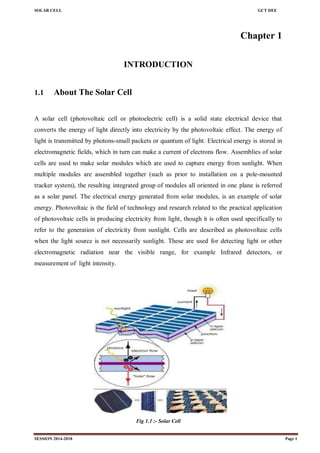
  • 1. SOLAR CELL GCT DEE SESSION 2014-2018 Page 1 Chapter 1 INTRODUCTION 1.1 About The Solar Cell A solar cell (photovoltaic cell or photoelectric cell) is a solid state electrical device that converts the energy of light directly into electricity by the photovoltaic effect. The energy of light is transmitted by photons-small packets or quantum of light. Electrical energy is stored in electromagnetic fields, which in turn can make a current of electrons flow. Assemblies of solar cells are used to make solar modules which are used to capture energy from sunlight. When multiple modules are assembled together (such as prior to installation on a pole-mounted tracker system), the resulting integrated group of modules all oriented in one plane is referred as a solar panel. The electrical energy generated from solar modules, is an example of solar energy. Photovoltaic is the field of technology and research related to the practical application of photovoltaic cells in producing electricity from light, though it is often used specifically to refer to the generation of electricity from sunlight. Cells are described as photovoltaic cells when the light source is not necessarily sunlight. These are used for detecting light or other electromagnetic radiation near the visible range, for example Infrared detectors, or measurement of light intensity. Fig 1.1 :- Solar Cell
  • 2. SOLAR CELL GCT DEE SESSION 2014-2018 Page 2 A solar cell, or photovoltaic cell, is an electrical device that converts the energy of light directly into electricity by the photovoltaic effect, which is a physical and chemical phenomenon. It is a form of photoelectric cell, defined as a device whose electrical characteristics, such as current, voltage, or resistance, vary when exposed to light. Individual solar cell devices can be combined to form modules, otherwise known as solar panels. In basic terms a single junction silicon solar cell can produce a maximum open-circuit voltage of approximately 0.5 to 0.6 volts. Solar cells are described as being photovoltaic, irrespective of whether the source is sunlight or an artificial light. They are used as a photo detector (for example infrared detectors), detecting light or other electromagnetic radiation near the visible range, or measuring light intensity. The operation of a photovoltaic (PV) cell requires three basic attributes:  The absorption of light, generating either electron-hole pairs or excisions.  The separation of charge carriers of opposite types.  The separate extraction of those carriers to an external circuit. In contrast, a solar thermal collector supplies heat by absorbing sunlight, for the purpose of either direct heating or indirect electrical power generation from heat. A "photo electrolytic cell" (photo-electro-chemical cell), on the other hand, refers either to a type of photovoltaic cell (like that developed by Edmond Becquerel and modern dye-sensitized solar cells), or to a device that splits water directly into hydrogen and oxygen using only solar illumination. 1.2 Introduction of Energy 1.2.1 Non-Renewable Energy Non-Renewable energy is energy which is taken from the sources that are available on the earth in limited quantity and will vanish fifty-sixty years from now. Non-renewable sources are not environmental friendly and can have serious affect on our health. They are called non- renewable because they cannot be re-generated within a short span of time. Non-renewable sources exist in the form of fossil fuels, natural gas, oil and coal. According to recent predictions, the inevitable permanent de-cline in the global oil production rate is expected to start within the next 10-20 years. However, the combustion of fossil fuels in the past has already harmful effects on the delicate balance of nature on our planet. Today, about 20 X 1012 kg of carbon dioxide are put into the atmosphere every year, mainly by burning fossil fuel. Today’s plants are unable to absorb this huge amount of extra CO2.
  • 3. SOLAR CELL GCT DEE SESSION 2014-2018 Page 3 1.2.2 Renewable Energy Renewable energy is energy which is generated from natural sources i.e. sun, wind, rain, tides and can be generated again and again as and when required. They are available in plenty and by far most the cleanest sources of energy available on this planet. For e.g.: Energy that we receive from the sun can be used to generate electricity. Similarly, energy from wind, geothermal, biomass from plants, tides can be used this form of energy to another form. Worldwide, oil prices will then rise considerably favouring the introduction of various renewable energy sources such as the direct conversion of solar energy (solar cells), but also others like for example, hydroelectric- and wind-power systems. Renewable energy sources neither run out nor have any significant harmful effects on our environment. Renewable energy is energy that is collected from renewable resources, which are naturally replenished on a human timescale, such as sunlight, wind, rain, tides, waves, and geothermal heat. Renewable energy often provides energy in four important areas: electricity generation, air and water heating & cooling, transportation, and rural (off-grid) energy services. Renewable energy resources exist over wide geographical areas, in contrast to other energy sources, which are concentrated in a limited number of countries. Rapid deployment of renewable energy and energy efficiency is resulting in significant energy security, climate change mitigation, and economic benefits. The results of a recent review of the literature concluded that as greenhouse gas (GHG) emitters begin to be held liable for damages resulting from GHG emissions resulting in climate change, a high value for liability mitigation would provide powerful incentives for deployment of renewable energy technologies. In international public opinion surveys there is strong support for promoting renewable sources such as solar power and wind power. At the national level, at least 30 nations around the world already have renewable energy contributing more than 20 percent of energy supply. National renewable energy markets are projected to continue to grow strongly in the coming decade and beyond.
  • 4. SOLAR CELL GCT DEE SESSION 2014-2018 Page 4 1.3 Solar Energy Solar energy, radiant light and heat from the sun, is harnessed using a range of ever-evolving technologies such as solar heating, concentrated solar power (CSP), concentrator photovoltaic (CPV), solar architecture and artificial photosynthesis. Solar technologies are broadly characterized as either passive solar or active solar depending on the way they capture, convert and distribute solar energy. Passive solar techniques include orienting a building to the Sun, selecting materials with favourable thermal mass or light dispersing properties, and designing spaces that naturally circulate air. Active solar technologies encompass solar thermal energy, using solar collectors for heating, and solar power, converting sunlight into electricity either directly using photovoltaic (PV), or indirectly using concentrated solar power (CSP). A photovoltaic system converts light into electrical direct current (DC) by taking advantage of the photoelectric effect. Solar PV has turned into a multi-billion, fast-growing industry, continues to improve its cost-effectiveness, and has the most potential of any renewable technologies together with CSP. Concentrated solar power (CSP) systems use lenses or mirrors and tracking systems to focus a large area of sunlight into a small beam. Commercial concentrated solar power plants were first developed in the 1980s. CSP-Stirling has by far the highest efficiency among all solar energy technologies. In 2011, the International Energy Agency said that "the development of affordable, inexhaustible and clean solar energy technologies will have huge longer-term benefits. It will increase countries' energy security through reliance on an indigenous, inexhaustible and mostly import-independent resource, enhance sustainability, reduce pollution, lower the costs of mitigating climate change, and keep fossil fuel prices lower than otherwise. These advantages are global. Hence the additional costs of the incentives for early deployment should be considered learning investments; they must be wisely spent and need to be widely shared".[48] Italy has the largest proportion of solar electricity in the world, in 2015 solar supplied 7.8% of electricity demand in Italy. In 2016, after another year of rapid growth, solar generated 1.3% of global power.
  • 5. SOLAR CELL GCT DEE SESSION 2014-2018 Page 5 1.4 History and Development of Solar Cell Technology The development of solar cell technology began with the 1839 research of French physicist Antoine-César Becquerel. Becquerel observed the photovoltaic effect while experimenting with a solid electrode in an electrolyte solution when he saw a voltage develop when light fell upon the electrode. The major events are discussed briefly below, and other milestones can be accessed by clicking on the image shown below. Charles Fritts - First Solar Cell: The first genuine solar cell was built around 1883 by Charles Fritts, who used junctions formed by coating selenium (a semiconductor) with an extremely thin layer of gold. The device was only about 1 percent efficient. Albert Einstein - Photoelectric Effect: Albert Einstein explained the photoelectric effect in 1905 for which he received the Nobel Prize in Physics in 1921. Russell Ohl - Silicon Solar Cell: Early solar cells, however, had energy conversion efficiencies of under one percent. In 1941, the silicon solar cell was invented by Russell Ohl. Gerald Pearson, Calvin Fuller and Daryl Chapin - Efficient Solar Cells: In 1954, three American researchers, Gerald Pearson, Calvin Fuller and Daryl Chapin, designed a silicon solar cell capable of a six percent energy conversion efficiency with direct sunlight. They created the first solar panels. The photovoltaic effect was experimentally demonstrated first by French physicist Edmond Becquerel. In 1839, at age 19, he built the world's first photovoltaic cell in his father's laboratory. Willoughby Smith first described the "Effect of Light on Selenium during the passage of an Electric Current" in a 20 February 1873 issue of Nature. In 1883 Charles Fritts built the first solid state photovoltaic cell by coating the semiconductor selenium with a thin layer of gold to form the junctions; the device was only around 1% efficient. In 1888 Russian physicist Aleksandr Stoletov built the first cell based on the outer photoelectric effect discovered by Heinrich Hertz in 1887. In 1905 Albert Einstein proposed a new quantum theory of light and explained the photoelectric effect in a landmark paper, for which he received the Nobel Prize in Physics in 1921. Russell Ohl patented the modern junction semiconductor solar cell in 1946[8] while working on the series of advances that would lead to the transistor.
  • 6. SOLAR CELL GCT DEE SESSION 2014-2018 Page 6 Chapter 2 PRINCIPLE OF SOLAR CELL 2.1 About Solar Cell Solar cells are devices which convert solar energy directly into electricity, either directly via the photovoltaic effect, or indirectly by first converting the solar energy to heat or chemical energy. Assemblies of cells used to make solar modules which are used to capture energy from sunlight, are known as solar panels. The energy generated from these solar modules, referred to as solar power. Cells are described as photovoltaic cells when the light source is not necessarily sunlight (lamplight, artificial light etc). The amount of power available from a PV device is determined by -the type and area of the material, the intensity of the sun light , the wavelength of the sunlight. 2.1.1 Theory The solar cell work in several steps  Photons in sunlight hit the solar panel and are absorbed by semiconducting material such as silicon.  An array of solar cells converts solar energy into a usable amount of direct current (DC) electricity. Fig 2.1 :- Working mechanism of solar cell
  • 7. SOLAR CELL GCT DEE SESSION 2014-2018 Page 7  Electrons are excited from their current molecular/atomic orbital. Once excited an electron can either dissipate the energy as heat and return to its orbital or travel through the cell until it reaches an electrode. Current flows through the material to cancel the potential and this electricity is captured. The chemical bonds of the material are vital for this process to work, and usually silicon is used in two layers, one layer being doped with boron, the other phosphorus. These layers have different chemical electric charges and subsequently both drive and direct the current of electrons.  An inverter can convert the power to alternating current (AC). The most commonly known solar cell is configured as a large-area p–n junction made from silicon. Other possible solar cell types are organic solar cells, dye sensitized solar cells, perovskite solar cells, quantum dot solar cells etc. The illuminated side of a solar cell generally have a transparent conducting film for allowing light to enter into active material and to collect the generated charge carriers. Typically, films with high transmittance and high electrical conductance such as indium tin oxide, conducting polymers or conducting nanowire networks are used for the purpose. 2.2 Solar Cell There are several types of solar cells. However, more than 90 % of the solar cells currently made worldwide consist of wafer-based silicon cells. They are either cut from a single crystal rod or from a block composed of many crystals and are correspondingly called mono- crystalline or multi-crystalline silicon solar cells. Wafer-based silicon solar cells are approximately 200 μm thick. Another important family of solar cells is based on thin-films, which are approximately 1-2 μm thick and therefore require significantly less active, semiconducting material. Thin-film solar cells can be manufactured at lower cost in large production quantities; hence their market share will likely increase in the future. However, they indicate lower efficiencies than wafer-based silicon solar cells, which means that more exposure surface and material for the installation is required for a similar performance. A number of solar cells electrically connected to each other and mounted in a single support structure or frame is called a ‘photovoltaic module’. Modules are designed to supply electricity at a certain voltage, such as a common 12 volt system. The current produced is directly dependent on the intensity of light reaching the module. Several modules can be wired together to form an array. Photovoltaic modules and arrays produce direct-current electricity.
  • 8. SOLAR CELL GCT DEE SESSION 2014-2018 Page 8 2.3 Types of Solar Cell Based on the material used different types of solar cell are Fig 2.2 :- Types of Solar cell Materials presently used for photovoltaic solar cells include monocrystalline silicon, polycrystalline silicon, amorphous silicon, cadmium telluride, and copper indium gallium selenide. Many currently available solar cells are made from bulk materials that are cut into wafers between 180 to 240 micrometers thick that are then processed like other semiconductors. Other materials are made as thin-films layers, organic dyes, and organic polymers that are deposited on supporting substrates. A third group are made from nanocrystals and used as quantum dots (electron-confined nanoparticles). Silicon remains the only material that is well-researched in both bulk and thin-film forms. In international public opinion surveys there is strong support for promoting renewable sources such as solar power and wind power. When multiple modules are assembled together (such as prior to installation on a pole-mounted tracker system), the resulting integrated group of modules all oriented in one plane is referred as a solar panel. The electrical energy generated from solar modules, is an example of solar energy. At the national level, at least 30 nations around the world already have renewable energy contributing more than 20 percent of energy supply.
  • 9. SOLAR CELL GCT DEE SESSION 2014-2018 Page 9 Some Other Types of Solar Cell A solar cell (also called photovoltaic cell or photoelectric cell) is a solid state electrical device that converts the energy of light directly into electricity by the photovoltaic effect. The following are the different types of solar cells  Amorphous Silicon solar cell (a-Si)  Biohybrid solar cell  Cadmium telluride solar cell (CdTe)  Concentrated PV cell (CVP and HCVP)  Copper indium gallium selenide solar cells (CI(G)S)  Crystalline silicon solar cell (c-Si)  Dye-sensitized solar cell (DSSC)  Gallium arsenide germanium solar cell (GaAs)  Hybrid solar cell  Luminescent solar concentrator cell (LSC)  Micromorph (tandem-cell using a-Si/μc-Si)  Monocrystalline solar cell (mono-Si)  Multi-junction solar cell (MJ)  Nanocrystal solar cell  Organic solar cell (OPV)  Perovskite solar cell  Photoelectrochemical cell (PEC)  Plasmonic solar cell  Polycrystalline solar cell (multi-Si)  Quantum dot solar cell  Solid-state solar cell  Thin-film solar cell (TFSC)  Wafer solar cell, or wafer-based solar cell crystalline.
  • 10. SOLAR CELL GCT DEE SESSION 2014-2018 Page 10 2.4 Solar Cell Working The solar cell works in following steps: 1. Photons in sunlight hit the solar panel and are absorbed by semiconducting materials, such as silicon. Photons with energy equal to the band gap energy are absorbed to create free electrons. Photons with less energy than the band gap energy pass through the material. 2. Formation of electron-hole pair (exciton). 3. Exciton diffusion to Junction. 4. Charge separation- Electrons (negatively charged) are knocked loose from their atoms, causing an electric potential difference. Current starts flowing through the material to cancel the potential and this electricity is captured i.e. Electrons that are created on the n-type side may travel through the wire, power the load, and continue through the wire until they reach the p-type semiconductor-metal contact. Here, they recombine with a hole that was either created as an electron-hole pair on the p-type side of the solar cell. Due to the special composition of solar cells, the electrons are only allowed to move in a single direction. 5. An array of solar cells converts solar energy into a usable amount of direct current (DC) electricity. 2.4.1 Equivalent Circuit of a Solar Cell Fig 2.3 :- Circuit diagram of Solar cell Fig 2.4:- Symbol of Solar Cell
  • 11. SOLAR CELL GCT DEE SESSION 2014-2018 Page 11 To understand the electronic behavior of a solar cell, it is useful to create a model which is electrically equivalent, and is based on discrete ideal electrical components whose behavior is well defined. An ideal solar cell may be modelled by a current source in parallel with a diode; in practice no solar cell is ideal, so a shunt resistance and a series resistance component are added to the model. The resulting equivalent circuit of a solar cell is shown on the left. Also shown, on the right, is the schematic representation of a solar cell for use in circuit diagrams. 2.4.2 Characteristic Equation From the equivalent circuit it is evident that the current produced by the solar cell is equal to that produced by the current source, minus that which flows through the diode, minus that which flows through the shunt resistor. where  I = output current (ampere)  IL = photogenerated current (ampere)  ID = diode current (ampere)  ISH = shunt current (ampere). The current through these elements is governed by the voltage across them: where  Vj = voltage across both diode and resistor RSH (volt)  V = voltage across the output terminals (volt)  I = output current (ampere)  RS = series resistance (Ω). By the Shockley diode equation, the current diverted through the diode is: where  I0 = reverse saturation current (ampere)  n = diode ideality factor (1 for an ideal diode)  q = elementary charge  k = Boltzmann's constant An alternative derivation produces an equation similar in appearance, but with V on the left- hand side. The two alternatives are identities; that is, they yield precisely the same results. Since the parameters I0, n, RS, and RSH cannot be measured directly.
  • 12. SOLAR CELL GCT DEE SESSION 2014-2018 Page 12 2.5 Efficiency Electrical efficiency (also called conversion efficiency) is a contributing factor in the selection of a photovoltaic system. However, the most efficient solar panels are typically the most expensive, and may not be commercially available. Therefore, selection is also driven by cost efficiency and other factors. The electrical efficiency of a PV cell is a physical property which represents how much electrical power a cell can produce for a given insolation. The basic expression for maximum efficiency of a photovoltaic cell is given by the ratio of output power to the incident solar power (radiation flux times area). The efficiency is measured under ideal laboratory conditions and represents the maximum achievable efficiency of the PV material. Actual efficiency is influenced by the output Voltage, current, junction temperature, light intensity and spectrum. The most efficient type of solar cell to date is a multi-junction concentrator solar cell with an efficiency of 46.0% produced by Fraunhofer ISE in December 2014. The highest efficiencies achieved without concentration include a material by Sharp Corporation at 35.8% using a proprietary triple-junction manufacturing technology in 2009, and Boeing Spectrolab (40.7% also using a triple-layer design). The US company SunPower produces cells that have an efficiency of 21.5%, well above the market average of 12–18%. There is an ongoing effort to increase the conversion efficiency of PV cells and modules, primarily for competitive advantage. In order to increase the efficiency of solar cells, it is important to choose a semiconductor material with an appropriate band gap that matches the solar spectrum. This will enhance the electrical and optical properties. Improving the method of charge collection is also useful for increasing the efficiency. There are several groups of materials that are being developed. Ultrahigh-efficiency devices (η>30%) are made by using GaAs and GaInP2 semiconductors with multi junction tandem cells. High-quality, single- crystal silicon materials are used to achieve high-efficiency, low cost cells (η>20%).
  • 13. SOLAR CELL GCT DEE SESSION 2014-2018 Page 13 Chapter 3 MANUFACTURING OF SOLAR CELL 3.1 Manufacturing Technology and process of Solar Cell 3.1.1 Purification of Silicon Fig 3.1 :- Purification of Silicon The basic component of a solar cell is intrinsic silicon, which is not pure in its natural state. To make solar cells, the raw materials—silicon dioxide of either quartzite gravel or crushed quartz—are first placed into an electric arc furnace, where a carbon arc is applied to release the oxygen. A Graphite and Thermal insulator trap the heat and maintain the furnace at required temperature for gangue (impurity) to form a slag. The products are carbon dioxide and molten silicon. Silicon ingot is pulled down from the molten silicon using seed silicon crystallization and floating zone technique. Passing impure silicon in same direction several times that separates impurities- and impure end is later removed. This process yields silicon with one percent impurity, useful in many industries but not the solar cell industry. At this point, the silicon is still not pure enough to be used for solor cells and requires further purification. Pure silicon is derived from such silicon dioxides as quartzite gravel (the purest silica) or crushed quartz.
  • 14. SOLAR CELL GCT DEE SESSION 2014-2018 Page 14 3.1.2 Ingot and Wafer Preparation Fig 2.4 :- System of Ingot and Wafer Preparation Solar cells are made from silicon boules, polycrystalline structures that have the atomic structure of a single crystal. The most commonly used process for creating the boule is called the Czochralski method. In this process, a seed crystal of silicon is dipped into melted polycrystalline silicon. As the seed crystal is withdrawn and rotated, a cylindrical ingot or "boule" of silicon is formed. The ingot withdrawn is unusually pure, because impurities tend to remain in the liquid. From the boule, silicon wafers are sliced one at a time using a circular saw whose inner diameter cuts into the rod, or many at once with a multi wire saw. (A diamond saw produces cuts that are as wide as the wafer—. 5 millimeter thick.). Only about one-half of the silicon is lost from the boule to the finished circular wafer—more if the wafer is then cut to be rectangular or hexagonal. Only about one-half of the silicon is lost from the boule to the finished circular wafer—more if the wafer is then cut to be rectangular or hexagonal. Rectangular or hexagonal wafers are sometimes used in solar cells because they can be fitted together perfectly, thereby utilizing all available space on the front surface of the solar cell. The wafers are then polished to remove saw marks.
  • 15. SOLAR CELL GCT DEE SESSION 2014-2018 Page 15 3.1.3 Doping The traditional way of doping silicon wafers with boron and phosphorous is to introduce a small amount of boron during the Czochralski process. The wafers are then sealed back to back and placed in a furnace to be heated to slightly below the melting point of silicon (2,570 degrees Fahrenheit or 1,410 degrees Celsius) in the presence of phosphorous gas. The phosphorous atoms "burrow" into the silicon, which is more porous because it is close to becoming a liquid. The temperature and time given to the process is carefully controlled to ensure a uniform junction of proper depth. These diffusion processes are usually performed through the use of a batch tube furnace or an in-line continuous furnace. The basic furnace construction and process are very similar to the process steps used by packaging engineers. 3.1.4 Screen Printing Fig 2.5 :- View of Screen Printing of Solar Cell Electrical contacts are formed through squeezing a metal paste through mesh screens to create a metal grid. This metal paste (usually Ag or Al) needs to be dried so that subsequent layers can be screen-printed using the same method. It is predicted that second generation cells will dominate the residential solar market. This electric field acts as a diode, allowing (and even pushing) electrons to flow from the P side to the N side. As a last step, the wafer is heated in a continuous firing furnace at temperatures ranging from 780 to 900°C. These grid- pattern metal screens act as collector electrodes that carry electrons and complete the electrical continuity in the circuit.
  • 16. SOLAR CELL GCT DEE SESSION 2014-2018 Page 16 2.3.5 Stringing And Tabbing Fig 2.6 :- View of Stringing and Tabbing Electrical contacts connect each solar cell to another and to the receiver of produced current. The contacts must be very thin (at least in the front) so as not to block sunlight to the cell electrical use. There are also many rebates available to help you save 40-60% on the cost of acquiring your system. This causes further disruption of electrical neutrality. if an external current path is provided, electrons will flow through the path to the P side to unite with holes that the electric field sent there, doing work for us along the way. The outer shell, however, is only half full with just four electrons (Valence electrons). The electron flow provides the current, and the cell's electric field causes a voltage. Instead of having free electrons, P-type ("p" for positive) has free openings and carries. the heat and maintain the furnace at required temperature for gangue (impurity) to form a slag. The products are carbon dioxide and molten silicon. Silicon ingot is pulled down from the molten silicon using seed silicon crystallization and floating zone technique. For more information on rebates and incentives for installing a solar power system on your home or business look up "Energy Incentives" on the IRS website or check with your local tax adviser for details. Metals such as palladium/silver, nickel, or copper are vacuum-evaporated After the contacts are in place, thin strips ("fingers") are placed between cells. The most commonly used strips are tin-coated copper.
  • 17. SOLAR CELL GCT DEE SESSION 2014-2018 Page 17 3.1.6 Antireflective Coating Because pure silicon is shiny, it can reflect up to 35 percent of the sunlight. To reduce the amount of sunlight lost, an anti-reflective coating is put on the silicon wafer- mostly titanium dioxide, silicon oxide and some others are used. The material used for coating is either heated until its molecules boil off and travel to the silicon and condense, or the material undergoes sputtering. In this process, a high voltage knocks molecules off the material and deposits them onto the silicon at the opposite electrode. Yet another method is to allow the silicon itself to react with oxygen- or nitrogen-containing gases to form silicon dioxide or silicon nitride. Commercial solar cell manufacturers use silicon nitride. Another method to make silicon absorb more light is to make its top surface grained, i.e. pyramid shaped nanostructures that yield 70% absorption that reaches the cell surface after passing through anti-reflective coating. Fig 2.7 :- Antireflective Coating on Solar Cell 3.1.7 Module Manufacturing The finished solar cells are then encapsulated; that is, sealed into silicon rubber or ethylene vinyl acetate. Solar module assembly usually involves soldering cells together to produce a 36- cell string (or longer) and laminating it between toughened glass on the top and a polymeric backing sheet on the bottom. The encapsulated solar cells are then placed into an aluminum frame that has a Mylar or tedlar back sheet and a glass or plastic cover. Frames are usually applied to allow for mounting in the field, or the laminates may be separately integrated into a mounting system for a specific application such as integration into a building.
  • 18. SOLAR CELL GCT DEE SESSION 2014-2018 Page 18 Chapter 4 MATERIAL USE IN SOLAR CELL 4.1 Materials Used in Solar Cell Various materials display varying efficiencies and have varying costs. Materials for efficient solar cells must have characteristics matched to the spectrum of available light. Some cells are designed to efficiently convert wavelengths of solar light that reach the Earth surface. However, some solar cells are optimized for light absorption beyond Earth's atmosphere as well. Light absorbing materials can often be used in multiple physical configurations to take advantage of different light absorption and charge separation mechanisms. Materials presently used for photovoltaic solar cells include monocrystalline silicon, polycrystalline silicon, amorphous silicon, cadmium telluride, and copper indium selenide/sulfide. Many currently available solar cells are made from bulk materials that are cut into wafers between 180 to 240 micrometers thick that are then processed like other semiconductors. 4.1.1 Crystalline Silicon By far, the most prevalent bulk material for solar cells is crystalline silicon (abbreviated as a group as c-Si), also known as "solar grade silicon". Bulk silicon is separated into multiple categories according to crystallinity and crystal size in the resulting ingot, ribbon, or wafer. Fig 4.1 :- Crystalline silicon
  • 19. SOLAR CELL GCT DEE SESSION 2014-2018 Page 19 a.) Monocrystalline Silicon (C-Si): often made using the Czochralski process. Singlecrystal wafer cells tend to be expensive, and because they are cut from cylindrical ingots, do not completely cover a square solar cell module without a substantial waste of refined silicon. Hence most c-Si panels have uncovered gaps at the four corners of the cells. b.) Polycrystalline Silicon & Multicrystalline Silicon, (Poly-Si Or Mc-Si): made from cast square ingots — large blocks of molten silicon carefully cooled and solidified. Poly- Si cells are less expensive to produce than single crystal silicon cells, but are less efficient. United States Department of Energy data show that there were a higher number of polycrystalline sales than monocrystalline silicon sales. c.) Ribbon Silicon: It is a type of polycrystalline silicon. it is formed by drawing flat thin films frommolten silicon and results in a polycrystalline structure. These cells have lower efficiencies than poly-Si, but save on production costs due to a great reduction in silicon waste, as this approach does not require sawing from ingots. d.) Mono Si & Multi Silicon: Developed in the 2000s and introduced commercially around 2009, mono-like-multi, or cast-mono, uses existing polycrystalline casting chambers with small "seeds" of mono material. The result is a bulk mono-like material with poly around the outsides. When sawn apart for processing, the inner sections are high-efficiency mono-like cells (but square instead of "clipped"), while the outer edges are sold off as conventional poly. The result is line that produces mono-like cells at poly- like prices. 4.1.2 Thin films Thin-film technologies reduce the amount of material required in creating the active material of solar cell. Most thin film solar cells are sandwiched between two panes of glass to make a module. Since silicon solar panels only use one pane of glass, thin film panels are approximately twice as heavy as (A-Si) are three thin-film technologies often used as outdoor photovoltaic solar power production. CdTe technology is most cost competitive among them. Silicon thin-film cells are mainly deposited by chemical vapor deposition (typically plasma- enhanced, PE-CVD) from silane gas and hydrogen gas. Depending on the deposition parameters, this can yield amorphous silicon (a-Si or a-Si:H), protocrystalline silicon or nanocrystalline silicon (nc-Si or nc-Si:H), also called microcrystalline silicon. Amorphous silicon is the most well-developed thin film technology to-date. An amorphous silicon (a-Si) solar cell is made of non-crystalline or microcrystalline silicon.
  • 20. SOLAR CELL GCT DEE SESSION 2014-2018 Page 20 4.1.3 Cadmium Telluride Solar Cell A cadmium telluride solar cell uses a cadmium telluride (CdTe) thin film, a semiconductor layer to absorb and convert sunlight into electricity. Solarbuzz has reported that the lowest quoted thin-film module price stands at US$0.84 per watt-peak, with the lowest crystalline silicon (c-Si) module at $1.06 per watt-peak. 4.1.4 Copper Indium Gallium Selenide Copper indium gallium selenide (CIGS) is a direct band gap material. It has the highest efficiency (~20%) among thin film materials (see CIGS solar cell). Traditional methods of fabrication involve vacuum processes including co-evaporation and sputtering. Recent developments at IBM and Nanosolar attempt to lower the cost by using non-vacuum solution processes. Amorphous silicon has a higher bandgap (1.7 eV) than crystalline silicon (c-Si) (1.1 eV), which means it absorbs the visible part of the solar spectrum more strongly than the higher power density infrared portion of the spectrum. The production of a-Si thin film solar cells uses glass as a substrate and deposits a very thin layer of silicon by plasma-enhanced chemical vapor deposition (PECVD). 4.1.5 Gallium Arsenide Multijunction High-efficiency multijunction cells were originally developed for special applications such as satellites and space exploration, but at present, their use in terrestrial concentrators might be the lowest cost alternative in terms of $/kWh and $/W. These multijunction cells consist of multiple thin films produced using metalorganic vapour phase epitaxy. A triple-junction cell, for example, may consist of the absorb electromagnetic radiation over a portion of the spectrum. Combinations of semiconductors are carefully chosen to absorb nearly all of the solar spectrum, thus generating electricity from as much of the solar energy as possible. GaAs based multijunction devices are the most efficient solar cells to date. In 15 October 2012, triple junction metamorphic cell reached a record high of 44%. Tandem solar cells based on monolithic, series connected, gallium indium phosphide (GaInP), gallium arsenide GaAs, and germanium Ge p–n junctions, are seeing demand rapidly rise. Between December 2006 and December 2007, the cost of 4N gallium metal rose from about $350 per kg to $680 per kg. Additionally, germanium metal prices have rise substantially to $1000–1200 per kg this year.
  • 21. SOLAR CELL GCT DEE SESSION 2014-2018 Page 21 4.1.6 Light-Absorbing Dyes (DSSC) Dye-sensitized solar cells (DSSCs) are made of low-cost materials and do not need elaborate equipment to manufacture, so they can be made in a DIY fashion, possibly allowing players to produce more of this type of solar cell than others. In bulk it should be significantly less expensive than older solid-state cell designs. DSSC's can be engineered into flexible sheets, and although its conversion efficiency is less than the best thin film cells, its price to compete with fossil fuel electrical generation. Typically a ruthenium metal organic dye (Ru-centered) is used as a monolayer of light absorbing material. The dye-sensitized solar cell depends on a mesoporous layer of an titanium dioxide to greatly amplify the surface area (200–300 m2/g TiO2, as compared to approximately 10 m2/g of flat single crystal). 4.1.7 Quantum Dot Solar Cells (QDSCs) Quantum dot solar cells (QDSCs) are based on the Gratzel cell, or dye-sensitized solar cell, architecture but employ low band gap semiconductor nanoparticles, fabricated with such small crystallite sizes that they form quantum dots (such as CdS, CdSe, Sb2S3, PbS, etc.), instead of organic or organometallic dyes as light absorbers. Quantum dots (QDs) have attracted much interest because of their unique properties. Their size quantization allows for the band gap to be tuned by simply changing particle size. They also have high extinction coefficients, and have shown the possibility of multiple exciton generation. 4.1.8 Organic/Polymer Solar Cells Organic solar cells are a relatively novel technology, yet hold the promise of a substantial price reduction (over thin-film silicon) and a faster return on investment. These cells can be processed from solution, hence the possibility of a simple roll-to-roll printing process, leading to inexpensive, large scale production. Organic solar cells and polymer solar cells are built from thin films (typically 100 nm) of organic semiconductors including polymers, such as poly phenyl and small molecule compounds like copper phthalocyanine PCBM. Energy conversion efficiencies achieved to date using conductive polymers are low compared to inorganic materials. Protocrystalline silicon with a low volume fraction of nanocrystalline silicon is optimal for high open circuit voltage.[60] Nc-Si has about the same bandgap as c-Si and nc-Si and a-Si can advantageously be combined in thin layers, creating a layered cell called a tandem cell. The top cell in a-Si absorbs the visible light and leaves the infrared part of the spectrum for the bottom cell in nc-Si.
  • 22. SOLAR CELL GCT DEE SESSION 2014-2018 Page 22 4.1.9 Silicon Thin Films Silicon thin-film cells are mainly deposited by chemical vapor deposition (typically plasmaenhanced, PE-CVD) from silane gas and hydrogen gas. Depending on the deposition parameters, this can yield: 1. Amorphous Silicon (A-Si Or A-Si:H) 2. Protocrystalline Silicon 3. Nanocrystalline Silicon (Nc-Si Or Nc-Si:H) & Microcrystalline Silicon. An amorphous silicon (a-Si) solar cell is made of amorphous or microcrystalline silicon and its basic electronic structure is the p-i-n junction. a-Si is attractive as a solar cell material because it is abundant and non-toxic (unlike its CdTe counterpart) and requires a low processing temperature, enabling production of devices to occur on flexible and low-cost substrates. As the amorphous structure has a higher absorption rate of light than crystalline cells, the complete light spectrum can be absorbed with a very thin layer of photo-electrically active material. A film only 1 micron thick can absorb 90% of the usable solar energy. This reduced material requirement along with current technologies being capable of large-area deposition of a-Si, the scalability of this type of cell is high. Recently, solutions to overcome the limitations of thin-film crystalline silicon have been developedAnti-reflective coatings can also be applied to create destructive interference within the cell. This can be done by modulating the Refractive index of the surface coating; if destructive interference is achieved, there will be no reflective wave and thus all light will be transmitted into the semiconductor cell. This can be achieved by adding a textured backreflector to the nanowire arrays enables long absorption lengths along the length of the wire while still maintaining short minority carrier diffusion lengths along the radial direction. Adding nanoparticles between the nanowires will allow for conduction through the device. Because of the natural geometry of these arrays, a textured surface will naturallwhich allows for even more light to be trapped. A further advantage of this geometry is that these types of devices require about 100 times less material than conventional wafer-based devices.
  • 23. SOLAR CELL GCT DEE SESSION 2014-2018 Page 23 4.2 Materials Fig 4.2 :- Glabal market-share in term of annual production Solar cells are typically named after the semiconducting material they are made of. These materials must have certain characteristics in order to absorb sunlight. Some cells are designed to handle sunlight that reaches the Earth's surface, while others are optimized for use in space. Solar cells can be made of only one single layer of light-absorbing material (single- junction) or use multiple physical configurations (multi-junctions) to take advantage of various absorption and charge separation mechanisms. Solar cells can be classified into first, second and third generation cells. The first generation cells—also called conventional, traditional or wafer-based cells—are made of crystalline silicon, the commercially predominant PV technology, that includes materials such as polysilicon and monocrystalline silicon. Second generation cells are thin film solar cells, that include amorphous silicon, CdTe and CIGS cells and are commercially significant in utility- scale photovoltaic power stations, building integrated photovoltaics or in small stand-alone power system. The third generation of solar cells includes a number of thin-film technologies often described as emerging photovoltaics—most of them have not yet been commercially applied and are still in the research or development phase. Many use organic materials, often organometallic compounds as well as inorganic substances. Despite the fact that their efficiencies had been low and the stability of the absorber material was often too short for commercial applications, there is a lot of research invested into these technologies as they promise to achieve the goal of producing low-cost, high-efficiency solar cells.
  • 24. SOLAR CELL GCT DEE SESSION 2014-2018 Page 24 Chapter 5 GENERATION OF SOLAR CELL 5.1 First Generation: Crystalline Silicon Solar Cell Technology This term refers to the classics p-n junction photovoltaic. Typically, this is made from silicon (multicrystalline and single crystalline) doped with other elements to make them preferentially positive (p) or negative (n) with respect to electronic charge carriers as shown in figure. However in the past these devices were made from other materials like Germanium as well. First generation photovoltaic cells (also known as silicon wafer-based solar cells) are the dominant technology in the commercial production of solar cells, accounting for more than 86% of the solar cell market. They are dominant due to their high efficiency. This despite their high manufacturing costs, a problem that second generation cells hope to remedy. Monocrystalline silicon (c-Si) often made using the Czochralski process. Single- crystal wafer cells tend to be expensive, and because they are cut from cylindrical ingots, do not completely cover a square solar cell module without a substantial waste of refined silicon. Hence most c-Si panels have uncovered gaps at the four corners of the cells. Monocrystalline solar cells can achieve 17% efficiency. Fig 5.1 :- Silicon Solar cell structure
  • 25. SOLAR CELL GCT DEE SESSION 2014-2018 Page 25 First generation solar cells are the larger, silicon-based photovoltaic cells. Silicon's ability to remain a semiconductor at higher temperatures has made it a highly attractive raw material for solar panels. Silicon's abundance, however, does not ease the challenges of harvesting and processing it into a usable material for microchips and silicon panels. Solar cells, use silicon wafers consisting of Silicon or Germanium that are doped with Phosphorus and Boron in a pn-junction. Silicon cells have a quite high efficiency, but very pure silicon is needed, and due to the energy-requiring process, the price is high compared to the power output. Crystalline Silicon Solar Cells dominate 80-90% of solar cell market due to their high efficiency, despite their high manufacturing costs. 5.2 Second Generation: Thin Film Solar Cell Technology Thin films of photon-absorbers and layered stacks of thin films. It can combine multiple light absorbing materials in a ―stack‖ of films, with each absorbing a slightly different range of light wavelengths than the one below it. The advantage of using a thin-film of material was reducing the mass of material required for cell design. Typically, the efficiencies of thin-film solar cells are lower compared with silicon (wafer-based) solar cells, but manufacturing costs are also lower. The most successful second generation materials have been cadmium telluride (CdTe), copper indium gallium selenide, amorphous silicon and micromorphous silicon. A cadmium telluride solar cell uses a cadmium telluride (CdTe) thin film, a semiconductor layer to absorb and convert sunlight into electricity. The cadmium present in the cells would be toxic if released. CdTe technology costs about 30% less than CIGS technology and 40% less than A-Si technology. Copper indium gallium selenide (CIGS) is a direct band gap material. It has the highest efficiency (~20%) among thin film materials (see CIGS solar cell). An amorphous silicon (a-Si) solar cell is made of amorphous or microcrystalline silicon and its basic electronic structure is the p-i-n junction. a-Si is attractive as a solar cell material because it is abundant and non-toxic (unlike its CdTe counterpart) and requires a low processing temperature, enabling production of devices to occur on flexible and low-cost substrates. As the amorphous structure has a higher absorption rate of light than crystalline cells, the complete light spectrum can be absorbed with a very thin layer of photo-electrically active material. However, because it is amorphous, it has high inherent disorder and dangling bonds, making it a bad conductor for charge carriers.
  • 26. SOLAR CELL GCT DEE SESSION 2014-2018 Page 26 5.3 Third Genaration: Dye-Sensitized Solar Cell Technology Third generation technologies aim to enhance poor electrical performance of second generation (thin-film technologies) while maintaining very low production costs. Generally, third generation cells include solar cells that do not need the p-n junction necessary in traditional semiconductor, silicon-based cells. Third generation contains a wide range of potential solar innovations including polymer solar cells, nanocrystalline cells, and dye-sensitized solar cells. 5.3.1 Dye-Sensitized Solar Cell (DSSC, DSC Or DYSC) It is a low-cost solar cell belonging to the group of thin film solar cells[12]. It is based on a semiconductor formed between a photo-sensitized anode and an electrolyte, a photo electrochemical system. A modern DSSC shown in figure is composed of a porous layer of titanium dioxide nano particles, covered with a molecular dye that absorbs sunlight. The titanium dioxide is immersed under an electrolyte solution, above which is a platinum-based catalyst. As in a conventional alkaline battery, an anode (the titanium dioxide) and a cathode (the platinum) are placed on either side of a liquid conductor (the electrolyte). Sunlight passes through the transparent electrode into the dye layer where it can excite electrons that then flow into the titanium dioxide. The electrons flow toward the transparent electrode where they are collected for powering a load. After flowing through the external circuit, they are re-introduced into the cell on a metal electrode on the back, flowing into the electrolyte. The electrolyte then transports the electrons back to the dye molecules. In the DSSC, the bulk of the semiconductor is used solely for charge transport, the photoelectrons are provided from a separate photosensitive dye. Charge separation occurs at the surfaces between the dye, semiconductor and electrolyte. The dye molecules are quite small (nanometer sized), so in order to capture a reasonable amount of the incoming light the layer of dye molecules needs to be made fairly thick, much thicker than the molecules themselves. To address this problem, a nanomaterial is used as a scaffold to hold large numbers of the dye molecules in a 3-D matrix, increasing the number of molecules for any given surface area of cell. Overall peak power conversion efficiency for current DSSCs is about 11% Current record for prototypes lies at 12.3%.
  • 27. SOLAR CELL GCT DEE SESSION 2014-2018 Page 27 Fig 5.2 :- Dye-Sensitized Solar Cell 5.3.2 Quantum Dot Solar Cells (QDSCs) These are based off of the Gratzel cell, or dye-sensitized solar cell, architecture but employ low band gap semiconductor nanoparticles, also called quantum dots (such as CdS, CdSe, Sb2S3, PbS, etc.), instead of organic or organometallic dyes as light absorbers (nc-Si) has about the same bandgap as c-Si, the nc-Si and a- Si can advantageously be combined in thin layers, creating a layered cell called a tandem cell. The top cell in a-Si absorbs the visible light and leaves the infrared part of the spectrum for the bottom cell in nc-Si. 5.3.3 Organic Solar Cells And Polymer Solar Cells These are built from thin films (typically 100 nm) of organic semiconductors including polymers, such as polyphenylene vinylene and small-molecule compounds like copper phthalocyanine (a blue or green organic pigment) and carbon fullerenes and fullerene derivatives such as PCBM. Energy conversion efficiencies achieved to date using conductive polymers are low compared to inorganic materials. However, it has improved quickly in the last few years and the highest NREL (National Renewable Energy Laboratory) certified efficiency has reached 8.3% for the Konarka Power Plastic[16]. In addition, these cells could be beneficial for some applications where mechanical flexibility and disposability are important. These devices differ from inorganic semiconductor solar cells in that they do not rely on the large built-in electric field of a PN junction to separate the electrons and holes created when photons are absorbed. The active region of an organic device consists of two materials, one which acts as an electron donor and the other as an acceptor. When a photon is converted into an electron hole pair, typically in the donor material, the charges tend to remain bound in the form of an exciton, and are separated when the exciton diffuses to the donor-acceptor interface. excitons are broken up into free electrons-hole pairs by effective fields. The effective field are set up by creating a heterojunction between two dissimilar materials.
  • 28. SOLAR CELL GCT DEE SESSION 2014-2018 Page 28 Fig 5.3 :- Structure of OSC OSC consists of - Organic material is sandwiched between two electrodes, One electrode is transparent, Organic material absorbs/emitts light (OPV/OLED). As shown in figure bilayer OSC structure consists of - Two different organic materials, Exciton dissociation at the interface, Power conversion efficiency > 1% is possible. Structure of bulk heterojunction OSC consists of  Exciton blocking layer  Hole blocking layer  Prevents metal diffusion into acceptor.
  • 29. SOLAR CELL GCT DEE SESSION 2014-2018 Page 29 OSC Advantages  Low temperature, low energy processing  Low material requirement  Relatively cheap in production and purification.  Can be used on flexible substrate.  Materials can be tailored for the demand  Can be shaped or tinted to suit architectural applications.  Low manufacturing cost  Utilization of eco friendly materials  Scalable manufacturing processes for large area Organic solar cells (OSC) are flexible, semi-transparent and relatively inexpensive to produce. OSC Disadvantages  Low efficiency  Unproven technology  Limited lifetime/ stability issue
  • 30. SOLAR CELL GCT DEE SESSION 2014-2018 Page 30 Chapter 6 PHOTOVOLTAIC TECHNOLOGY 6.1 About Photovoltaic Technology Photovoltaic (PV) is a term which covers the conversion of light into electricity using semiconducting materials that exhibit the photovoltaic effect, a phenomenon studied in physics, photochemistry, and electrochemistry. A typical photovoltaic system employs solar panels, each comprising a number of solar cells, which generate electrical power. PV installations may be ground-mounted, rooftop mounted or wall mounted. The mount may be fixed, or use a solar tracker to follow the sun across the sky. Solar PV has specific advantages as an energy source: once installed, its operation generates no pollution and no greenhouse gas emissions, it shows simple scalability in respect of power needs and silicon has large availability in the Earth’s crust. PV systems have the major disadvantage that the power output is dependent on direct sunlight, so about 10-25% is lost if a tracking system is not used, since the cell will not be directly facing the sun at all times. Dust, clouds, and other things in the atmosphere also diminish the power output. Another main issue is the concentration of the production in the hours corresponding to main insolation, which do not usually match the peaks in demand in human activity cycles. Unless current societal patterns of consumption and electrical networks mutually adjust to this scenario, electricity still needs to be stored for later use or made up by other power sources, usually hydrocarbon. Photovoltaic systems have long been used in specialized applications, and standalone and grid- connected PV systems have been in use since the 1990s. They were first mass-produced in 2000, when German environmentalists and the Eurosolarorganization got government funding for a ten thousand roof program. Advances in technology and increased manufacturing scale have in any case reduced the cost, increased the reliability, and increased the efficiency of photovoltaic installations. Net metering and financial incentives, such as preferential feed-in tariffs for solar-generated electricity, have supported solar PV installations in many countries. More than 100 countries now use solar PV.
  • 31. SOLAR CELL GCT DEE SESSION 2014-2018 Page 31 Photovoltaics is the field of technology and research related to the devices which directly convert sunlight into electricity. The solar cell is the elementary building block of the photovoltaic technology. In this situation, a leftward electron current is possible despite an electric field pushing electrons in the opposite direction. However, if when a photon excites an electron, it does not quickly relax back to an immobile state, but instead keeps moving around the crystal and scattering randomly, then the electron will eventually "forget" that it was moving left, and it will wind up being pulled rightward by the electric field. Again, the total leftward motion of an electron, per photon absorbed, cannot be much larger than the mean free path. Solar cells are made of semiconductor materials, such as silicon. One of the properties of semiconductors that makes them most useful is that their conductivity may easily be modified by introducing impurities into their crystal lattice. For instance, in the fabrication of a photovoltaic solar cell, silicon, which has four valence electrons, is treated to increase its conductivity.On one side of the cell, the impurities, which are phosphorus atoms with five valence electrons (n-donor), donate weakly bound valence electrons to the silicon material, creating excess negative charge carriers. On the other side, atoms of boron with three valence electrons (p-donor) create a greater affinity than silicon to attract electrons. Because the p-type silicon is in intimate contact with the n-type silicon a p-n junction is established and a diffusion of electrons occurs from the region of high electron concentration (the n-type side) into the region of low electron concentration (p-type side). When the electrons diffuse across the p-n junction, they recombine with holes on the p-type side. However, the diffusion of carriers does not occur indefinitely, because the imbalance of charge immediately on either sides of the junction originates an electric field. This electric field forms a diode that promotes current to flow in only one direction. Ohmic metal-semiconductor contacts are made to both the n-type and p-type sides of the solar cell, and the electrodes are ready to be connected to an external load. When photons of light fall on the cell, they transfer their energy to the charge carriers. Organic and polymer photovoltaic (OPV) are a relatively new area of research. The tradition OPV cell structure layers consist of a semi-transparent electrode, electron blocking layer, tunnel junction, holes blocking layer, electrode, with the sun hitting the transparent electrode. The electric field across the junction separates photo- generated positive charge carriers (holes) from their negative counterpart (electrons). In this way an electrical current is extracted once the circuit is closed on an external load.
  • 32. SOLAR CELL GCT DEE SESSION 2014-2018 Page 32 6.2 Photovoltaic Effect The photovoltaic effect is the creation of voltage and electric current in a material upon exposure to light and is a physical and chemical property/phenomenon. The photovoltaic effect is closely related to the photoelectric effect. In either case, light is absorbed, causing excitation of an electron or other charge carrier to a higher-energy state. The main distinction is that the term photoelectric effect is now usually used when the electron is ejected out of the material (usually into a vacuum) and photovoltaic effect used when the excited charge carrier is still contained within the material. In either case, an electric potential (or voltage) is produced by the separation of charges, and the light has to have a sufficient energy to overcome the potential barrier for excitation. The physical essence of the difference is usually that photoelectric emission separates the charges by ballistic conduction and photovoltaic emission separates them by diffusion, but some "hot carrier" photovoltaic device concepts blur even this line of distinction. The first solar cell, consisting of a layer of selenium covered with a thin film of gold, was experimented by Charles Fritts in 1884, but it had a very poor efficiency. A demonstration of the photovoltaic effect in 1839 used an electrochemical cell, but the most familiar form of the photovoltaic effect in modern times though is in solid-state devices, mainly in photodiodes. When sunlight or other sufficiently energetic light is incident upon the photodiode, the electrons present in the valence bandabsorb energy and, being excited, jump to the conduction band and become free. These excited electrons diffuse, and some reach the rectifying junction (usually a p-n junction) where they are accelerated into a different material by a built-in potential (Galvani potential). This generates an electromotive force, and thus some of the light energy is converted into electric energy. The photovoltaic effect can also occur when two photons are absorbed simultaneously in a process called two-photon photovoltaic effect. The photovoltaic effect was first observed by French physicist A. E. Becquerel in 1839. He explained his discovery in Les Comptes Rendus de l'Académie des Sciences, "the production of an electric current when two plates of platinum or gold immersed in an acid, neutral, or alkaline solution are exposed in an uneven way to solar radiation”. In most photovoltaic applications the radiation is sunlight, and the devices are called solar cells. In the case of a p-n junction solar cell, illuminating the material creates an electric current as excited electrons and the remaining holes are swept in different directions by the built-in electric field of the depletion region.
  • 33. SOLAR CELL GCT DEE SESSION 2014-2018 Page 33 6.3 Environmental Impacts of Photovoltaic Technologies While solar photovoltaic (PV) cells are promising for clean energy production, their deployment is hindered by production costs, material availability, and toxicity. Data required to investigate their impact are sometimes affected by a rather large amount of uncertainty. The values of human labor and water consumption, for example, are not precisely assessed due to the lack of systematic and accurate analyses in the scientific literature. Life cycle assessment (LCA) is one method of determining environmental impacts from PV. Many studies have been done on the various types of PV including first generation, second generation, and third generation. Usually these PV LCA studies select a cradle to gate system boundary because often at the time the studies are conducted, it is a new technology not commercially available yet and their required balance of system components and disposal methods are unknown. Most LCAs of PV have focused on two categories: carbon dioxide equivalents per kWh and energy pay-back time (EPBT). The EPBT is defined as " the time needed to compensate for the total renewable- and non-renewable- primary energy required during the life cycle of a PV system". 6.3.1 Impacts From First-Generation PV Crystalline silicon modules are the most extensively studied PV type in terms of LCA since they are the most commonly used. Mono-crystalline silicon photovoltaic systems (mono-si) have an average efficiency of 14.0%.[56] The cells tend to follow a structure of front electrode, anti-reflection film, n-layer, p-layer, and back electrode, with the sun hitting the front electrode. EPBT ranges from 1.7 to 2.7 years.[57] The cradle to gate of CO2-eq/kWh ranges from 37.3 to 72.2 grams. Techniques to produce multi-crystalline silicon (multi-si) photovoltaic cells are simpler and cheaper than mono-si, however tend to make less efficient cells, an average of 13.2%.[56] EPBT ranges from 1.5 to 2.6 years.[57] The cradle to gate of CO2-eq/kWh ranges from 28.5 to 69 grams.[58] Some studies have looked beyond EPBT and GWP to other environmental impacts. In one such study, conventional energy mix in Greece was compared to multi-si PV and found a 95% overall reduction in impacts including carcinogens, eco-toxicity, acidification, eutrophication, and eleven others.
  • 34. SOLAR CELL GCT DEE SESSION 2014-2018 Page 34 6.3.2 Impacts From Second Generation Cadmium telluride (CdTe) is one of the fastest-growing thin film based solar cells which are collectively known as second generation devices. This new thin film device also shares similar performance restrictions (Shockley-Queisser efficiency limit) as conventional Si devices but promises to lower the cost of each device by both reducing material and energy consumption during manufacturing. Today the global market share of CdTe is 5.4%, up from 4.7% in 2008.[55] This technology’s highest power conversion efficiency is 21%. The cell structure includes glass substrate (around 2 mm), transparent conductor layer, CdS buffer layer (50– 150 nm), CdTe absorber and a metal contact layer. CdTe PV systems require less energy input in their production than other commercial PV systems per unit electricity production. The average CO2-eq/kWh is around 18 grams (cradle to gate). CdTe has the fastest EPBT of all commercial PV technologies, which varies between 0.3 and 1.2 years. Copper Indium Gallium Diselenide (CIGS) is a thin film solar cell based on the copper indium diselenide (CIS) family of chalcopyrite semiconductors. CIS and CIGS are often used interchangeably within the CIS/CIGS community. The cell structure includes soda lime glass as the substrate, Mo layer as the back contact, CIS/CIGS as the absorber layer, cadmium sulfide (CdS) or Zn (S,OH)x as the buffer layer, and ZnO : Al as the front contact. CIGS is approximately 1/100th the thickness of conventional silicon solar cell technologies. Materials necessary for assembly are readily available, and are less costly per watt of solar cell. CIGS based solar devices resist performance degradation over time and are highly stable in the field. Reported global warming potential impacts of CIGS range from 20.5 – 58.8 grams CO2- eq/kWh of electricity generated for different solar irradiation (1,700 to 2,200 kWh/m2 /y) and power conversion efficiency (7.8 – 9.12%).[63] EPBT ranges from 0.2 to 1.4 years,[61] while harmonized value of EPBT was found 1.393 years.[54] Toxicity is an issue within the buffer layer of CIGS modules because it contains cadmium and gallium.[52][64] CIS modules do not contain any heavy metals. A 2015 review of EPBT from first and second generation PV suggested that there was greater variation in embedded energy than in efficiency of the cells implying that it was mainly the embedded energy that needs to reduce to have a greater reduction in EPBT. One difficulty in determining impacts due to PV is to determine if the wastes are released to the air, water, or soil during the manufacturing phase.
  • 35. SOLAR CELL GCT DEE SESSION 2014-2018 Page 35 6.3.3 Impacts From Third Generation Third-generation PVs are designed to combine the advantages of both the first and second generation devices and they do not have Shockley-Queisser limit, a theoretical limit for first and second generation PV cells. The thickness of a third generation device is less than 1 µm. One emerging alternative and promising technology is based on an organic-inorganic hybrid solar cell made of methylammonium lead halide perovskites. Perovskite PV cells have progressed rapidly over the past few years and have become one of the most attractive areas for PV research. The cell structure includes a metal back contact (which can be made of Al, Au or Ag), a hole transfer layer (spiro-MeOTAD, P3HT, PTAA, CuSCN, CuI, or NiO), and absorber layer (CH3NH3PbIxBr3-x, CH3NH3PbIxCl3-x or CH3NH3PbI3), an electron transport layer (TiO, ZnO, Al2O3 or SnO2) and a top contact layer (fluorine doped tin oxide or tin doped indium oxide). There are a limited number of published studies to address the environmental impacts of perovskite solar cells. The major environmental concern is the lead used in the absorber layer. Due to the instability of perovskite cells lead may eventually be exposed to fresh water during the use phase. These LCA studies looked at human and ecotoxicity of perovskite solar cells and found they were surprisingly low and may not be an environmental issue. Global warming potential of perovskite PVs were found to be in the range of 24–1500 grams CO2-eq/kWh electricity production. Similarly, reported EPBT of the published paper range from 0.2 to 15 years. The large range of reported values high light the uncertainties associated with these studies. Celik et al. (2016) critically discussed the assumptions made in perovskite PV LCA studies. Two new promising thin film technologies are copper zinc tin sulfide (Cu2ZnSnS4 or CZTS), zinc phosphide (Zn3P2) and single-walled carbon nano-tubes (SWCNT). These thin films are currently only produced in the lab but may be commercialized in the future. The manufacturing of CZTS and (Zn3P2) processes are expected to be similar to those of current thin film technologies of CIGS and CdTe, respectively. While the absorber layer of SWCNT PV is expected to be synthesized with CoMoCAT method. by Contrary to established thin films such as CIGS and CdTe, CZTS, Zn3P2, and SWCNT PVs are made from earth abundant, nontoxic materials and have the potential to produce more electricity annually than the current worldwide consumption. While CZTS and Zn3P2 offer good promise for these reasons, the specific environmental implications of their commercial production are not yet known.
  • 36. SOLAR CELL GCT DEE SESSION 2014-2018 Page 36 There are some other effects of photovoltaic system a.) Anomalous Photovoltaic Effect (APE) The anomalous photovoltaic effect (APE), also called (in certain cases) the bulk photovoltaic effect is a type of a photovoltaic effect which occurs in certain semiconductors and insulators. The "anomalous" refers to those cases where the photovoltage (i.e., the open-circuit voltage caused by the light) is larger than the band gap of the corresponding semiconductor. In some cases, the voltage may reach thousands of volts. Unfortunately, although the voltage is unusually high, the short-circuit current is unusually low. Overall, materials that exhibit the anomalous photovoltaic effect have very low power generation efficiencies, and are never used in practical power-generation systems. There are several situations in which APE can arise. First, in polycrystalline materials, each microscopic grain can act as a photovoltaic. Then the grains add in series, so that the overall open-circuit voltage across the sample is large, potentially much larger than the bandgap. Second, in a similar manner, certain ferroelectric materials can develop stripes consisting of parallel ferroelectric domains, where each domain acts like a photovoltaic and each domain wall acts like a contact connecting the adjacent photovoltaics (or vice versa). Third, a perfect single crystal with a non-centrosymmetric structure can develop a giant photovoltage. This is specifically called the bulk photovoltaic effect, and occurs because of non-centrosymmetry. Specifically, the electron processes—photo-excitation, scattering, and relaxation—occur with different probabilities for electron motion in one direction versus the opposite direction. b.) The Dember Effect When photogenerated electrons and holes have different mobilities, a potential difference can be created between the illuminated and non-illuminated faces of a semiconductor slab. Generally this potential is created through the depth of the slab, whether it is a bulk semiconductor or a polycrystalline film. The difference between these cases is that in the latter, a photovoltage can be created in each one of the microcrystallites. As was mentioned above, in the oblique deposition process inclined crystallites are formed in which one face can absorb light more than the other. This may cause a photovoltage to be generated along the film, as well as through its depth. The transfer of carriers at the surface of crystallites is assumed to be hindered by the presence of some unspecified layer with different properties.
  • 37. SOLAR CELL GCT DEE SESSION 2014-2018 Page 37 6.4 The structure transition model This model suggests that when a material crystallizes both in cubic and hexagonal structures, an asymmetric barrier can be formed by a residual dipole layer at the interface between the two structures. A potential barrier is formed due to a combination of the band gap difference and the electric fields produced at the interface. One should remember that this model can be invoked to explain anomalous PV effect only in those materials that can demonstrate two types of crystal structure. 6.4.1 The P-N Junction Model It was suggested by Starkiewicz [3] that the anomalous PV is developed due to a distribution gradient of positive and negative impurity ions through the microcrystallites, with an orientation such as to give a non-zero total photovoltage. This is equivalent to an array of p-n junctions. However, the mechanism by which such p-n junctions may be formed was not explained. 6.4.2 The Surface Photovoltage Model The interface between crystallites may contain traps for charge carriers. This may lead to a surface charge and an opposite space charge region in the crystallites,[12] in case that the crystallites are small enough. Under illumination of the inclined crystallites electron-hole pairs are generated and cause a compensation of the charge in the surface and within the crystallites. There are several aspects of the bulk photovoltaic effect that distinguish it from other kinds of effects: In the power-generating region of the I-V curve (between open-circuit and short- circuit), electrons are moving in the opposite direction that you would expect from the drift- diffusion equation, i.e. electrons are moving towards higher fermi level or holes are moving towards lower fermi level. If it is assumed that the optical absorption depth is much less than the space charge region in the crystallites, then, because of their inclined shape more light is absorbed in one side than in the other. Thus a difference in the reduction of the charge is created between the two sides. This way a photovoltage parallel to the surface is developed in each crystallite.
  • 38. SOLAR CELL GCT DEE SESSION 2014-2018 Page 38 6.5 Importance of Photovoltaic System We believe that solar photovoltaic systems can be a great energy solution for most homeowners. However, they are not the best solution for every homeowner. In talking to experienced solar contractors they estimate that about 15% of homes are not a good fit for a solar PV system. There are a number of scenarios where PV systems are impractical or where other uses of your money would get better results. In order to make a good determination you need to look at both energy generation and energy conservation. Here is a list of scenarios where we think putting in a PV system would be ill advised: a.) Poor Insulation - Many homeowners have homes that are under insulated. There is no point in creating energy using solar panels only to have that very same energy go out through your roof and be wasted. Energy conservation should always come before energy generation so take care of your home's insulation first before you spend any money on a PV system. Once your home is properly insulated and if you have money left over then you can consider a PV system. Also, it is worth noting that increasingly many states will insist that your home be properly insulated before they will provide rebates for photovoltaic systems. b.) Old Roof - Also, if your insulation is good but your roof is on its last legs you probably should consider getting the roof done first so there is a good foundation for the solar panels. If you try to wait a few years and then do your roof then you are going to have to remove all of the solar panels first which can add unnecessary cost. c.) Unavoidable Shade - Solar panels are very durable devices but their performance drops significantly if all or even part of the panel is exposed to direct shade for any length of time. A competent solar contractor can analyze the location where you are thinking of putting your panels using a device called a solar Pathfinder and can tell you what the impact of shade from trees or other buildings might have. If trees are the problem you have the problem is a good bit harder. Some states have begun enforcing the right of one homeowner not to shade out another homeowner's PV system (a right to light so to speak) so there is some chance you can take legal action to remove whatever is shading your property. However, these types of lawsuits are relatively new and it might end up being more hassle than it is worth. Consider using a pole mounted system for holding your solar panels or consider putting the panels on your garage instead of your house. If these are not options then solar PV might not be the best solution for you.
  • 39. SOLAR CELL GCT DEE SESSION 2014-2018 Page 39 d.) The Payback is Too Long - For some homeowners the payback period for solar energy may be too long. This is particularly true in those states that do not provide any incentives for solar energy. If you are not sure if your state provides incentives check out the database at www.dsireusa.org and you can see what incentives they offer. When all is said and done any investment should make good economic sense. Solar has its positives and negatives as an investment. On the negative side the fact that the current administration is in the process of letting the $3000 federal solar incentive lapse. However, there is a chance this will either get overturned or brought back by the next administration. On the positive side of the equation there is the fact that both electric rates and home heating fuel costs are going up rapidly. e.) Insufficient Capital - Sometimes people just cannot afford to put in a complete PV system. A full size system can cost between $15,000 and $50,000 depending upon the size of your home and for many people these days that is just too much money to come up with. One option is to consider getting a loan for the system. A number of states have low interest rate energy loans they can provide to help support the cost of putting in a more panels later. Once you have a basic system installed adding additional panels is relatively easy. We have seen many owners add on to their base system by looking for sales on panels when the opportunity presents itself. Finally, one option you may want to consider is going with a solar thermal system rather than a PV system. Solar thermal systems cost far less than a full-sized PV system and can still provide very significant energy savings. Most cost between $4000 to $6000 and can pay for themselves in just 3-5 years. f.) You Are Planning to Move - This one is just a bit tougher to judge. The question is, if you are only planning on being in your home a short time will you get a good return on an investment in a PV system. In other words will the increase in your sales price be equal to or greater than what you spent on the system. Many of the areas where this appears to the resale value with real estate agents in your local area. House prices are a local phenomenon and what might be a good investment in solar in one area might be a bad investment in another.
  • 40. SOLAR CELL GCT DEE SESSION 2014-2018 Page 40 Chapter 7 SOLAR TRACKER 7.1 About Solar Tracker A solar tracker is a device that orients a payload toward the Sun. Payloads are usually solar panels, parabolic troughs, fresnel reflectors, lenses or the mirrors of a heliostat. For flat-panel photovoltaic systems, trackers are used to minimize the angle of incidence between the incoming sunlight and a photovoltaic panel. This increases the amount of energy produced from a fixed amount of installed power generating capacity. In standard photovoltaic applications, it was predicted in 2008-2009 that trackers could be used in at least 85% of commercial installations greater than one megawatt from 2009 to 2012. However, as of April 2014, there is not any data to support these predictions. In concentrator photovoltaic (CPV) and concentrated solar power (CSP) applications, trackers are used to enable the optical components in the CPV and CSP systems. The optics in concentrated solar applications accept the direct component of sunlight light and therefore must be oriented appropriately to collect energy. Tracking systems are found in all concentrator applications because such systems collect the sun's energy with maximum efficiency when the optical axis is aligned with incident solar radiation. Fig 7.1 :- solar Tracker system
  • 41. SOLAR CELL GCT DEE SESSION 2014-2018 Page 41 7.2 Basic Concept Sunlight has two components, the "direct beam" that carries about 90% of the solar energy, and the "diffuse sunlight" that carries the remainder – the diffuse portion is the blue sky on a clear day, and is a larger proportion of the total on cloudy days. As the majority of the energy is in the direct beam, maximizing collection requires the Sun to be visible to the panels for as long as possible. The energy contributed by the direct beam drops off with the cosine of the angle between the incoming light and the panel. In addition, the reflectance (averaged across all polarizations) is approximately constant for angles of incidence up to around 50°, beyond which reflectance degrades rapidly. For example, trackers that have accuracies of ± 5° can deliver greater than 99.6% of the energy delivered by the direct beam plus 100% of the diffuse light. As a result, high accuracy tracking is not typically used in non-concentrating PV applications. The purpose of a tracking mechanism is to follow the Sun as it moves across the sky. In the following sections, in which each of the main factors are described in a little more detail, the complex path of the Sun is simplified by considering its daily east-west motion separately from its yearly north-south variation with the seasons of the year. 7.3 Solar Energy Intercepted The amount of solar energy available for collection from the direct beam is the amount of light intercepted by the panel. This is given by the area of the panel multiplied by the cosine of the angle of incidence of the direct beam (see illustration above). Or put another way, the losses due to seasonal angle changes is complicated by changes in the length of the day, increasing collection in the summer in northern or southern latitudes. This biases collection toward the summer, so if the panels are tilted closer to the average summer angles. the devices are called solar cells. In the case of a p-n junction solar cell, illuminating the material creates an electric current as excited electrons and the remaining holes are swept in different directions by the built-in electric field of the depletion region. The energy intercepted is equivalent to the area of the shadow cast by the panel onto a surface perpendicular to the direct beam. This cosine relationship is very closely related to the observation formalized in 1760 by Lambert's cosine law. This describes that the observed brightness of an object is proportional to the cosine of the angle of incidence of the light illuminating it.
  • 42. SOLAR CELL GCT DEE SESSION 2014-2018 Page 42 7.3.1 Reflective Losses Fig 7.2 :- Variations of reflectance with angle of incidence Not all of the light intercepted is transmitted into the panel - a little is reflected at its surface. The amount reflected is influenced by both the refractive index of the surface material and the angle of incidence of the incoming light. The amount reflected also differs depending on the polarization of the incoming light. Incoming sunlight is a mixture of all polarizations. Averaged over all polarizations, the reflective losses are approximately constant up to angles of incidence up to around 50° beyond which it degrades rapidly. See for example the left graph. 7.3.2 Daily East-West Motion of The Sun The Sun travels through 360 degrees east to west per day, but from the perspective of any fixed location the visible portion is 180 degrees during an average 1/2 day period (more in spring and summer; less, in fall and winter). Local horizon effects reduce this somewhat, making the effective motion about 150 degrees. In this situation, a leftward electron current is possible despite an electric field pushing electrons in the opposite direction. However, if when a photon excites an electron, it does not quickly relax back to an immobile state, but instead keeps moving around the crystal and scattering randomly, then the electron will eventually "forget" that it was moving left, and it will wind up being pulled rightward by the electric field. Again, the total leftward motion of an electron, per photon absorbed, cannot be much larger than the mean free path. A solar panel in a fixed orientation between the dawn and sunset extremes will see a motion of 75 degrees to either side, and thus, according to the table above, will lose over 75% of the energy in the morning and evening. Rotating the panels to the east and west can help recapture those losses. A tracker that only attempts to compensate for the east-west movement of the Sun is known as a single-axis tracker.
  • 43. SOLAR CELL GCT DEE SESSION 2014-2018 Page 43 7.3.3 Seasonal North-South Motion of The Sun Due to the tilt of the Earth's axis, the Sun also moves through 46 degrees north and south during a year. The same set of panels set at the midpoint between the two local extremes will thus see the Sun move 23 degrees on either side. Thus according to the above table, an optimally aligned single-axis tracker (see polar aligned tracker below) will only lose 8.3% at the summer and winter seasonal extremes, or around 5% averaged over a year. Conversely a vertically or horizontally aligned single-axis tracker will lose considerably more as a result of these seasonal variations in the Sun's path. For example, a vertical tracker at a site at 60° latitude will lose up to 40% of the available energy in summer, while a horizontal tracker located at 25° latitude will lose up to 33% in winter. A tracker that accounts for both the daily and seasonal motions is known as a dual-axis tracker. Generally speaking, the losses due to seasonal angle changes is complicated by changes in the length of the day, increasing collection in the summer in northern or southern latitudes. This biases collection toward the summer, so if the panels are tilted closer to the average summer angles, the total yearly losses are reduced compared to a system tilted at the spring/fall solstice angle (which is the same as the site's latitude). There is considerable argument within the industry whether the small difference in yearly collection between single and dual-axis trackers makes the added complexity of a two-axis tracker worthwhile. A recent review of actual production statistics from southern Ontario suggested the difference was about 4% in total, which was far less than the added costs of the dual-axis systems. This compares unfavourably with the 24-32% improvement between a fixed-array and single-axis tracker.[12][13] Other Factors A.) Clouds The above models assume uniform likelihood of cloud cover at different times of day or year. These excited electrons diffuse, and some reach the rectifying junction (usually a p-n junction) where they are accelerated into a different material by a built-in potential (Galvani potential). This generates an electromotive force, and thus some of the light energy is converted into electric energy. In different climate zones cloud cover can vary with seasons, affecting the averaged performance figures described above. Alternatively, for example in an area where cloud cover on average builds up during the day, there can be particular benefits in collecting morning sun.
  • 44. SOLAR CELL GCT DEE SESSION 2014-2018 Page 44 B.) Atmosphere The distance that sunlight has to travel through the atmosphere increases as the sun approaches the horizon, as the sunlight has to travel diagonally through the atmosphere. As the path length through the atmosphere increases, the solar intensity reaching the collector decreases. This increasing path length is referred to as the air mass (AM) or air mass coefficient, where AM0 is at the top of the atmosphere, AM1 refers to the direct vertical path down to sea-level with Sun overhead, and AM greater than 1 refers to diagonal paths as the Sun approaches the horizon. Interestingly, even though the sun may not feel particularly hot in the early mornings or during the winter months, the diagonal path through the atmosphere has a less than expected impact on the solar intensity. Even when the Sun is only 15° above the horizon the solar intensity can be around 60% of its maximum value, around 50% at 10° and 25% at only 5° above the horizon.[14] Therefore, trackers can deliver benefit by collecting the significant energy available when the Sun is close to the horizon. C.) Solar Cell Efficiency Solar energy efficiency is Of course the underlying power conversion efficiency of a photovoltaic cell has a major influence on the end result, regardless of whether tracking is employed or not. Of particular relevance to the benefits of tracking are the following: D.) Molecular Structure Much research is aimed at developing surface materials to guide the maximum amount of energy down into the cell and minimize reflective losses. E.) Temperature Photovoltaic solar cell efficiency decreases with increasing temperature, at the rate of about 0.4%/°C.[15] For example, 20% higher efficiency at 10 °C in early morning or winter as compared with 60 °C in the heat of the day or summer. Local horizon effects reduce this somewhat, making the effective motion about 10 degrees As a result, most of these electrons break free, and release a lot more free carriers than in pure silicon. The process of adding impurities on purpose is called doping, and when doped with phosphorous. Therefore, trackers can deliver additional benefit by collecting early morning and winter energy when the cells are operating at their highest efficiency.
  • 45. SOLAR CELL GCT DEE SESSION 2014-2018 Page 45 7.4 Types of Solar Collector  Non-Concentrating Flat-Panels  Concentrating Systems Solar collector mounting systems may be fixed (manually aligned) or tracking. Different types of solar collector and their location (latitude) require different types of tracking mechanism. Tracking systems may be configured as:  Fixed collector / moving mirror - i.e. Heliostat  Moving collector 7.4.1 Fixed Collector / Moving Mirror Many collectors cannot be moved, for example high-temperature collectors where the energy is recovered as hot liquid or gas (e.g. steam). Other examples include direct heating and lighting of buildings and fixed in-built solar cookers, such as Scheffler reflectors. In such cases it is necessary to employ a moving mirror so that, regardless of where the Sun is positioned in the sky, the Sun's rays are redirected onto the collector. Due to the complicated motion of the Sun across the sky, and the level of precision required to correctly aim the Sun's rays onto the target, a heliostat mirror generally employs a dual axis tracking system, with at least one axis mechanized. In different applications, mirrors may be flat or concave. 7.4.2 Moving Collector Trackers can be grouped into classes by the number and orientation of the tracker's axes. Compared to a fixed mount, a single axis tracker increases annual output by approximately 30%, and a dual axis tracker an additional 10-20%. Photovoltaic trackers can be classified into two types: standard photovoltaic (PV) trackers and concentrated photovoltaic (CPV) trackers. The tradition OPV cell structure layers consist of a semi-transparent electrode, electron blocking layer, tunnel junction, holes blocking layer, electrode, with the sun hitting the transparent electrode. OPV replaces silver with carbon as an electrode material lowering manufacturing cost and making them more environmentally friendly. OPV are flexible, low weight, and work well with roll-to roll manufacturing for mass production. OPV uses "only abundant elements coupled to an extremely low embodied energy through very low.
  • 46. SOLAR CELL GCT DEE SESSION 2014-2018 Page 46 The processing temperatures using only ambient processing conditions on simple printing equipment enabling energy pay-back times". Current efficiencies range from 1–6.5% however theoretical analyses show promise beyond 10% efficiency. Each of these tracker types can be further categorized by the number and orientation of their axes, their actuation architecture and drive type, their intended applications, their vertical supports and foundation. There are some tracking mount which are following that a.) Non-Tracking Fixed Mount Residential and small-capacity commercial or industrial rooftop solar panels and solar water heater panels are usually fixed, often flush-mounted on an appropriately facing pitched roof. Advantages of fixed mounts over trackers include the following:  Mechanical Advantages: Simple to manufacture, lower installation and maintenance costs.  Wind-loading: it is easier and cheaper to provision a sturdy mount; all mounts other than fixed flush-mounted panels must be carefully designed having regard to wind loading due to greater exposure.  Indirect light: approximately 10% of the incident solar radiation is diffuse light, available at any angle of misalignment with the Sun.  Tolerance to misalignment: effective collection area for a flat-panel is relatively insensitive to quite high levels of misalignment with the Sun – see table and diagram at Basic concept section above – for example even a 25° misalignment reduces the direct solar energy collected by less than 10%. Fixed mounts are usually used in conjunction with non-concentrating systems, however an important class of non-tracking concentrating collectors, of particular value in the 3rd world, are portable solar cookers. if the wastes are released to the air, water, or soil during the manufacturing phase. Research is underway to try to understand emissions and releases during the lifetime of PV systems. Thus the primary benefit of a tracking system is to collect solar energy for the longest period of the day, and with the most accurate alignment as the Sun's position shifts with the seasons.In addition, the greater the level of concentration employed, the more important accurate tracking becomes, because the proportion of energy derived from direct radiation is higher, and the region where that concentrated energy is focused becomes smaller. These utilize relatively low levels of concentration, typically around 2 to 8 Suns and are manually aligned.
  • 47. SOLAR CELL GCT DEE SESSION 2014-2018 Page 47 7.5 Trackers Even though a fixed flat-panel can be set to collect a high proportion of available noon-time energy, significant power is also available in the early mornings and late afternoons[14] when the misalignment with a fixed panel becomes excessive to collect a reasonable proportion of the available energy. For example, even when the Sun is only 10° above the horizon the available energy can be around half the noon-time energy levels (or even greater depending on latitude, season, and atmospheric conditions). 7.5.1 Non Concentrating Photovoltaic (PV) Tracker Photovoltaic panels accept both direct and diffuse light from the sky. The panels on standard photovoltaic trackers gather both the available direct and diffuse light. The tracking functionality in standard photovoltaic trackers is used to minimize the angle of incidence between incoming light and the photovoltaic panel. This increases the amount of energy gathered from the direct component of the incoming sunlight. Renewable energy is derived from natural processes that are replenished constantly. In its various forms, it derives directly from the sun, or from heat generated deep within the earth. They can be connected in both series and parallel electrical arrangements to produce any required voltage and current combination. As a result, most of these electrons break free, and release a lot more free carriers than in pure silicon. The process of adding impurities on purpose is called doping, and when doped with phosphorous, the resulting silicon is called N- type ("n" for negative) because of the prevalence of free electrons. N-type doped silicon is a much better conductor than pure silicon. There are two main types of photovoltaic system. Grid connected systems (on-grid systems) are connected to the grid and inject the electricity into the grid. Included in the definition is electricity and heat generated from solar, wind, ocean, hydropower, biomass, geothermal resources, and bio fuels and hydrogen derived from renewable resources. The losses due to seasonal angle changes is complicated by changes in the length of the day, increasing collection in the summer in northern or southern latitudes. This biases collection toward the summer, so if the panels are tilted closer to the average summer angles. The physics behind standard photovoltaic (PV) trackers works with all standard photovoltaic module technologies. These include all types of crystalline silicon panels (either mono-Si, or multi-Si) and all types of thin film panels (amorphous silicon, CdTe, CIGS, microcrystalline).
  • 48. SOLAR CELL GCT DEE SESSION 2014-2018 Page 48 7.5.2 Concentrator Photovoltaic (CPV) Trackers The optics in CPV modules accept the direct component of the incoming light and therefore must be oriented appropriately to maximize the energy collected. In low concentration applications a portion of the diffuse light from the sky can also be captured. The tracking functionality in CPV modules is used to orient the optics such that the incoming light is focused to a photovoltaic collector. Fig 7.3 :- 3MW CPV Plant using dual axis tracker in India Fig 7.4 :- 200 KW CPV Plant using dual axis tracker in India  CPV modules that concentrate in one dimension must be tracked normal to the Sun in one axis.  CPV modules that concentrate in two dimensions must be tracked normal to the Sun in two axis.
  • 49. SOLAR CELL GCT DEE SESSION 2014-2018 Page 49 a.) Accuracy Requirements The physics behind CPV optics requires that tracking accuracy increase as the systems concentration ratio increases. However, for a given concentration, nonimaging optics provide the widest possible acceptance angles, which may be used to reduce tracking accuracy.[20][21] In typical high concentration systems tracking accuracy must be in the ± 0.1° range to deliver approximately 90% of the rated power output. In low concentration systems, tracking accuracy must be in the ± 2.0° range to deliver 90% of the rated power output. As a result, high accuracy tracking systems are typical. b.) Technologies Supported Concentrated photovoltaic trackers are used with refractive and reflective based concentrator systems. There are a range of emerging photovoltaic cell technologies used in these systems. These range from conventional, crystalline silicon-based photovoltaic receivers to germanium- based triple junction receivers. 7.6 Single Axis Trackers Single axis trackers have one degree of freedom that acts as an axis of rotation. The axis of rotation of single axis trackers is typically aligned along a true North meridian. It is possible to align them in any cardinal direction with advanced tracking algorithms. There are several common implementations of single axis trackers. If this happens close enough to the electric field, or if free electron and free hole happen to wander into its range of influence, the field will send the electron to the N side and the hole to the P side. This causes further disruption of electrical neutrality, and if an external current path is provided, electrons will flow through the path to the P side to unite with holes that the electric field sent there, doing work for us along the way. The outer shell, however, is only half full with just four electrons (Valence electrons). The electron flow provides the current, and the cell's electric field causes a voltage.These include horizontal single axis trackers (HSAT), horizontal single axis tracker with tilted modules (HTSAT), vertical single axis trackers (VSAT), tilted single axis trackers (TSAT) and polar aligned single axis trackers (PSAT). The orientation of the module with respect to the tracker axis is important when modelling performance.