Thyristor
•Download as PPTX, PDF•
1 like•1,934 views

Silicon Controlled Rectifier (SCR) is a unidirectional semiconductor device made of silicon.SCR is a three-terminal, four-layer semiconductor device consisting of alternate layers of p-type and n-type material.

Recommended
More Related Content
What's hot
What's hot (20)
Similar to Thyristor
Similar to Thyristor (20)
More from Vinod Srivastava
Recently uploaded
Recently uploaded (20)
Thyristor
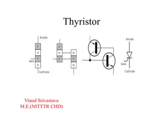
- 2. Introduction Silicon Controlled Rectifier (SCR) is a unidirectional semiconductor device made of silicon. This device is the solid state equivalent of thyratron and hence it is also referred to as thyristor or thyroid transistor. Basically, SCR is a three-terminal, four-layer semiconductor device consisting of alternate layers of p-type and n-type material. Hence it has three pn junctions J1, J2 and J3. The device has terminals Anode(A), Cathode(K) and the Gate(G). The Gate terminal(G) is attached to the p-layer nearer to the Cathode(K) terminal.
- 4. Behavior of Thyristor 1. Reverse Blocking Mode of SCR In this mode, the SCR is reverse biased by connecting its anode terminal (A) to negative end and the cathode terminal (K) to the positive end of the battery. This leads to the reverse biasing of the junctions J1 and J3, which in turn prohibits the flow of current through the device, in spite of the fact that the junction J2 remains in forward biased condition.
- 5. Behavior of Thyristor In this state, the SCR behaves as a typical diode. In this reverse biased condition, only reverse saturation current flows through the device as in the case of the reverse biased diode which is shown in the characteristic curve by blue line. The device also exhibits the reverse breakdown phenomenon beyond a reverse safe voltage limit just like a diode.
- 6. 2. Reverse Conducting Mode: As the reverse voltage is further increased, at the reverse breakdown voltage(VBR) Avalanche breakdown occurs at junction J1 and J3. SCR acts as a closed switch in reverse direction. A large current gives more losses in SCR, dissipating in the form of heat, thereby damaging the SCR.
- 7. 3. Forward Blocking Mode of SCR Here a positive bias is applied to the SCR by connecting anode terminal (A) to the positive and cathode terminal (K) to the negative terminal of the battery, as shown in the figure below. Under this condition, the junction J1 and J3 get forward biased while junction J2 gets reverse biased. Here also current cannot pass through the thyristor except the tiny current flowing as saturation current.
- 8. 4. Forward Conduction Mode of SCR The SCR can be made to conduct either (i) By increasing the positive voltage applied at anode terminal (A) beyond the Break Over Voltage, VB or (ii) By applying positive voltage at the gate terminal (G) as shown in the figure below.
- 10. Static Characteristics Blocking when reverse biased, no matter if there is gate current or not. Conducting only when forward biased and there is triggering current applied to the gate. Once triggered on, will be latched on conducting even when the gate current is no longer applied. Turning off: decreasing current to a near zero with the effect of external power circuit. If VAK is further increased to a large value, the reverse biased junction will breakdown due to avalanche effect resulting in a large current through the device. The voltage at which this phenomenon occurs is called the forward breakdown voltage (VBO)
- 11. Two Important Current Terms LATCHING CURRENT (IL) After the SCR has switched on, there is a minimum current required to sustain conduction even if the gate supply is removed. This current is called the latching current. associated with turn on and is usually greater than holding current. HOLDING CURRENT (IH) After an SCR has been switched to the on state a certain minimum value of anode current is required to maintain the Thyristor in ON state. If the anode current is reduced below the critical holding current value, the Thyristor cannot maintain the current through it and turns OFF.
- 12. Two Transistor Model An equivalent circuit of a pnp and an npn transistor. When forward biased, if there is sufficient leakage current in the upper pnp device, it acts as base to the lower npn. The lower npn then conducts bringing both transistors into saturation.
- 13. Thyristor Turn - On Methods Temperature Triggering Light Triggering Forward Voltage Triggering 𝑑𝑣/𝑑𝑡Triggering Gate Triggering
- 14. Thermal Triggering The width of depletion layer of SCR decreases with increase in junction temperature. Therefore in SCR when VAK is very near its breakdown voltage, the device is triggered by increasing the junction temperature. By increasing the junction temperature the reverse biased junction collapses thus the device starts to conduct. This type of turn on may cause thermal run away and is usually avoided. The increase in temperature is within specified value, otherwise it may burn the device.
- 15. Light Triggering For light triggered SCRs a special terminal is made inside the inner P layer instead of gate terminal. When light is allowed to strike this terminal, free charge carriers are generated. When intensity of light becomes more than a normal value, the Thyristor starts conducting. These type of SCRs are called as LASCR. Energy is imparted by light radiation (neutrons or photons). Electron – hole pairs are generated increasing number of charge carriers. This leads to instantaneous flow of current and thyristor triggering. Should have high 𝑑𝑉/ 𝑑𝑡 .
- 16. Forward Voltage Triggering When A – K voltage is increased with G open, J2 suffers avalanche break down at forward break over voltage VBO. The thyristor is turned on with a high forward current. Voltage is around 1 to 1.5 V. Turn on time is divided into 3 periods. T on = t d + t r + t p t d = delay time, tp or ts = peak time (or) spread time, t r = rising time.
- 17. In this mode, an additional forward voltage is applied between anode and cathode. When the anode terminal is positive with respect to cathode(VAK) , Junction J1 and J3 is forward biased and junction J2 is reverse biased. No current flows due to depletion region in J2 and it is reverse biased (except leakage current). As VAK is further increased, at a voltage VBO (Forward Break Over Voltage) the junction J2 undergoes avalanche breakdown and so a current flows and the device tends to turn ON(even when gate is open) This type of turn on is destructive and should be avoided.
- 18. 𝒅𝒗/𝒅𝒕 Triggering With forward voltage across anode and cathode, the outer junctions J1 & J3 are forward biased but J2 is reversed biased. J2 behaves like capacitor due to the charges existing across the junction. 𝑖𝑐 = 𝐶*𝑑𝑉/𝑑𝑡 If the rate of rise of forward voltage is high, charging current ic would be more, acting as gate current and triggering on the thyristor. Therefore when the rate of change of voltage across the device becomes large, the device may turn ON, even if the voltage across the device is small.
- 19. Gate Triggering Positive signal is applied at Gate terminal. By this, thyristor can be triggered much before break over voltage is reached. Conduction period can be controlled by varying Gate signal. Signal is applied between Gate and Cathode. When a positive voltage is applied at the gate terminal, charge carriers are injected in the inner P-layer, thereby reducing the depletion layer thickness. As the applied voltage increases, the carrier injection increases, therefore the voltage at which forward break- over occurs decreases.
- 20. Types of Gate Triggering Three types of signals are used for gate triggering. 1. DC Gate Triggering 2. AC Gate Triggering 3. Pulse Gate Triggering
- 21. DC Gate Triggering A DC voltage of proper polarity is applied between gate and cathode ( Gate terminal is positive with respect to Cathode). When applied voltage is sufficient to produce the required gate Current, the device starts conducting. One drawback of this scheme is that both power and control circuits are DC and there is no isolation between the two. Another disadvantages is that a continuous DC signal has to be applied. So gate power loss is high.
- 22. AC Gate Triggering AC gate triggering is most commonly used as it provides proper isolation. Firing angle control is obtained by changing the phase angle conveniently. Here AC source is used for gate signals. This scheme provides proper isolation between power and control circuit. Drawback of this scheme is that a separate transformer is required to step down AC supply. There are three methods of AC voltage triggering namely (i) R Triggering (ii) RC triggering iii) UJT Triggering.
- 23. Pulse Gate Triggering Pulse triggering is the most popular. Pulse transformer is used for isolation. No need to apply continuous signal, therefore less loss. Sequence of high frequency pulse called “carrier frequency gating” is applied. In this method the gate drive consists of a single pulse appearing periodically (or) a sequence of high frequency pulses. This is known as carrier frequency gating. A pulse transformer is used for isolation. The main advantage is that there is no need of applying continuous signals, so the gate losses are reduced.
- 24. Firing Angle Firing Angle 𝜶: It is the angle after which the thyristor fires of conducts. It is normally done by either analog, digital or microprocessor controller circuits which sends the desired pulse to the thyristor gate drive circuit that will produce the actual gate drive pulse. Varying this angle changes the effective RMS values of voltage and current and hence power.
- 29. Series and Parallel Operation of Thyristor Connected in series to meet high voltage demand. (>10 KV) Connected in parallel to meet high current demand. (>3 KA) Increasing the number of SCRs in series or parallel minimizes the voltage or current handled by each individual SCR, reducing the string efficiency.
- 30. Series Operation
- 31. Parallel operation The SCRs are connected in a parallel manner to meet the high current demand (>3 KA). When current required by the load is more than the rated current of a single SCR, the SCRs are connected in parallel in a string. For an example, current in the circuit is 100A. But we have a SCR of current rating 60A. We can solve this problem by connecting two thyristors in parallel, so that each SCR carries 100/2 =50A of current only.
- 33. Thyristor Protection For reliable and satisfactory operation, the specified ratings of SCR should not exceed due to overload, voltage transients and other abnormalities. Due to reverse process in SCR during turn OFF, the voltage overshoot occurs. In case of short circuit, a large current flows through SCR which may damage the device.
- 34. Various Protection Techniques of SCR di/dt Protection dv/dt Protection Over voltage Protection Over Current Protection Thermal protection.
- 35. di/dt Protection of SCR Here SCR is turned ON with application of gate signal, the anode current starts flowing through the SCR. It takes some time (finite) to spread across the SCR junctions. If (di/dt) i.e. rate of rise of anode current is high, current spreads in a non – uniform manner which leads to formation of local hot spots near gate – cathode junction, eventually it might damage the device by overheating it. In order to restrict this high (di/dt) , one inductor in series is connected with the thyristor. Typically, SCR di/dt ratings are in range between 20 and 500 Ampere/microseconds.
- 36. dv/dt Protection of SCR As the SCR is forward biased, J1 and J3 junctions are also forward biased and J2 is reverse biased. This J2 acts as a capacitor. With the rate of forward voltage applied being very high across SCR, charging current starts flowing through J2 and it is sufficiently high to turn ON the SCR even without the gate signal. This is referred to as dv/dt triggering of SCR and this is not preferred as it may lead to false triggering process. This dv/dt triggering is kept in check with usage of RC snubber network across the SCR.
- 37. Snubber Circuit – dv/dt protection A snubber circuit comprises a series combination of capacitor and resistor connected across the SCR. It sometimes also consists of an inductor in series with SCR to prevent high di/dt. The value of the resistor is few hundred ohms. With the switch closed, the voltage that appears across the SCR is bypassed to the RC network as the capacitor acts as a short circuit, thus reducing the voltage to zero. With increment of time, the capacitor gets charged up at a slow rate which is significantly small to be able to turn on the SCR. Thus the dv/dt rating is always way lesser than the maximum dv/dt ratings.
- 38. Over Voltage Protection The major reason for SCR failure is overvoltage as this transient overvoltage leads to unscheduled turning ON of the SCR and sometimes the reverse transient voltage exceeds the reverse breakdown voltage. The reasons of this overvoltage may be commutation, chopping or lightening. Internal Overvoltage: During turn OFF, a reverse current continues to flow through the SCR after the anode current is decreased to zero. As this decaying current flows at a faster rate, due to inductance of the circuit, the high di/dt produces a high voltage which if crosses the SCR ratings will damage the SCR permanently.
- 39. Causes of External Overvoltage: External Overvoltage in a SCR circuit arises from the load or the supply source. When the SCR is in blocking mode in any converter circuit, there exists a small magnetic current that flows through the primary of the transformer. If the primary side switch is removed suddenly, the secondary of the transformer faces a high transient voltage which gets applied to the SCR. The voltage surge is multi fold than the SCR rating of the break over voltage. Lightening surges on the HVDC systems to which SCR converters are connected causes a very high magnitude of over voltages. If the SCR converter circuit is connected to a high inductive load, the sudden interruption of current generates a high voltage across the SCRs. If the switches are provided on DC side, a sudden operation of these switches produces arc voltages. This also gives rise the over voltage across the SCR.
- 40. Protection Against Overvoltage To protect the SCR against the transient over voltages, a parallel R-C snubber network is provided for each SCR in a converter circuit. After the SCR is turned OFF or commutated, the reverse recover current is diverted to the snubber circuit which consists of energy storing elements. The lightening and switching surges at the input side may damage the converter or the transformer. And the effect of these voltages is minimized by using voltage clamping devices across the SCR. These devices have falling resistance characteristics with an increase in voltage. Therefore, these devices provide a low resistance path across the SCR when a surge voltage appears across the device.
- 41. Over Current Protection During the short circuit conditions, over current flows through the SCR. These short circuits are either internal or external. The internal short circuits are caused by the reasons like failure of SCRs to block forward or reverse voltages, misalignment of firing pulses, short circuit of converter output terminals due to fault in connecting cables or the load, etc. The external short circuits are caused by sustained overloads and short circuit in the load.
- 42. Protection Against Overcurrent The SCRs can be protected against the over currents using conventional over current protection devices like ordinary fuses (HRC fuse, rewireble fuse, semiconductor fuse, etc.), contractors, relays and circuit breakers. Generally for continuous overloads and surge currents of long duration, a circuit breaker is employed to protect the SCR due to its long tripping time.