Welcome to International Journal of Engineering Research and Development (IJERD)
LowNoiseAmplifierReport
1. 20331143 RF AND MICROWAVE COMPONENT AND SYSTEM DESIGN, JACOBS UNIVERSITY BREMEN PROF. DR. S ¨OREN PEIK 1
Design Project RF Design 2016
Alee Kazmi, Department of Electrical Engineering, Jacobs University Bremen
Abstract—The goal of this project was to design a Linear
Low Noise(LNA) microwave amplifier circuit with maximum
transducer gain.
Keywords—Amplifiers, Stability, µ test, AWR NI Environment
I. INTRODUCTION AND THEORY
A. Matching Networks
Based on the voltage divided rule, the power consumed
by one of the two impedances is maximized when their
impedances are equal. Network matching is the procedure of
designing the input impedance of an electrical load or the
output impedance of its corresponding signal source to maxi-
mize the power transfer or minimize the signal reflection. Any
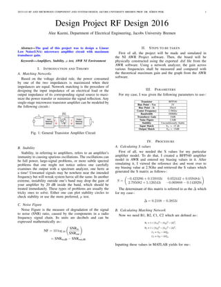
single-stage microwave transistor amplifier can be modeled by
the following circuit-:
Fig. 1: General Transistor Amplifier Circuit
B. Stability
Stability, in referring to amplifiers, refers to an amplifier’s
immunity to causing spurious oscillations. The oscillations can
be full power, large-signal problems, or more subtle spectral
problems that one might not notice unless one carefully
examines the output with a spectrum analyzer, one hertz at
a time! Unwanted signals may be nowhere near the intended
frequency but will wreak system havoc all the same. In another
extreme, instability outside one’s band may drop the gain of
your amplifier by 20 dB inside the band, which should be
treated immediately. These types of problems are usually the
tricky ones to solve. Either one can plot stability circles to
check stability or use the more preferred, µ test.
C. Noise Figure
Noise Figure is the measure of degradation of the signal
to noise (SNR) ratio, caused by the components in a radio
frequency signal chain. Its units are decibels and can be
expressed mathematically as-:
NF = 10 log 10
SNRin
SNRout
= SNRin,dB − SNRout,dB
II. STEPS TO BE TAKEN
First of all, the project will be made and simulated in
the NI AWR Project software. Then, the board will be
physically constructed using the exported .dxf file from the
AWR software. Using a network analyzer, the gain across
various frequencies shall be measured and compared with
the theoretical maximum gain and the graph from the AWR
software.
III. PARAMETERS
For my case, I was given the following parameters to use-:
Transistor BFP540
Bias Point - Vce 2V
Bias Point - Ic 20mA
Center Frequency 2.50Ghz
Bandwidth 100MHz
Transducer Gain 10dB
Noise Figure 2.5dB
Stability Unconditionally Stable
Input Match S11 = -15 db
Output Match S22 = -15dB
IV. PROCEDURE
A. Calculating S values
First of all, we needed the S values for my particular
amplifier model. To do that, I created a BFP540 amplifier
model in AWR and entered my biasing values in it. After
simulating it, I viewed the reference doc and went over to
my biasing value at 2.5Ghz and retrieved the S values which
generated the S matrix as follows-:
S =
−0.423286 + 0.159103i 0.052442 + 0.059484i
2.795082 + 5.126543i −0.069888 − 0.143929i
The determinant of this matrix is referred to as the ∆ which
for my case-:
∆ = 0.2108 − 0.3853i
B. Calculating Matching Network
Now we need B1, B2, C1, C2 which are defined as-:
Inputting these values in MATLAB yields for me-:
2. 20331143 RF AND MICROWAVE COMPONENT AND SYSTEM DESIGN, JACOBS UNIVERSITY BREMEN PROF. DR. S ¨OREN PEIK 2
B1 = 0.9860, B2=0.6282, C1 = -0.4640 + 0.1018i, C2
= 0.0807 - 0.2735i
Next we need to calculate the ΓS-:
and the ΓL-:
Inputting these into matlab yields two values for each but
choosing the smaller value gives us-:
ΓS = 0.7604λ, ΓL = 0.6395λ
Now we need to refer to the smith chart to get the
matching network lengths. The procedure is as follows. First
we find the absolute value and the phase of ΓS and the ΓL.
Next I mark the phase on the smith chart and measure the
length of the absolute value using the relative coefficient
marker. Now I plot these points on the smith chart. Next I
shift these points on the VSWR circle. Now I bring these
points down to the radial and subract from the original
phase and VSWR values to get the electrical lengths which I
multiply with 360 to get-:
C. Calculating Gain
Now we need to calculate the theoretical gain of the system
which is-:
When I input this into MATLAB, I get-:
GT = 16.3785
Now, I run the simulation in the AWR Environment. To
do so, I add a new graph and add the magnitude of every S
parameter into the graph against the frequency axis. After a
bit of fine tunings the axis values and parameters -:
My theoretical maximum gain is slightly below the maximum
gain from the graph for whose reason I could not figure out
but I suppose it has got to do with different capacitance
values.
D. Stability Test
Now we have to check for stability by performing a µ test
as follows-:
Inputting the values in matlab yields the following-:
µ = 1.3071
This is greater then 1 which means the system is
unconditionally stable and we do not need to plot stability
circles to test for stability.
We then performed a similar µ sweep test in the AWR
Environment.
3. 20331143 RF AND MICROWAVE COMPONENT AND SYSTEM DESIGN, JACOBS UNIVERSITY BREMEN PROF. DR. S ¨OREN PEIK 3
As we can see, the graph at the desired 2.5Ghz frequency has
a µ value higher then 1 which again proves that the system is
unconditionally stable. It should be noted that this amplifier is
not stable for frequencies roughly under 2.25Ghz since the µ
value drops below 1 there.
E. Shifting to Microstrip Design
Now, as mentioned in the instructions, the RO4003 substrate
was used from the Rogers Library which has a height of
32mil and thickness of 17µm.Next, we make use of the
TXline tool to translate these value on the RF level instead of
ideal lines. The width of the elements stays the same while
only the length changes as we get those values from the
TXline directly.
The next is the bias diagram-:
The Tuning and the TX-Line tool-:
(a) TX-Line
(b) Tuner
The Tuning tool was initally used to tune the value of the
resistor to just put the stability circle completely outside the
smith chart. After tuning it looked like this-:
I got an R value of 175ohm as shown in the previous
tuner screenshot. It should be noted that I also used the tuning
tool to closely match the maximum gain of the microstrip
circuit to that of the ideal circuit while making as minimalistic
changes as possible. The following were the S parameter
graph obtained when I plotted for the full fledge RF circuit-:
I tried my best but was no where able to cross the value of
13.71dB. Now I plot the µ stability graphs again. It can be
seen that the system is stable as both µ values are above 1.
A Noise performance, i.e. Noise figure over frequency using
MWO was also plotted for the new LNA circuit and is as
follows-:
4. 20331143 RF AND MICROWAVE COMPONENT AND SYSTEM DESIGN, JACOBS UNIVERSITY BREMEN PROF. DR. S ¨OREN PEIK 4
F. Microstrip Physical Design
The microstrip was finally compiled in AWR environment
and exported out using the .dxf format. Some minor changer
were later done by the professor to the diagram to accom-
modate physical space. Unfortunately, I dont have the new
schemetics with me and will be using my old submitted ones.
The diagram and physical figures are as follows. As one can
see they do not match for the aforementioned reason.
(a) The physical design that
was made. (b) The .dxf design
Fig. 3: Designs
G. Importing the graph from the Network Analyzer
The experiment was performed and the graph from the net-
work analyzer was imported into AWR. It looked as follows-:
As it can be seen, the theoretical maximum gain at 2.5 Ghz
is shown as 14.2dB which is quite close to what we got from
the AWR simulation. Moreover, plotting the stability µ plot
yields-:
The µ stability graph shows a value of 4.579 dB at 2.5Ghz
which is greater then 1 and shows that it is stable at that
particular center frequency.
V. CONCLUSION
The simulation that was made was quite close to the actual
physical parameters of the low noise amplifier. There were
slight variations of course but those were due to small factors
that we assumed to be ideal in the simulation. One of those
factors were the amount of solder used in soldering especially
when attaching the ports. We were also not required to plot
the stability circles because the µ test told us the result.
REFERENCES
[1] S. Peik, RF and Microwave Component and System design, Lecture Notes
2016
[2] D. Pozar, Microwave Engineering, 3rd edition 2015
[3] C. Bowick,Newnes, RF Circuit Design, 2nd edition 1997
[4] A. Matsuzawa RF circuit design: Basics, 1st edition