SlideShare a Scribd company logo
1 of 9
Download to read offline
International Journal of Engineering and Techniques - Volume 2 Issue 2, Mar – Apr 2016
ISSN: 2395-1303 http://www.ijetjournal.org Page 100
A Review on Single Stage Forward and Fly back Converter to
Improve its Performance
Gaurav B. Patil.1
, Paresh J. Shah.2
1(PG Scholar of Electrical Department, SSBT College, Jalgaon)
2 (Head of Electrical Department, SSBT College, Jalgaon)
I. INTRODUCTION
Recently power converters either AC-AC or DC-
DC are broadly used in a high and low Power
application. Traditionally, these AC-DC converters
are mostly consist of two stages. In the first stage,
AC voltage is converted into an uncontrolled DC
voltage using Diode and rectifiers, which gives its
output second stage of isolated DC-DC converters
as input using HF transformer for isolation. These
two-stage AC-DC converters have the problems of
power quality in terms of injected harmonic
currents at AC mains, caused voltage distortion,
degraded power factor, high crest factor, and large
size of DC capacitor filter at first stage. Though all
these concern are considered. Modern AC-DC
converters are being developed in single-stage to
improve power quality, reduced number of
components and high efficiency. These problems
can be avoided using newly developed single-stage
enhanced power quality AC-DC converters using
transformer isolation. They are also known as input
current shapers, high power-factor single-stage
converters, power factor correction (PFC)
converters; universal input single-stage PFC
isolated converters.
This paper deals with overview of enhanced
topologies of AC-DC converter with isolation. All
these enhanced single stage AC-DC converters with
isolation are generally classified.
Fig.1 Classification of AC-DC Converter
Fig. 1 shows the classification isolated single-phase
AC-DC converter. The enhanced power quality
AC-DC converters feed from single-phase AC
mains is classified into three major categories,
namely, buck, boost, and buck-boost topologies. All
these three types of converters are further classified
into four types of configurations. Some of these
converters are also known as single-phase, single-
stage converter or single-stage single-switch
converter).
Normally, fly back converter have good
power factor but having issues with high offset
current through the transformer magnetizing
Inductor, large core losses and low power
conversion efficiency. Whereas forward converter
can achieve good power conversion efficiency with
low core loss. They have low power factor. All
RESEARCH ARTICLE OPEN ACCESS
Abstract:
Universal demand for power increases due to continuous development to fulfil all these demand. Resources
are used with optimization. A high efficiency and high power factor converters are the major parts of energy
transfer system. This paper present a general review on single stage forward and flyback converter topologies to get
better its performance. This is paper presents a kind general idea of increasing efficiency and power factor of single
stage forward and fly back converter.
Keywords — Forward-Fly back, MOSFET, PFC, THD
International Journal of Engineering and Techniques - Volume 2 Issue 2, Mar – Apr 2016
ISSN: 2395-1303 http://www.ijetjournal.org Page 101
these limitations can be achieved by combining
both topologies in same package.
II. LITRATURE REVIEW
In this paper, a high efficiency and high power
factor single-stage balanced forward-flyback
converter merging a forward and fly back converter
topologies is studied. The conventional AC/DC fly
back converter can achieve a good power factor but
it has a high offset current through the transformer
magnetizing inductor, which results in a large core
loss and low power conversion efficiency. And, the
conventional forward converter can achieve the
good power conversion efficiency with the aid of
the low core loss but the input current dead zone
near zero cross AC input voltage deteriorates the
power factor. On the other hand, since the proposed
converter can operate as the forward and fly back
converters during switch on and off periods,
respectively, it cannot only perform the power
transfer during an entire switching period but also
achieve the high power factor due to the fly back
operation. Moreover, since the current balanced
capacitor can minimize the offset current through
the transformer magnetizing inductor regardless of
the AC input voltage, the core loss and volume of
the transformer can be minimized. Therefore, the
proposed converter features a high efficiency and
high power factor. To confirm the validity of the
proposed converter, theoretical analysis and
experimental results from a prototype of 24W LED
driver are presented. [1, 3]
Fly-back converters have been widely used
because of the irrelative simplicity and their
excellent performance for multi output applications.
They can save cost and volume compared with the
other converters, especially in moderate low power
applications. In a fly-back converter, a transformer
is adopted to achieve galvanic isolation and energy
storage. [2]
Global energy consumption tends to grow
continuously. To satisfy the demand for electric
power against a background of the depletion of
conventional, fossil resources the renewable energy
sources are becoming more popular. According to
the researches despite its fluctuating nature and
weather dependency the capacity of renewable
resources can satisfy overall universal demand for
power. High gain DC/DC converters are the key
part of renewable energy systems .The designing of
high gain DC/DC converters is compulsory by
severe demands. The power conditioning systems
for the photovoltaic power sources needs high step-
up voltage gain due to the low output of the
generating sources. A high step-up topology
employing a Series-connected Forward-Fly Back
converter, which has a series-connected output for
high boost voltage-transfer gain. Series-connected
Forward-Fly Back converter is a hybrid type of
forward and fly back converter. By stacking the
outputs of them extremely high voltage gain can be
obtained with small volume and high efficiency
with a galvanic isolation. The separated secondary
windings reduce the voltage stress of the secondary
rectifiers and results in high efficiency.[4]
In order to reduce output voltage ripple, it is
a common practice to place a large electrolytic
capacitor at the output of the conventional, single
phase capacitive rectifier. This results in power
converter with poor power factor and high total
harmonic distortion (THD). In recent years, many
high frequency power factor correction (PFC)
circuits and current shaping control techniques were
developed to meet certain standards. [5]
The Fly back converter can both step up and
step-down the input voltage, while maintaining the
same polarity and the same ground reference for the
input and output. MOSFETs are used as a switching
device in low power and high frequency switching
applications. It may be noted that, as the turn-on
and turn-off time of MOSFETs are lower as
compared to other switching devices, which reduces
the switching losses. High frequency operation of
MOSFET reduced size of filters components. These
converters are now being used for various
applications, such as Switched Mode Power Supply
(SMPS) etc. Due to designing and tuning of Fly
back converters it can be used to designing of an
optimized controller for isolated DC-DC Fly back
converter for constant voltage applications. [6]
The Zero Voltage Switching (ZVS)
technique is used to achieve soft switching. A
bidirectional boost converter is connected with an
output module as a Parallel Input Serial Output
configuration. The flyback converter with Voltage
Doubler Rectifier (VDR) acts as an output module.
International Journal of Engineering and Techniques - Volume 2 Issue 2, Mar – Apr 2016
ISSN: 2395-1303 http://www.ijetjournal.org Page 102
This connection makes a bidirectional boost
converter an active clamp circuit which is
connected to the output side in order to extend the
step up ratio. A converter with active clamp
technique is used to recycle the leakage energy, to
eliminate voltage spike due to coupled inductors
and also to provide a mechanism to achieve ZVS.
To overcome the efficiency degradation during
light load due to load dependent soft switching of
the ZVS, a control method using Pulse Width
Modulation (PWM) proportional to the load current
is used.[7]
A zero-voltage switching (ZVS) forward-
flyback DC-DC converter, which is able to process
and deliver power efficiently over a wide input
voltage variation. The converter operates at
boundary mode between current continuous and
discontinuous mode to achieve ZVS. Variable
frequency with fixed off time is used for reducing
core losses of the transformer, achieving high
efficiency.[10]
A new bridgeless buck PFC rectifier that
substantially improves efficiency at low line of the
universal line range is introduced. By eliminating
input bridge diodes, the proposed rectifier’s
efficiency is further improved. Moreover, the
rectifier doubles its output voltage, which extends
useable energy of the bulk capacitor after a drop-
out of the line voltage.[9]
III. CONCEPT OF FLY BACK CONVERTER
Fly-back converter is the most commonly used
SMPS circuit for low output power applications
where the output voltage needs to be isolated from
the input main supply. The output power of fly-
back type SMPS circuits may vary from few watts
to less than 100 watts. The overall circuit topology
of this converter is considerably simpler than other
SMPS circuits. Input to the circuit is generally
unregulated dc voltage obtained by rectifying the
utility ac voltage followed by a simple capacitor
filter. The circuit can offer single or multiple
isolated output voltages and can operate over wide
range of input voltage variation. In respect of
energy-efficiency, fly-back power supplies are
inferior to many other SMPS circuits but its simple
topology and low cost makes it popular in low
output power range. The commonly used fly-back
converter requires a single controllable switch like,
MOSFET and the usual switching frequency is in
the range of 100 kHz. A two-switch topology exists
that offers better energy efficiency and less voltage
stress across the switches but costs more and the
circuit complexity also increases slightly. The
present lesson is limited to the study of fly-back
circuit of single switch topology. Fig.2 shows the
basic topology of a fly-back circuit. Input to the
circuit may be unregulated dc voltage derived from
the utility ac supply after rectification and some
filtering. The ripple in dc voltage waveform is
generally of low frequency and the overall ripple
voltage waveform repeats at twice the ac mains
frequency.
Fig.2. Basic Topology of Fly-Back Converter.
Since the SMPS circuit is operated at much
higher frequency (in the range of 100 kHz) the
input voltage, in spite of being unregulated, may be
considered to have a constant magnitude during any
high frequency cycle. A fast switching device („S‟),
like a MOSFET, is used with fast dynamic control
over switch duty ratio (ratio of ON time to
switching time-period) to maintain the desired
output voltage. The transformer, in Fig.2, is used
for voltage isolation as well as for better matching
between input and output voltage and current
requirements.
IV. CONCEPT OF FORWARD CONVERTER
Forward converter is another popular switched
mode power supply (SMPS) circuit that is used for
producing isolated and controlled dc voltage from
the unregulated dc input supply. The forward
converter, when compared with the fly-back circuit,
International Journal of Engineering and Techniques - Volume 2 Issue 2, Mar – Apr 2016
ISSN: 2395-1303 http://www.ijetjournal.org Page 103
is generally more energy efficient and is used for
applications requiring little higher power output (in
the range of 100 watts to 200 watts). However the
circuit topology, especially the output filtering
circuit is not as simple as in the fly-back converter
Fig.3 shows the basic topology of the forward
converter. It consists of a fast switching device ‘S’
along with its control circuitry, a transformer with
its primary winding connected in series with switch
‘S’ to the input supply and a rectification and
filtering circuit for the transformer secondary
winding. The load is connected across the rectified
output of the transformer-secondary.
Fig.3. Basic forward converter topology
The transformer used in the forward converter is
to be an ideal transformer with no leakage fluxes,
zero magnetizing current and no losses. The basic
operation of the circuit is explained with different
mode operation here assuming ideal circuit
elements. In fact, due to the presence of finite
magnetizing current in a practical transformer,
tertiary winding needs to be introduced in the
transformer and the circuit topology changes
slightly.
V. SINGLE SWITCH CONVERTER
PFC circuit can be available in two forms, i.e.
single stage and two –stage scheme in two stage
schemes. In two stage scheme, AC-DC converter is
connected to the line to provide good input power
factor and generate regulated dc voltage. Generally
this voltage cannot directly supply the load since it
contains intolerable second harmonic content.
Therefore a ac/dc converter is cascade to tightly
regulate the output voltage. These two power stages
are controlled separately. And thus it makes
optimization of both converters possible. The main
drawbacks of this scheme are its higher cost and
larger size resulting from its increased component
number and complicated control circuits. The one –
stage PFC scheme combines the PFC circuit and the
voltage regulation circuit in one stage. Due to the
simplified power stage and control circuit of the
single stage scheme, it is attractive to many
applications with cost size.
Fig. 4. InputV-I characteristics of basic flyback converter
operating in DCM.
(a) Flyback converter in PFC application.
(b) Input current. (c) Input V-I characteristics.
Fig.5. Basic circuit schematic of proposed converter.
The isolated flyback converter circuit and its
input current waveform are shown in Fig. 4. (a) and
(b), respectively.[5] Since switching frequency, it is
reasonable to assume that the line voltage is
constant in a switching cycle.
The basic circuit schematic of proposed new
single stage single switch isolated converter is
shown in Fig.5.[5] The input circuit employs a
Flyback topology and the output circuit is a forward
converter. The power switch and storage capacitor
International Journal of Engineering and Techniques
ISSN: 2395-1303
are placed between the two circuits with diode D1
and D2 coordinating their two separate operations.
Table 1. Time intervals and staus of devices in
mode operation
Mode Time
interval
Conducting device
S D
1
D
2
D
3
M1 to<t<t1 × ×
M2 t1≤t≤t’2 × ×
t'2≤t≤t2 ×
M3 t2≤t≤to
+Ts
It can be shown that in steady state the converter
operates in three operation modes du
switching cycle. Table1. Shows three modes of
operations. According to corresponding times and
the status of the switching devices.
Fig.6. Theoretical key waveforms of proposed
converter.
Typical steady state operation waveforms are
shown in fig. 6. Which consist of three modes can
be deeply studied with table1 having output filter
maintains the output voltage until next switching
cycle begins. Considering all design parameters i.e.
maximum duty ratio, magnetizing inductance,
transform ratio, selection of capacitor, filter
inductance, power switch and diodes. The
waveforms of filtered line current, switch voltage
and current through diodes D1 were recorded at
International Journal of Engineering and Techniques - Volume 2 Issue 2, Mar –
http://www.ijetjournal.org
laced between the two circuits with diode D1
and D2 coordinating their two separate operations.
Table 1. Time intervals and staus of devices in
Conducting device
D
4
D
5
×
×
×
×
It can be shown that in steady state the converter
operates in three operation modes during one
three modes of
corresponding times and
. Theoretical key waveforms of proposed
on waveforms are
. Which consist of three modes can
be deeply studied with table1 having output filter
til next switching
cycle begins. Considering all design parameters i.e.
maximum duty ratio, magnetizing inductance,
transform ratio, selection of capacitor, filter
inductance, power switch and diodes. The
waveforms of filtered line current, switch voltage
and current through diodes D1 were recorded at
peak line voltage. It is found that simulated and
experimental waveforms are in a good agreement.
The line current waveforms are
and in phase with the line voltage, proving that
good power factor was achieved by this converter
topology. Fig.7. represents measu
and efficiency under different load condition.
(a) Input power factor
(b)Efficiency
Fig.7. Experimental efficiency and input power factor.
VI. Conventional single stage PFC converter
Recently, conventional single-
factor correction) LED drivers
which are well known as most cost
solutions. Fig.9. shows their transformer
magnetizing inductor currents. As shown in this
figure, the magnetizing inductor offset current of
fly back converter is larger than that of forward
– Apr 2016
Page 104
peak line voltage. It is found that simulated and
experimental waveforms are in a good agreement.
waveforms are almost sinusoidal
and in phase with the line voltage, proving that
ctor was achieved by this converter
asured power factor
and efficiency under different load condition.
(a) Input power factor
efficiency and input power factor.
Conventional single stage PFC converter
-stage PFC (power
factor correction) LED drivers shown in fig. 8,
which are well known as most cost effective
shows their transformer
magnetizing inductor currents. As shown in this
figure, the magnetizing inductor offset current of
fly back converter is larger than that of forward
International Journal of Engineering and Techniques - Volume 2 Issue 2, Mar – Apr 2016
ISSN: 2395-1303 http://www.ijetjournal.org Page 105
converter. The magnetizing inductor offset current
of fly back and forward converter is
< 	 	, >=
˳
( )
(1)
< 	 	, >= 1 + !
"#
$%&	
	'^2*+
(2)
(a) Single-stage flyback converter
(a) Single stage forward converter
Fig 8 Conventional single stage PFC converter circuits
Moreover, from equations (1) and (2), while the
magnetizing inductor offset current of flyback
converter is dependent on the load current Io, that
of forward converter is not. Therefore, as the load
current is more increased, the offset current of
flyback converter becomes larger, which might
result in the larger core loss and volume of
transformer. For these reasons, the forward
converter is superior to the flyback converter in
terms of the transformer size and energy conversion
efficiency.
Fig.9. Transformer magnetizing inductor currents of
conventional flyback and forward converters
Fig 10.PFC performance of forward and flyback
In the meanwhile, as shown in Fig. 10, while the
flyback converter can transfer the input energy to
the output side over an entire range of input
voltage, the forward converter cannot at the lower
input voltage than the reflected output voltage nVo
to the transformer primary side. This is because the
forward converter is originated from the step-down
buck topology. Therefore, the input current dead
zone near zero cross AC input voltage is always
observed and deteriorates the power factor in the
forward converter. Therefore, the flyback converter
is superior to the forward converter in terms of the
PFC performance.
International Journal of Engineering and Techniques - Volume 2 Issue 2, Mar – Apr 2016
ISSN: 2395-1303 http://www.ijetjournal.org Page 106
VII. Proposed single stage PFC forward flyback
converter
To solve all these problems, a high efficiency and
high power factor single-stage balanced forward-
flyback converter is proposed as shown in Fig.11.
Since the proposed converter merges the forward
and flyback topologies, it can operate as the
forward and flyback converters during switch turn-
on and off periods, respectively. Therefore, it
cannot only perform the power transfer during an
entire switching period but also achieve the high
power factor. Especially, since the charge balanced
capacitor Cb can make the proposed converter
perform the forward operation regardless of the
input voltage, the magnetizing inductor offset
current, core loss and transformer size can be
minimized.
Fig.11. Proposed single stage PFC forward flyback converter
circuit
Fig. 11 shows the circuit diagram of the proposed
forward flyback converter.[1] As shown in this
figure, its primary side is exactly same as that of the
conventional flyback converter consisting of one
power switch (M1) and one transformer. On the
other hand, its secondary side consists of one output
inductor (Lo) for forward operation, one DC
blocking capacitor (Cb) for balancing operation and
three output Diodes (D1, D2, D3). When M1 is
conducting, the proposed converter operates as a
forward converter. On the other hand, when M1 is
blocked, the proposed converter operates as a
flyback converter. However, if it is assumed that
the proposed converter has no balancing capacitor
Cb, abovementioned forward operation is possible
only when the reflected primary voltage Vin/n to
the transformer secondary side is higher than the
output voltage Vo. This is because the forward
converter is originated from the buck converter.
Therefore, the forward-flyback converter operates
only as a flyback converter over the range of Vin/n
< Vo. Especially, at the minimum input voltage
near Vin=90Vrms, Vin/n is lower than Vo during
most of periods and thus, the transformer has a
large magnetizing offset current similar to the
conventional flyback converter. In this case, the
transformer core loss and volume are also as large
as those of the conventional flyback converter. On
the other hand, if the balancing capacitor Cb is
serially inserted with the transformer secondary
side, it can make the average current through Cb
during forward operation become exactly same as
that during flyback operation by the charge balance
principle of Cb. In other words, since the voltage
across Cb charged by flyback operation is added to
the Vsec=Vin/n during forward operation,
Vin/n+Vcb becomes higher than Vo and thus, the
forward operation is possible even at Vin/n<Vo
(a) (b)
Fig.12. Primary and magnetizing currents of forward-flyback
converter according to the input voltage. (a) Without
balancing capacitor (b) with balancing capacitor
Therefore, the proposed forward-flyback converter
with the balancing capacitor Cb can always operate
as both forward and flyback converters regardless
of the input voltage.
Fig.12. shows the primary and magnetizing current
waveforms of the proposed converter operating in
the boundary conduction mode (BCM). And, Fig.12
(a) and (b) show current waveforms without and
with balancing capacitor Cb according to the input
voltage, respectively. As mentioned earlier, the
proposed converter with Cb can operate as both
forward and flyback converters over an entire range
of input voltage with the aid of Vcb. On the other
International Journal of Engineering and Techniques - Volume 2 Issue 2, Mar – Apr 2016
ISSN: 2395-1303 http://www.ijetjournal.org Page 107
hand, while the proposed converter without Cb can
transfer the input energy to the output side at
Vin/n>Vo, it cannot at Vin/n<Vo. As a result, the
proposed converter with balancing capacitor Cb
features a smaller magnetizing offset current,
resultant smaller core loss and more reduced
transformer volume.
Fig.13. Key waveforms of the proposed forward – flyback
converter
The circuit operation of the proposed converter is
basically divided into two modes according to the
conduction state of each switch as shown in fig.13.
first mode operation from time interval t0-t1 and
second from t1-t2. By considering all design
parameters regarding proposed converter its
performance is observed. Which also compared
with conventional proposed individual converters
and analysis conclude that it is suitable for low
power application. For experimental performance
of converter it’s operated with different root mean
square values of voltage and efficiency and power
factor is observed.
Fig.14. Comparisons of efficiency and power factor between
flyback and proposed forward-flyback converter
Fig. 14 shows the measured efficiency and power
factor of the proposed forward-flyback and
conventional flyback converters. As shown in this
figure, the proposed converter has the high power
factor above 95% over a wide range of input
voltage. Especially, its efficiency along wide input
voltage range is above 88.71% and higher than the
conventional converter by maximum 8.07% at
264Vrms. This high efficiency is due primarily to
the small transformer offset current and resultant
reduced core loss.
VIII. CONCLUSION
This paper discusses various topologies employed
for improvement of performance AC-DC converter.
Initially conventional forward flyback converter
uses two Transformers. This is having problems
regarding size and cost due to large number circuit
component. In order to overcome these drawbacks
of two stage scheme. One stage PFC scheme
adopted which combines fly back and forward
circuit in single stage it makes optimization of
converter in single package. Another issues of
magnetizing offset current , core loss are overcome
with single stage balanced forward –flyback type
proposed converter .which have current balanced
capacitor can minimize the offset current all the
way through the transformer magnetizing inductor
apart from input AC voltage and reduce core loss.
After this review we realized that single stage
International Journal of Engineering and Techniques - Volume 2 Issue 2, Mar – Apr 2016
ISSN: 2395-1303 http://www.ijetjournal.org Page 108
scheme is outstanding solution for low power
application. It also provides good power factor and
efficiency.
REFERENCES
[1] Yoon choi, Moon- Keum and Sang Kyoohan
,jeong-ilkang, “ High efficiency and High Power
Factor Single Stage Balanced Forward – Fly back
Converter”, Proceeding of the IEEE, pp. 822-827,
2013.
[2] Subhrajyoti Modak , Goutam Kumar Panda,
Pradip Kumar Saha and Sanskar Das , “Design of
Novel fly-back converter using PID controller”
Proceeding of IJAREEIE, Vol.4, pp. 289-297,Jan
2015.
[3] M. Venkatesh Kumar and K. Chandra, “Power
Factor Improvement using Single Stage Balanced
Forward Flyback Converter” Proceeding of IJIT,
Vol.3, No.4, pp. 640-645, July 2015.
[4] J. Lee, J. Park, H. Jeon, “Series-Connected
Forward–Flyback Converter for High Step-Up
Power Conversion,” IEEE Trans. Power
Electronics, Vol.26, No.12, pp.3629-3641, Dec.
2011.
[5] Hua-Min Xu, Xin-Bo Ruan, Yang-Guang Yan “
A Novel Forward Single-Stage Single-Switch
Power Factor Correction AC/DC converter”,
Proceeding of PESC, Vol.2, pp. 754-759, 2001.
[6] Abhinav Dogra, Kanchan pal, “Designing and
Tuning of PI Controller for Flyback Converter”,
Proceeding of IJETT, Vol. 13 No.3, Jul 2014.
[7] R. Sudha and P.M. Dhanasekaran, “DC—DC
Converter Using PID Controller and Pulse Width
Modulation Technique”, Proceeding of IJETT,
Vol.7, No.4, pp165-168, Jan 2014.
[8] Yonghan Kang, Byungcho Choi and Wonseok
Lim, "Analysis and Design of a Forward-Flyback
Converter Employing Two Transformers",
Proceeding of the IEEE, Vol. 1, pp. 357-362, June.
2001.
[9] Yungtaek Jang and Milan M. Jovanovic,
"Bridgeless Buck PFC Rectifier", Proceeding of the
APEC2010, pp. 23-29, Feb. 2010.
[10] F. Chen, E. Auadisian, J. Shen and I. Batarseh,
"Soft switching Forward-Flyback DC-DC
Converter", Proceeding of JECE, Vol.3, No.5, pp.
26-35, 2013.
[11] Sanjeevsingh and Bhimsingh,“ Comprehensive
study of single phase AC-DC power corrected
converter with High frequency isolation” ,IEEE
trans. On Industrial Informatics, Vol. 7, No. 4, pp.
540-556, Nov 2011.

More Related Content

What's hot

a switched capacitor bidirectional converter with high gain
a switched capacitor bidirectional converter with high gaina switched capacitor bidirectional converter with high gain
a switched capacitor bidirectional converter with high gainBIJU K.
 
Single-Phase Inverter with Energy Buffer and DC-DC Conversion Circuits
Single-Phase Inverter with Energy Buffer and DC-DC Conversion CircuitsSingle-Phase Inverter with Energy Buffer and DC-DC Conversion Circuits
Single-Phase Inverter with Energy Buffer and DC-DC Conversion CircuitsAsoka Technologies
 
IRJET- Implementation of Multilevel Inverter using Solar PV Array for Renewab...
IRJET- Implementation of Multilevel Inverter using Solar PV Array for Renewab...IRJET- Implementation of Multilevel Inverter using Solar PV Array for Renewab...
IRJET- Implementation of Multilevel Inverter using Solar PV Array for Renewab...IRJET Journal
 
Voltage Control of Dual Active Bridge Converter for CO-Amorphous Core Materia...
Voltage Control of Dual Active Bridge Converter for CO-Amorphous Core Materia...Voltage Control of Dual Active Bridge Converter for CO-Amorphous Core Materia...
Voltage Control of Dual Active Bridge Converter for CO-Amorphous Core Materia...kuldeep12555
 
An Asymmetrical Dc-Dc Converter with a High Voltage Gain
An Asymmetrical Dc-Dc Converter with a High Voltage GainAn Asymmetrical Dc-Dc Converter with a High Voltage Gain
An Asymmetrical Dc-Dc Converter with a High Voltage GainIJMER
 
Simulation and analysis of multilevel inverter with reduced number of switches
Simulation and analysis of multilevel inverter with reduced number of switchesSimulation and analysis of multilevel inverter with reduced number of switches
Simulation and analysis of multilevel inverter with reduced number of switchesIAEME Publication
 
Transformerless Buck-Boost Converter With Positive Output Voltage and Nominal...
Transformerless Buck-Boost Converter With Positive Output Voltage and Nominal...Transformerless Buck-Boost Converter With Positive Output Voltage and Nominal...
Transformerless Buck-Boost Converter With Positive Output Voltage and Nominal...paperpublications3
 
Stand alone regulated single phase five level inverter with coupled inductor
Stand alone regulated single phase five level inverter with coupled inductorStand alone regulated single phase five level inverter with coupled inductor
Stand alone regulated single phase five level inverter with coupled inductorIAEME Publication
 
A ZVS Interleaved Boost AC/DC Converter Using Super Capacitor Power for Hybri...
A ZVS Interleaved Boost AC/DC Converter Using Super Capacitor Power for Hybri...A ZVS Interleaved Boost AC/DC Converter Using Super Capacitor Power for Hybri...
A ZVS Interleaved Boost AC/DC Converter Using Super Capacitor Power for Hybri...IJMER
 
A review of pfc boost converters for hybrid electric vehicle battery chargers
A review of pfc boost converters for hybrid electric vehicle battery chargersA review of pfc boost converters for hybrid electric vehicle battery chargers
A review of pfc boost converters for hybrid electric vehicle battery chargersiaemedu
 
Analysis of Fuel Cell Based Multilevel DC-DC Boost Converter for Induction Motor
Analysis of Fuel Cell Based Multilevel DC-DC Boost Converter for Induction MotorAnalysis of Fuel Cell Based Multilevel DC-DC Boost Converter for Induction Motor
Analysis of Fuel Cell Based Multilevel DC-DC Boost Converter for Induction MotorIJMTST Journal
 
Half bridge converter with wide range zvs
Half bridge converter with wide range zvsHalf bridge converter with wide range zvs
Half bridge converter with wide range zvsIAEME Publication
 
Multilevel DC Link Inverter with Reduced Switches and Batteries
Multilevel DC Link Inverter with Reduced Switches and BatteriesMultilevel DC Link Inverter with Reduced Switches and Batteries
Multilevel DC Link Inverter with Reduced Switches and BatteriesIJPEDS-IAES
 
A novel single phase cascaded h-bridge inverter with new cell configuration a...
A novel single phase cascaded h-bridge inverter with new cell configuration a...A novel single phase cascaded h-bridge inverter with new cell configuration a...
A novel single phase cascaded h-bridge inverter with new cell configuration a...eSAT Publishing House
 

What's hot (20)

a switched capacitor bidirectional converter with high gain
a switched capacitor bidirectional converter with high gaina switched capacitor bidirectional converter with high gain
a switched capacitor bidirectional converter with high gain
 
Single-Phase Inverter with Energy Buffer and DC-DC Conversion Circuits
Single-Phase Inverter with Energy Buffer and DC-DC Conversion CircuitsSingle-Phase Inverter with Energy Buffer and DC-DC Conversion Circuits
Single-Phase Inverter with Energy Buffer and DC-DC Conversion Circuits
 
Bidirectional Resonant DC-DC converter for Microgrid Applications
Bidirectional Resonant DC-DC converter for Microgrid ApplicationsBidirectional Resonant DC-DC converter for Microgrid Applications
Bidirectional Resonant DC-DC converter for Microgrid Applications
 
Time response of FOPID controlled PV based cascaded landsman converter-invert...
Time response of FOPID controlled PV based cascaded landsman converter-invert...Time response of FOPID controlled PV based cascaded landsman converter-invert...
Time response of FOPID controlled PV based cascaded landsman converter-invert...
 
IRJET- Implementation of Multilevel Inverter using Solar PV Array for Renewab...
IRJET- Implementation of Multilevel Inverter using Solar PV Array for Renewab...IRJET- Implementation of Multilevel Inverter using Solar PV Array for Renewab...
IRJET- Implementation of Multilevel Inverter using Solar PV Array for Renewab...
 
Voltage Control of Dual Active Bridge Converter for CO-Amorphous Core Materia...
Voltage Control of Dual Active Bridge Converter for CO-Amorphous Core Materia...Voltage Control of Dual Active Bridge Converter for CO-Amorphous Core Materia...
Voltage Control of Dual Active Bridge Converter for CO-Amorphous Core Materia...
 
An Asymmetrical Dc-Dc Converter with a High Voltage Gain
An Asymmetrical Dc-Dc Converter with a High Voltage GainAn Asymmetrical Dc-Dc Converter with a High Voltage Gain
An Asymmetrical Dc-Dc Converter with a High Voltage Gain
 
Simulation and analysis of multilevel inverter with reduced number of switches
Simulation and analysis of multilevel inverter with reduced number of switchesSimulation and analysis of multilevel inverter with reduced number of switches
Simulation and analysis of multilevel inverter with reduced number of switches
 
High efficiency three phase nine level diode clamped multilevel inverter
High efficiency three phase nine level diode clamped multilevel inverterHigh efficiency three phase nine level diode clamped multilevel inverter
High efficiency three phase nine level diode clamped multilevel inverter
 
Transformerless Buck-Boost Converter With Positive Output Voltage and Nominal...
Transformerless Buck-Boost Converter With Positive Output Voltage and Nominal...Transformerless Buck-Boost Converter With Positive Output Voltage and Nominal...
Transformerless Buck-Boost Converter With Positive Output Voltage and Nominal...
 
M43067982
M43067982M43067982
M43067982
 
Stand alone regulated single phase five level inverter with coupled inductor
Stand alone regulated single phase five level inverter with coupled inductorStand alone regulated single phase five level inverter with coupled inductor
Stand alone regulated single phase five level inverter with coupled inductor
 
A ZVS Interleaved Boost AC/DC Converter Using Super Capacitor Power for Hybri...
A ZVS Interleaved Boost AC/DC Converter Using Super Capacitor Power for Hybri...A ZVS Interleaved Boost AC/DC Converter Using Super Capacitor Power for Hybri...
A ZVS Interleaved Boost AC/DC Converter Using Super Capacitor Power for Hybri...
 
A review of pfc boost converters for hybrid electric vehicle battery chargers
A review of pfc boost converters for hybrid electric vehicle battery chargersA review of pfc boost converters for hybrid electric vehicle battery chargers
A review of pfc boost converters for hybrid electric vehicle battery chargers
 
Analysis of Fuel Cell Based Multilevel DC-DC Boost Converter for Induction Motor
Analysis of Fuel Cell Based Multilevel DC-DC Boost Converter for Induction MotorAnalysis of Fuel Cell Based Multilevel DC-DC Boost Converter for Induction Motor
Analysis of Fuel Cell Based Multilevel DC-DC Boost Converter for Induction Motor
 
Half bridge converter with wide range zvs
Half bridge converter with wide range zvsHalf bridge converter with wide range zvs
Half bridge converter with wide range zvs
 
Multilevel DC Link Inverter with Reduced Switches and Batteries
Multilevel DC Link Inverter with Reduced Switches and BatteriesMultilevel DC Link Inverter with Reduced Switches and Batteries
Multilevel DC Link Inverter with Reduced Switches and Batteries
 
Lg3619211926
Lg3619211926Lg3619211926
Lg3619211926
 
A novel single phase cascaded h-bridge inverter with new cell configuration a...
A novel single phase cascaded h-bridge inverter with new cell configuration a...A novel single phase cascaded h-bridge inverter with new cell configuration a...
A novel single phase cascaded h-bridge inverter with new cell configuration a...
 
Current mode proportional resonant controlled multi input–SEPIC-re-boost-system
Current mode proportional resonant controlled multi input–SEPIC-re-boost-systemCurrent mode proportional resonant controlled multi input–SEPIC-re-boost-system
Current mode proportional resonant controlled multi input–SEPIC-re-boost-system
 

Viewers also liked

Viewers also liked (19)

[IJET V2I4P4] Authors: Miss. Smita .A. Bhole
[IJET V2I4P4] Authors: Miss. Smita .A. Bhole[IJET V2I4P4] Authors: Miss. Smita .A. Bhole
[IJET V2I4P4] Authors: Miss. Smita .A. Bhole
 
[IJET V2I2P29] Authors: Praveen Ghuge, ChavanNitishR. ,KatteSagar S. ,PawarSu...
[IJET V2I2P29] Authors: Praveen Ghuge, ChavanNitishR. ,KatteSagar S. ,PawarSu...[IJET V2I2P29] Authors: Praveen Ghuge, ChavanNitishR. ,KatteSagar S. ,PawarSu...
[IJET V2I2P29] Authors: Praveen Ghuge, ChavanNitishR. ,KatteSagar S. ,PawarSu...
 
[IJCT-V3I2P17] Authors: Sheng Lai, Xiaohua Meng, Dongqin Zheng
[IJCT-V3I2P17] Authors: Sheng Lai, Xiaohua Meng, Dongqin Zheng[IJCT-V3I2P17] Authors: Sheng Lai, Xiaohua Meng, Dongqin Zheng
[IJCT-V3I2P17] Authors: Sheng Lai, Xiaohua Meng, Dongqin Zheng
 
[IJET V2I3-1P3] Authors:G.Siva Prasad K.Dinesh Achari E.Dileep Kumar Goud M.N...
[IJET V2I3-1P3] Authors:G.Siva Prasad K.Dinesh Achari E.Dileep Kumar Goud M.N...[IJET V2I3-1P3] Authors:G.Siva Prasad K.Dinesh Achari E.Dileep Kumar Goud M.N...
[IJET V2I3-1P3] Authors:G.Siva Prasad K.Dinesh Achari E.Dileep Kumar Goud M.N...
 
[IJET V2I3P11] Authors: Payal More, Rohini Pandit, Supriya Makude, Harsh Nirb...
[IJET V2I3P11] Authors: Payal More, Rohini Pandit, Supriya Makude, Harsh Nirb...[IJET V2I3P11] Authors: Payal More, Rohini Pandit, Supriya Makude, Harsh Nirb...
[IJET V2I3P11] Authors: Payal More, Rohini Pandit, Supriya Makude, Harsh Nirb...
 
[IJET-V1I2P1] Authors :Imran Ullah Khan ,Mohd. Javed Khan ,S.Hasan Saeed ,Nup...
[IJET-V1I2P1] Authors :Imran Ullah Khan ,Mohd. Javed Khan ,S.Hasan Saeed ,Nup...[IJET-V1I2P1] Authors :Imran Ullah Khan ,Mohd. Javed Khan ,S.Hasan Saeed ,Nup...
[IJET-V1I2P1] Authors :Imran Ullah Khan ,Mohd. Javed Khan ,S.Hasan Saeed ,Nup...
 
[IJET V2I3P15] Authors: Sidharam Ambadas Basargi, Prof Gopal Joshi
[IJET V2I3P15] Authors: Sidharam Ambadas Basargi, Prof Gopal Joshi[IJET V2I3P15] Authors: Sidharam Ambadas Basargi, Prof Gopal Joshi
[IJET V2I3P15] Authors: Sidharam Ambadas Basargi, Prof Gopal Joshi
 
[IJET - V1I1P1] Author :Husssain Babu, Mohammad Ali
[IJET - V1I1P1] Author :Husssain Babu, Mohammad Ali [IJET - V1I1P1] Author :Husssain Babu, Mohammad Ali
[IJET - V1I1P1] Author :Husssain Babu, Mohammad Ali
 
[IJET V2I2P28] Authors: ROSA MAHTOUT, FARID ZAIDI, LINDA OULD SAADI, SOUHILA ...
[IJET V2I2P28] Authors: ROSA MAHTOUT, FARID ZAIDI, LINDA OULD SAADI, SOUHILA ...[IJET V2I2P28] Authors: ROSA MAHTOUT, FARID ZAIDI, LINDA OULD SAADI, SOUHILA ...
[IJET V2I2P28] Authors: ROSA MAHTOUT, FARID ZAIDI, LINDA OULD SAADI, SOUHILA ...
 
[IJCT-V3I2P24] Authors: Osama H. Abdelwahed; and M. El-Sayed Wahed
[IJCT-V3I2P24] Authors: Osama H. Abdelwahed; and M. El-Sayed Wahed[IJCT-V3I2P24] Authors: Osama H. Abdelwahed; and M. El-Sayed Wahed
[IJCT-V3I2P24] Authors: Osama H. Abdelwahed; and M. El-Sayed Wahed
 
[IJET V2I3P13] Authors: Anshika, Sujit Tak, Sandeep Ugale, Abhishek Pohekar
[IJET V2I3P13] Authors: Anshika, Sujit Tak, Sandeep Ugale, Abhishek Pohekar[IJET V2I3P13] Authors: Anshika, Sujit Tak, Sandeep Ugale, Abhishek Pohekar
[IJET V2I3P13] Authors: Anshika, Sujit Tak, Sandeep Ugale, Abhishek Pohekar
 
[IJCT-V3I2P26] Authors: Sunny Sharma
[IJCT-V3I2P26] Authors: Sunny Sharma[IJCT-V3I2P26] Authors: Sunny Sharma
[IJCT-V3I2P26] Authors: Sunny Sharma
 
[IJET V2I3P2] Authors: Shraddha Kallappa Walikar, Dr. Aswatha Kumar M
[IJET V2I3P2] Authors: Shraddha Kallappa Walikar,  Dr. Aswatha Kumar M[IJET V2I3P2] Authors: Shraddha Kallappa Walikar,  Dr. Aswatha Kumar M
[IJET V2I3P2] Authors: Shraddha Kallappa Walikar, Dr. Aswatha Kumar M
 
[IJCT-V3I2P23] Authors: Baljinder Kaur, Narinder Sharma
[IJCT-V3I2P23] Authors: Baljinder Kaur, Narinder Sharma[IJCT-V3I2P23] Authors: Baljinder Kaur, Narinder Sharma
[IJCT-V3I2P23] Authors: Baljinder Kaur, Narinder Sharma
 
[IJET V2I2P23] Authors: K. Deepika, Sudha M. S., Sandhya Rani M.H
[IJET V2I2P23] Authors: K. Deepika, Sudha M. S., Sandhya Rani M.H[IJET V2I2P23] Authors: K. Deepika, Sudha M. S., Sandhya Rani M.H
[IJET V2I2P23] Authors: K. Deepika, Sudha M. S., Sandhya Rani M.H
 
[IJET-V1I2P4] Authors :Mrs.Rita S. Pimpalkar, Rutuja U. Joshi, Rakesh R. Khan...
[IJET-V1I2P4] Authors :Mrs.Rita S. Pimpalkar, Rutuja U. Joshi, Rakesh R. Khan...[IJET-V1I2P4] Authors :Mrs.Rita S. Pimpalkar, Rutuja U. Joshi, Rakesh R. Khan...
[IJET-V1I2P4] Authors :Mrs.Rita S. Pimpalkar, Rutuja U. Joshi, Rakesh R. Khan...
 
[IJET-V2I3P18] Authors: Mr. B. N. Patil , Mr. Sandesh Sonar , Mr. Pavankumar ...
[IJET-V2I3P18] Authors: Mr. B. N. Patil , Mr. Sandesh Sonar , Mr. Pavankumar ...[IJET-V2I3P18] Authors: Mr. B. N. Patil , Mr. Sandesh Sonar , Mr. Pavankumar ...
[IJET-V2I3P18] Authors: Mr. B. N. Patil , Mr. Sandesh Sonar , Mr. Pavankumar ...
 
[IJET V2I2P24] Authors: Galal Ali Hassaan
[IJET V2I2P24] Authors: Galal Ali Hassaan[IJET V2I2P24] Authors: Galal Ali Hassaan
[IJET V2I2P24] Authors: Galal Ali Hassaan
 
[IJET-V2I3P17] Authors: R.C.Rohini, G.Srividhya
[IJET-V2I3P17] Authors: R.C.Rohini, G.Srividhya[IJET-V2I3P17] Authors: R.C.Rohini, G.Srividhya
[IJET-V2I3P17] Authors: R.C.Rohini, G.Srividhya
 

Similar to [IJET- V2I2P17] Authors: Gaurav B. Patil., Paresh J. Shah

A high efficiency step up current-fed
A high efficiency step up current-fedA high efficiency step up current-fed
A high efficiency step up current-fednexgentechnology
 
High-Power Bidirectional Dual Active Bridge and Double Dual Active Bridge DC-...
High-Power Bidirectional Dual Active Bridge and Double Dual Active Bridge DC-...High-Power Bidirectional Dual Active Bridge and Double Dual Active Bridge DC-...
High-Power Bidirectional Dual Active Bridge and Double Dual Active Bridge DC-...IRJET Journal
 
About SOLID STATE TRANSFORMER
About SOLID STATE TRANSFORMERAbout SOLID STATE TRANSFORMER
About SOLID STATE TRANSFORMERBalaNaik2
 
Design of an Integrated Power Factor Converter with PI Controller for Low Pow...
Design of an Integrated Power Factor Converter with PI Controller for Low Pow...Design of an Integrated Power Factor Converter with PI Controller for Low Pow...
Design of an Integrated Power Factor Converter with PI Controller for Low Pow...IOSRJEEE
 
Novel High Voltage Buck Boost Converter
Novel High Voltage Buck Boost ConverterNovel High Voltage Buck Boost Converter
Novel High Voltage Buck Boost ConverterIRJET Journal
 
A Five – Level Integrated AC – DC Converter
A Five – Level Integrated AC – DC ConverterA Five – Level Integrated AC – DC Converter
A Five – Level Integrated AC – DC ConverterIJTET Journal
 
International Refereed Journal of Engineering and Science (IRJES)
International Refereed Journal of Engineering and Science (IRJES)International Refereed Journal of Engineering and Science (IRJES)
International Refereed Journal of Engineering and Science (IRJES)irjes
 
IRJET- High Efficiency Bridge-Less Battery Charger for Light Electric Veh...
IRJET-  	  High Efficiency Bridge-Less Battery Charger for Light Electric Veh...IRJET-  	  High Efficiency Bridge-Less Battery Charger for Light Electric Veh...
IRJET- High Efficiency Bridge-Less Battery Charger for Light Electric Veh...IRJET Journal
 
Design and implementation of Closed Loop Control of Three Phase Interleaved P...
Design and implementation of Closed Loop Control of Three Phase Interleaved P...Design and implementation of Closed Loop Control of Three Phase Interleaved P...
Design and implementation of Closed Loop Control of Three Phase Interleaved P...IJMTST Journal
 
A Novel Integrated AC-DC Five Level Converter Strategy for Power Factor Corre...
A Novel Integrated AC-DC Five Level Converter Strategy for Power Factor Corre...A Novel Integrated AC-DC Five Level Converter Strategy for Power Factor Corre...
A Novel Integrated AC-DC Five Level Converter Strategy for Power Factor Corre...IJMTST Journal
 
IRJET- A Systematic Approach to Design Single Phase Transformer Less Inve...
IRJET-  	  A Systematic Approach to Design Single Phase Transformer Less Inve...IRJET-  	  A Systematic Approach to Design Single Phase Transformer Less Inve...
IRJET- A Systematic Approach to Design Single Phase Transformer Less Inve...IRJET Journal
 
Presentation on DC-DC converter for EV
Presentation on DC-DC converter for EVPresentation on DC-DC converter for EV
Presentation on DC-DC converter for EVUdayaKumar120822
 
IRJET- 127 Multilevel Inverter
IRJET- 127 Multilevel InverterIRJET- 127 Multilevel Inverter
IRJET- 127 Multilevel InverterIRJET Journal
 
PV Cell Fed High Step-up DC-DC Converter for PMSM Drive Applications
PV Cell Fed High Step-up DC-DC Converter for PMSM Drive ApplicationsPV Cell Fed High Step-up DC-DC Converter for PMSM Drive Applications
PV Cell Fed High Step-up DC-DC Converter for PMSM Drive ApplicationsIJMTST Journal
 
Research Inventy : International Journal of Engineering and Science
Research Inventy : International Journal of Engineering and ScienceResearch Inventy : International Journal of Engineering and Science
Research Inventy : International Journal of Engineering and Scienceresearchinventy
 
Power Quality Analysis Using Active NPC Multilevel inverter in PV sourced sta...
Power Quality Analysis Using Active NPC Multilevel inverter in PV sourced sta...Power Quality Analysis Using Active NPC Multilevel inverter in PV sourced sta...
Power Quality Analysis Using Active NPC Multilevel inverter in PV sourced sta...IRJET Journal
 
Defination of dc to dc conv
Defination of dc to dc convDefination of dc to dc conv
Defination of dc to dc convravikant_019
 

Similar to [IJET- V2I2P17] Authors: Gaurav B. Patil., Paresh J. Shah (20)

A high efficiency step up current-fed
A high efficiency step up current-fedA high efficiency step up current-fed
A high efficiency step up current-fed
 
High-Power Bidirectional Dual Active Bridge and Double Dual Active Bridge DC-...
High-Power Bidirectional Dual Active Bridge and Double Dual Active Bridge DC-...High-Power Bidirectional Dual Active Bridge and Double Dual Active Bridge DC-...
High-Power Bidirectional Dual Active Bridge and Double Dual Active Bridge DC-...
 
About SOLID STATE TRANSFORMER
About SOLID STATE TRANSFORMERAbout SOLID STATE TRANSFORMER
About SOLID STATE TRANSFORMER
 
Design of an Integrated Power Factor Converter with PI Controller for Low Pow...
Design of an Integrated Power Factor Converter with PI Controller for Low Pow...Design of an Integrated Power Factor Converter with PI Controller for Low Pow...
Design of an Integrated Power Factor Converter with PI Controller for Low Pow...
 
Novel High Voltage Buck Boost Converter
Novel High Voltage Buck Boost ConverterNovel High Voltage Buck Boost Converter
Novel High Voltage Buck Boost Converter
 
A Five – Level Integrated AC – DC Converter
A Five – Level Integrated AC – DC ConverterA Five – Level Integrated AC – DC Converter
A Five – Level Integrated AC – DC Converter
 
International Refereed Journal of Engineering and Science (IRJES)
International Refereed Journal of Engineering and Science (IRJES)International Refereed Journal of Engineering and Science (IRJES)
International Refereed Journal of Engineering and Science (IRJES)
 
IRJET- High Efficiency Bridge-Less Battery Charger for Light Electric Veh...
IRJET-  	  High Efficiency Bridge-Less Battery Charger for Light Electric Veh...IRJET-  	  High Efficiency Bridge-Less Battery Charger for Light Electric Veh...
IRJET- High Efficiency Bridge-Less Battery Charger for Light Electric Veh...
 
Design and implementation of Closed Loop Control of Three Phase Interleaved P...
Design and implementation of Closed Loop Control of Three Phase Interleaved P...Design and implementation of Closed Loop Control of Three Phase Interleaved P...
Design and implementation of Closed Loop Control of Three Phase Interleaved P...
 
A Novel Integrated AC-DC Five Level Converter Strategy for Power Factor Corre...
A Novel Integrated AC-DC Five Level Converter Strategy for Power Factor Corre...A Novel Integrated AC-DC Five Level Converter Strategy for Power Factor Corre...
A Novel Integrated AC-DC Five Level Converter Strategy for Power Factor Corre...
 
IRJET- A Systematic Approach to Design Single Phase Transformer Less Inve...
IRJET-  	  A Systematic Approach to Design Single Phase Transformer Less Inve...IRJET-  	  A Systematic Approach to Design Single Phase Transformer Less Inve...
IRJET- A Systematic Approach to Design Single Phase Transformer Less Inve...
 
Presentation on DC-DC converter for EV
Presentation on DC-DC converter for EVPresentation on DC-DC converter for EV
Presentation on DC-DC converter for EV
 
IRJET- 127 Multilevel Inverter
IRJET- 127 Multilevel InverterIRJET- 127 Multilevel Inverter
IRJET- 127 Multilevel Inverter
 
Simulation and Analysis of Multiphase Boost Converter with Soft-Switching for...
Simulation and Analysis of Multiphase Boost Converter with Soft-Switching for...Simulation and Analysis of Multiphase Boost Converter with Soft-Switching for...
Simulation and Analysis of Multiphase Boost Converter with Soft-Switching for...
 
PV Cell Fed High Step-up DC-DC Converter for PMSM Drive Applications
PV Cell Fed High Step-up DC-DC Converter for PMSM Drive ApplicationsPV Cell Fed High Step-up DC-DC Converter for PMSM Drive Applications
PV Cell Fed High Step-up DC-DC Converter for PMSM Drive Applications
 
Research Inventy : International Journal of Engineering and Science
Research Inventy : International Journal of Engineering and ScienceResearch Inventy : International Journal of Engineering and Science
Research Inventy : International Journal of Engineering and Science
 
Modeling of single phase off-grid inverter for small standalone system applic...
Modeling of single phase off-grid inverter for small standalone system applic...Modeling of single phase off-grid inverter for small standalone system applic...
Modeling of single phase off-grid inverter for small standalone system applic...
 
Power Quality Analysis Using Active NPC Multilevel inverter in PV sourced sta...
Power Quality Analysis Using Active NPC Multilevel inverter in PV sourced sta...Power Quality Analysis Using Active NPC Multilevel inverter in PV sourced sta...
Power Quality Analysis Using Active NPC Multilevel inverter in PV sourced sta...
 
Power Quality Analysis Using Active NPC Multilevel inverter in PV sourced sta...
Power Quality Analysis Using Active NPC Multilevel inverter in PV sourced sta...Power Quality Analysis Using Active NPC Multilevel inverter in PV sourced sta...
Power Quality Analysis Using Active NPC Multilevel inverter in PV sourced sta...
 
Defination of dc to dc conv
Defination of dc to dc convDefination of dc to dc conv
Defination of dc to dc conv
 

More from IJET - International Journal of Engineering and Techniques

More from IJET - International Journal of Engineering and Techniques (20)

healthcare supervising system to monitor heart rate to diagonize and alert he...
healthcare supervising system to monitor heart rate to diagonize and alert he...healthcare supervising system to monitor heart rate to diagonize and alert he...
healthcare supervising system to monitor heart rate to diagonize and alert he...
 
verifiable and multi-keyword searchable attribute-based encryption scheme for...
verifiable and multi-keyword searchable attribute-based encryption scheme for...verifiable and multi-keyword searchable attribute-based encryption scheme for...
verifiable and multi-keyword searchable attribute-based encryption scheme for...
 
Ijet v5 i6p18
Ijet v5 i6p18Ijet v5 i6p18
Ijet v5 i6p18
 
Ijet v5 i6p17
Ijet v5 i6p17Ijet v5 i6p17
Ijet v5 i6p17
 
Ijet v5 i6p16
Ijet v5 i6p16Ijet v5 i6p16
Ijet v5 i6p16
 
Ijet v5 i6p15
Ijet v5 i6p15Ijet v5 i6p15
Ijet v5 i6p15
 
Ijet v5 i6p14
Ijet v5 i6p14Ijet v5 i6p14
Ijet v5 i6p14
 
Ijet v5 i6p13
Ijet v5 i6p13Ijet v5 i6p13
Ijet v5 i6p13
 
Ijet v5 i6p12
Ijet v5 i6p12Ijet v5 i6p12
Ijet v5 i6p12
 
Ijet v5 i6p11
Ijet v5 i6p11Ijet v5 i6p11
Ijet v5 i6p11
 
Ijet v5 i6p10
Ijet v5 i6p10Ijet v5 i6p10
Ijet v5 i6p10
 
Ijet v5 i6p2
Ijet v5 i6p2Ijet v5 i6p2
Ijet v5 i6p2
 
IJET-V3I2P24
IJET-V3I2P24IJET-V3I2P24
IJET-V3I2P24
 
IJET-V3I2P23
IJET-V3I2P23IJET-V3I2P23
IJET-V3I2P23
 
IJET-V3I2P22
IJET-V3I2P22IJET-V3I2P22
IJET-V3I2P22
 
IJET-V3I2P21
IJET-V3I2P21IJET-V3I2P21
IJET-V3I2P21
 
IJET-V3I2P20
IJET-V3I2P20IJET-V3I2P20
IJET-V3I2P20
 
IJET-V3I2P19
IJET-V3I2P19IJET-V3I2P19
IJET-V3I2P19
 
IJET-V3I2P18
IJET-V3I2P18IJET-V3I2P18
IJET-V3I2P18
 
IJET-V3I2P17
IJET-V3I2P17IJET-V3I2P17
IJET-V3I2P17
 

Recently uploaded

Gurgaon ✡️9711147426✨Call In girls Gurgaon Sector 51 escort service
Gurgaon ✡️9711147426✨Call In girls Gurgaon Sector 51 escort serviceGurgaon ✡️9711147426✨Call In girls Gurgaon Sector 51 escort service
Gurgaon ✡️9711147426✨Call In girls Gurgaon Sector 51 escort servicejennyeacort
 
Past, Present and Future of Generative AI
Past, Present and Future of Generative AIPast, Present and Future of Generative AI
Past, Present and Future of Generative AIabhishek36461
 
Study on Air-Water & Water-Water Heat Exchange in a Finned Tube Exchanger
Study on Air-Water & Water-Water Heat Exchange in a Finned Tube ExchangerStudy on Air-Water & Water-Water Heat Exchange in a Finned Tube Exchanger
Study on Air-Water & Water-Water Heat Exchange in a Finned Tube ExchangerAnamika Sarkar
 
Arduino_CSE ece ppt for working and principal of arduino.ppt
Arduino_CSE ece ppt for working and principal of arduino.pptArduino_CSE ece ppt for working and principal of arduino.ppt
Arduino_CSE ece ppt for working and principal of arduino.pptSAURABHKUMAR892774
 
Software and Systems Engineering Standards: Verification and Validation of Sy...
Software and Systems Engineering Standards: Verification and Validation of Sy...Software and Systems Engineering Standards: Verification and Validation of Sy...
Software and Systems Engineering Standards: Verification and Validation of Sy...VICTOR MAESTRE RAMIREZ
 
INFLUENCE OF NANOSILICA ON THE PROPERTIES OF CONCRETE
INFLUENCE OF NANOSILICA ON THE PROPERTIES OF CONCRETEINFLUENCE OF NANOSILICA ON THE PROPERTIES OF CONCRETE
INFLUENCE OF NANOSILICA ON THE PROPERTIES OF CONCRETEroselinkalist12
 
Why does (not) Kafka need fsync: Eliminating tail latency spikes caused by fsync
Why does (not) Kafka need fsync: Eliminating tail latency spikes caused by fsyncWhy does (not) Kafka need fsync: Eliminating tail latency spikes caused by fsync
Why does (not) Kafka need fsync: Eliminating tail latency spikes caused by fsyncssuser2ae721
 
Introduction-To-Agricultural-Surveillance-Rover.pptx
Introduction-To-Agricultural-Surveillance-Rover.pptxIntroduction-To-Agricultural-Surveillance-Rover.pptx
Introduction-To-Agricultural-Surveillance-Rover.pptxk795866
 
CCS355 Neural Network & Deep Learning UNIT III notes and Question bank .pdf
CCS355 Neural Network & Deep Learning UNIT III notes and Question bank .pdfCCS355 Neural Network & Deep Learning UNIT III notes and Question bank .pdf
CCS355 Neural Network & Deep Learning UNIT III notes and Question bank .pdfAsst.prof M.Gokilavani
 
IVE Industry Focused Event - Defence Sector 2024
IVE Industry Focused Event - Defence Sector 2024IVE Industry Focused Event - Defence Sector 2024
IVE Industry Focused Event - Defence Sector 2024Mark Billinghurst
 
Vishratwadi & Ghorpadi Bridge Tender documents
Vishratwadi & Ghorpadi Bridge Tender documentsVishratwadi & Ghorpadi Bridge Tender documents
Vishratwadi & Ghorpadi Bridge Tender documentsSachinPawar510423
 
Oxy acetylene welding presentation note.
Oxy acetylene welding presentation note.Oxy acetylene welding presentation note.
Oxy acetylene welding presentation note.eptoze12
 
Risk Assessment For Installation of Drainage Pipes.pdf
Risk Assessment For Installation of Drainage Pipes.pdfRisk Assessment For Installation of Drainage Pipes.pdf
Risk Assessment For Installation of Drainage Pipes.pdfROCENODodongVILLACER
 
Concrete Mix Design - IS 10262-2019 - .pptx
Concrete Mix Design - IS 10262-2019 - .pptxConcrete Mix Design - IS 10262-2019 - .pptx
Concrete Mix Design - IS 10262-2019 - .pptxKartikeyaDwivedi3
 
Solving The Right Triangles PowerPoint 2.ppt
Solving The Right Triangles PowerPoint 2.pptSolving The Right Triangles PowerPoint 2.ppt
Solving The Right Triangles PowerPoint 2.pptJasonTagapanGulla
 
Indian Dairy Industry Present Status and.ppt
Indian Dairy Industry Present Status and.pptIndian Dairy Industry Present Status and.ppt
Indian Dairy Industry Present Status and.pptMadan Karki
 
Introduction to Machine Learning Unit-3 for II MECH
Introduction to Machine Learning Unit-3 for II MECHIntroduction to Machine Learning Unit-3 for II MECH
Introduction to Machine Learning Unit-3 for II MECHC Sai Kiran
 
Work Experience-Dalton Park.pptxfvvvvvvv
Work Experience-Dalton Park.pptxfvvvvvvvWork Experience-Dalton Park.pptxfvvvvvvv
Work Experience-Dalton Park.pptxfvvvvvvvLewisJB
 

Recently uploaded (20)

Gurgaon ✡️9711147426✨Call In girls Gurgaon Sector 51 escort service
Gurgaon ✡️9711147426✨Call In girls Gurgaon Sector 51 escort serviceGurgaon ✡️9711147426✨Call In girls Gurgaon Sector 51 escort service
Gurgaon ✡️9711147426✨Call In girls Gurgaon Sector 51 escort service
 
Past, Present and Future of Generative AI
Past, Present and Future of Generative AIPast, Present and Future of Generative AI
Past, Present and Future of Generative AI
 
Study on Air-Water & Water-Water Heat Exchange in a Finned Tube Exchanger
Study on Air-Water & Water-Water Heat Exchange in a Finned Tube ExchangerStudy on Air-Water & Water-Water Heat Exchange in a Finned Tube Exchanger
Study on Air-Water & Water-Water Heat Exchange in a Finned Tube Exchanger
 
Arduino_CSE ece ppt for working and principal of arduino.ppt
Arduino_CSE ece ppt for working and principal of arduino.pptArduino_CSE ece ppt for working and principal of arduino.ppt
Arduino_CSE ece ppt for working and principal of arduino.ppt
 
Software and Systems Engineering Standards: Verification and Validation of Sy...
Software and Systems Engineering Standards: Verification and Validation of Sy...Software and Systems Engineering Standards: Verification and Validation of Sy...
Software and Systems Engineering Standards: Verification and Validation of Sy...
 
🔝9953056974🔝!!-YOUNG call girls in Rajendra Nagar Escort rvice Shot 2000 nigh...
🔝9953056974🔝!!-YOUNG call girls in Rajendra Nagar Escort rvice Shot 2000 nigh...🔝9953056974🔝!!-YOUNG call girls in Rajendra Nagar Escort rvice Shot 2000 nigh...
🔝9953056974🔝!!-YOUNG call girls in Rajendra Nagar Escort rvice Shot 2000 nigh...
 
INFLUENCE OF NANOSILICA ON THE PROPERTIES OF CONCRETE
INFLUENCE OF NANOSILICA ON THE PROPERTIES OF CONCRETEINFLUENCE OF NANOSILICA ON THE PROPERTIES OF CONCRETE
INFLUENCE OF NANOSILICA ON THE PROPERTIES OF CONCRETE
 
Why does (not) Kafka need fsync: Eliminating tail latency spikes caused by fsync
Why does (not) Kafka need fsync: Eliminating tail latency spikes caused by fsyncWhy does (not) Kafka need fsync: Eliminating tail latency spikes caused by fsync
Why does (not) Kafka need fsync: Eliminating tail latency spikes caused by fsync
 
Introduction-To-Agricultural-Surveillance-Rover.pptx
Introduction-To-Agricultural-Surveillance-Rover.pptxIntroduction-To-Agricultural-Surveillance-Rover.pptx
Introduction-To-Agricultural-Surveillance-Rover.pptx
 
CCS355 Neural Network & Deep Learning UNIT III notes and Question bank .pdf
CCS355 Neural Network & Deep Learning UNIT III notes and Question bank .pdfCCS355 Neural Network & Deep Learning UNIT III notes and Question bank .pdf
CCS355 Neural Network & Deep Learning UNIT III notes and Question bank .pdf
 
POWER SYSTEMS-1 Complete notes examples
POWER SYSTEMS-1 Complete notes  examplesPOWER SYSTEMS-1 Complete notes  examples
POWER SYSTEMS-1 Complete notes examples
 
IVE Industry Focused Event - Defence Sector 2024
IVE Industry Focused Event - Defence Sector 2024IVE Industry Focused Event - Defence Sector 2024
IVE Industry Focused Event - Defence Sector 2024
 
Vishratwadi & Ghorpadi Bridge Tender documents
Vishratwadi & Ghorpadi Bridge Tender documentsVishratwadi & Ghorpadi Bridge Tender documents
Vishratwadi & Ghorpadi Bridge Tender documents
 
Oxy acetylene welding presentation note.
Oxy acetylene welding presentation note.Oxy acetylene welding presentation note.
Oxy acetylene welding presentation note.
 
Risk Assessment For Installation of Drainage Pipes.pdf
Risk Assessment For Installation of Drainage Pipes.pdfRisk Assessment For Installation of Drainage Pipes.pdf
Risk Assessment For Installation of Drainage Pipes.pdf
 
Concrete Mix Design - IS 10262-2019 - .pptx
Concrete Mix Design - IS 10262-2019 - .pptxConcrete Mix Design - IS 10262-2019 - .pptx
Concrete Mix Design - IS 10262-2019 - .pptx
 
Solving The Right Triangles PowerPoint 2.ppt
Solving The Right Triangles PowerPoint 2.pptSolving The Right Triangles PowerPoint 2.ppt
Solving The Right Triangles PowerPoint 2.ppt
 
Indian Dairy Industry Present Status and.ppt
Indian Dairy Industry Present Status and.pptIndian Dairy Industry Present Status and.ppt
Indian Dairy Industry Present Status and.ppt
 
Introduction to Machine Learning Unit-3 for II MECH
Introduction to Machine Learning Unit-3 for II MECHIntroduction to Machine Learning Unit-3 for II MECH
Introduction to Machine Learning Unit-3 for II MECH
 
Work Experience-Dalton Park.pptxfvvvvvvv
Work Experience-Dalton Park.pptxfvvvvvvvWork Experience-Dalton Park.pptxfvvvvvvv
Work Experience-Dalton Park.pptxfvvvvvvv
 

[IJET- V2I2P17] Authors: Gaurav B. Patil., Paresh J. Shah

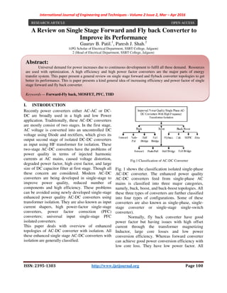
  • 1. International Journal of Engineering and Techniques - Volume 2 Issue 2, Mar – Apr 2016 ISSN: 2395-1303 http://www.ijetjournal.org Page 100 A Review on Single Stage Forward and Fly back Converter to Improve its Performance Gaurav B. Patil.1 , Paresh J. Shah.2 1(PG Scholar of Electrical Department, SSBT College, Jalgaon) 2 (Head of Electrical Department, SSBT College, Jalgaon) I. INTRODUCTION Recently power converters either AC-AC or DC- DC are broadly used in a high and low Power application. Traditionally, these AC-DC converters are mostly consist of two stages. In the first stage, AC voltage is converted into an uncontrolled DC voltage using Diode and rectifiers, which gives its output second stage of isolated DC-DC converters as input using HF transformer for isolation. These two-stage AC-DC converters have the problems of power quality in terms of injected harmonic currents at AC mains, caused voltage distortion, degraded power factor, high crest factor, and large size of DC capacitor filter at first stage. Though all these concern are considered. Modern AC-DC converters are being developed in single-stage to improve power quality, reduced number of components and high efficiency. These problems can be avoided using newly developed single-stage enhanced power quality AC-DC converters using transformer isolation. They are also known as input current shapers, high power-factor single-stage converters, power factor correction (PFC) converters; universal input single-stage PFC isolated converters. This paper deals with overview of enhanced topologies of AC-DC converter with isolation. All these enhanced single stage AC-DC converters with isolation are generally classified. Fig.1 Classification of AC-DC Converter Fig. 1 shows the classification isolated single-phase AC-DC converter. The enhanced power quality AC-DC converters feed from single-phase AC mains is classified into three major categories, namely, buck, boost, and buck-boost topologies. All these three types of converters are further classified into four types of configurations. Some of these converters are also known as single-phase, single- stage converter or single-stage single-switch converter). Normally, fly back converter have good power factor but having issues with high offset current through the transformer magnetizing Inductor, large core losses and low power conversion efficiency. Whereas forward converter can achieve good power conversion efficiency with low core loss. They have low power factor. All RESEARCH ARTICLE OPEN ACCESS Abstract: Universal demand for power increases due to continuous development to fulfil all these demand. Resources are used with optimization. A high efficiency and high power factor converters are the major parts of energy transfer system. This paper present a general review on single stage forward and flyback converter topologies to get better its performance. This is paper presents a kind general idea of increasing efficiency and power factor of single stage forward and fly back converter. Keywords — Forward-Fly back, MOSFET, PFC, THD
  • 2. International Journal of Engineering and Techniques - Volume 2 Issue 2, Mar – Apr 2016 ISSN: 2395-1303 http://www.ijetjournal.org Page 101 these limitations can be achieved by combining both topologies in same package. II. LITRATURE REVIEW In this paper, a high efficiency and high power factor single-stage balanced forward-flyback converter merging a forward and fly back converter topologies is studied. The conventional AC/DC fly back converter can achieve a good power factor but it has a high offset current through the transformer magnetizing inductor, which results in a large core loss and low power conversion efficiency. And, the conventional forward converter can achieve the good power conversion efficiency with the aid of the low core loss but the input current dead zone near zero cross AC input voltage deteriorates the power factor. On the other hand, since the proposed converter can operate as the forward and fly back converters during switch on and off periods, respectively, it cannot only perform the power transfer during an entire switching period but also achieve the high power factor due to the fly back operation. Moreover, since the current balanced capacitor can minimize the offset current through the transformer magnetizing inductor regardless of the AC input voltage, the core loss and volume of the transformer can be minimized. Therefore, the proposed converter features a high efficiency and high power factor. To confirm the validity of the proposed converter, theoretical analysis and experimental results from a prototype of 24W LED driver are presented. [1, 3] Fly-back converters have been widely used because of the irrelative simplicity and their excellent performance for multi output applications. They can save cost and volume compared with the other converters, especially in moderate low power applications. In a fly-back converter, a transformer is adopted to achieve galvanic isolation and energy storage. [2] Global energy consumption tends to grow continuously. To satisfy the demand for electric power against a background of the depletion of conventional, fossil resources the renewable energy sources are becoming more popular. According to the researches despite its fluctuating nature and weather dependency the capacity of renewable resources can satisfy overall universal demand for power. High gain DC/DC converters are the key part of renewable energy systems .The designing of high gain DC/DC converters is compulsory by severe demands. The power conditioning systems for the photovoltaic power sources needs high step- up voltage gain due to the low output of the generating sources. A high step-up topology employing a Series-connected Forward-Fly Back converter, which has a series-connected output for high boost voltage-transfer gain. Series-connected Forward-Fly Back converter is a hybrid type of forward and fly back converter. By stacking the outputs of them extremely high voltage gain can be obtained with small volume and high efficiency with a galvanic isolation. The separated secondary windings reduce the voltage stress of the secondary rectifiers and results in high efficiency.[4] In order to reduce output voltage ripple, it is a common practice to place a large electrolytic capacitor at the output of the conventional, single phase capacitive rectifier. This results in power converter with poor power factor and high total harmonic distortion (THD). In recent years, many high frequency power factor correction (PFC) circuits and current shaping control techniques were developed to meet certain standards. [5] The Fly back converter can both step up and step-down the input voltage, while maintaining the same polarity and the same ground reference for the input and output. MOSFETs are used as a switching device in low power and high frequency switching applications. It may be noted that, as the turn-on and turn-off time of MOSFETs are lower as compared to other switching devices, which reduces the switching losses. High frequency operation of MOSFET reduced size of filters components. These converters are now being used for various applications, such as Switched Mode Power Supply (SMPS) etc. Due to designing and tuning of Fly back converters it can be used to designing of an optimized controller for isolated DC-DC Fly back converter for constant voltage applications. [6] The Zero Voltage Switching (ZVS) technique is used to achieve soft switching. A bidirectional boost converter is connected with an output module as a Parallel Input Serial Output configuration. The flyback converter with Voltage Doubler Rectifier (VDR) acts as an output module.
  • 3. International Journal of Engineering and Techniques - Volume 2 Issue 2, Mar – Apr 2016 ISSN: 2395-1303 http://www.ijetjournal.org Page 102 This connection makes a bidirectional boost converter an active clamp circuit which is connected to the output side in order to extend the step up ratio. A converter with active clamp technique is used to recycle the leakage energy, to eliminate voltage spike due to coupled inductors and also to provide a mechanism to achieve ZVS. To overcome the efficiency degradation during light load due to load dependent soft switching of the ZVS, a control method using Pulse Width Modulation (PWM) proportional to the load current is used.[7] A zero-voltage switching (ZVS) forward- flyback DC-DC converter, which is able to process and deliver power efficiently over a wide input voltage variation. The converter operates at boundary mode between current continuous and discontinuous mode to achieve ZVS. Variable frequency with fixed off time is used for reducing core losses of the transformer, achieving high efficiency.[10] A new bridgeless buck PFC rectifier that substantially improves efficiency at low line of the universal line range is introduced. By eliminating input bridge diodes, the proposed rectifier’s efficiency is further improved. Moreover, the rectifier doubles its output voltage, which extends useable energy of the bulk capacitor after a drop- out of the line voltage.[9] III. CONCEPT OF FLY BACK CONVERTER Fly-back converter is the most commonly used SMPS circuit for low output power applications where the output voltage needs to be isolated from the input main supply. The output power of fly- back type SMPS circuits may vary from few watts to less than 100 watts. The overall circuit topology of this converter is considerably simpler than other SMPS circuits. Input to the circuit is generally unregulated dc voltage obtained by rectifying the utility ac voltage followed by a simple capacitor filter. The circuit can offer single or multiple isolated output voltages and can operate over wide range of input voltage variation. In respect of energy-efficiency, fly-back power supplies are inferior to many other SMPS circuits but its simple topology and low cost makes it popular in low output power range. The commonly used fly-back converter requires a single controllable switch like, MOSFET and the usual switching frequency is in the range of 100 kHz. A two-switch topology exists that offers better energy efficiency and less voltage stress across the switches but costs more and the circuit complexity also increases slightly. The present lesson is limited to the study of fly-back circuit of single switch topology. Fig.2 shows the basic topology of a fly-back circuit. Input to the circuit may be unregulated dc voltage derived from the utility ac supply after rectification and some filtering. The ripple in dc voltage waveform is generally of low frequency and the overall ripple voltage waveform repeats at twice the ac mains frequency. Fig.2. Basic Topology of Fly-Back Converter. Since the SMPS circuit is operated at much higher frequency (in the range of 100 kHz) the input voltage, in spite of being unregulated, may be considered to have a constant magnitude during any high frequency cycle. A fast switching device („S‟), like a MOSFET, is used with fast dynamic control over switch duty ratio (ratio of ON time to switching time-period) to maintain the desired output voltage. The transformer, in Fig.2, is used for voltage isolation as well as for better matching between input and output voltage and current requirements. IV. CONCEPT OF FORWARD CONVERTER Forward converter is another popular switched mode power supply (SMPS) circuit that is used for producing isolated and controlled dc voltage from the unregulated dc input supply. The forward converter, when compared with the fly-back circuit,
  • 4. International Journal of Engineering and Techniques - Volume 2 Issue 2, Mar – Apr 2016 ISSN: 2395-1303 http://www.ijetjournal.org Page 103 is generally more energy efficient and is used for applications requiring little higher power output (in the range of 100 watts to 200 watts). However the circuit topology, especially the output filtering circuit is not as simple as in the fly-back converter Fig.3 shows the basic topology of the forward converter. It consists of a fast switching device ‘S’ along with its control circuitry, a transformer with its primary winding connected in series with switch ‘S’ to the input supply and a rectification and filtering circuit for the transformer secondary winding. The load is connected across the rectified output of the transformer-secondary. Fig.3. Basic forward converter topology The transformer used in the forward converter is to be an ideal transformer with no leakage fluxes, zero magnetizing current and no losses. The basic operation of the circuit is explained with different mode operation here assuming ideal circuit elements. In fact, due to the presence of finite magnetizing current in a practical transformer, tertiary winding needs to be introduced in the transformer and the circuit topology changes slightly. V. SINGLE SWITCH CONVERTER PFC circuit can be available in two forms, i.e. single stage and two –stage scheme in two stage schemes. In two stage scheme, AC-DC converter is connected to the line to provide good input power factor and generate regulated dc voltage. Generally this voltage cannot directly supply the load since it contains intolerable second harmonic content. Therefore a ac/dc converter is cascade to tightly regulate the output voltage. These two power stages are controlled separately. And thus it makes optimization of both converters possible. The main drawbacks of this scheme are its higher cost and larger size resulting from its increased component number and complicated control circuits. The one – stage PFC scheme combines the PFC circuit and the voltage regulation circuit in one stage. Due to the simplified power stage and control circuit of the single stage scheme, it is attractive to many applications with cost size. Fig. 4. InputV-I characteristics of basic flyback converter operating in DCM. (a) Flyback converter in PFC application. (b) Input current. (c) Input V-I characteristics. Fig.5. Basic circuit schematic of proposed converter. The isolated flyback converter circuit and its input current waveform are shown in Fig. 4. (a) and (b), respectively.[5] Since switching frequency, it is reasonable to assume that the line voltage is constant in a switching cycle. The basic circuit schematic of proposed new single stage single switch isolated converter is shown in Fig.5.[5] The input circuit employs a Flyback topology and the output circuit is a forward converter. The power switch and storage capacitor
  • 5. International Journal of Engineering and Techniques ISSN: 2395-1303 are placed between the two circuits with diode D1 and D2 coordinating their two separate operations. Table 1. Time intervals and staus of devices in mode operation Mode Time interval Conducting device S D 1 D 2 D 3 M1 to<t<t1 × × M2 t1≤t≤t’2 × × t'2≤t≤t2 × M3 t2≤t≤to +Ts It can be shown that in steady state the converter operates in three operation modes du switching cycle. Table1. Shows three modes of operations. According to corresponding times and the status of the switching devices. Fig.6. Theoretical key waveforms of proposed converter. Typical steady state operation waveforms are shown in fig. 6. Which consist of three modes can be deeply studied with table1 having output filter maintains the output voltage until next switching cycle begins. Considering all design parameters i.e. maximum duty ratio, magnetizing inductance, transform ratio, selection of capacitor, filter inductance, power switch and diodes. The waveforms of filtered line current, switch voltage and current through diodes D1 were recorded at International Journal of Engineering and Techniques - Volume 2 Issue 2, Mar – http://www.ijetjournal.org laced between the two circuits with diode D1 and D2 coordinating their two separate operations. Table 1. Time intervals and staus of devices in Conducting device D 4 D 5 × × × × It can be shown that in steady state the converter operates in three operation modes during one three modes of corresponding times and . Theoretical key waveforms of proposed on waveforms are . Which consist of three modes can be deeply studied with table1 having output filter til next switching cycle begins. Considering all design parameters i.e. maximum duty ratio, magnetizing inductance, transform ratio, selection of capacitor, filter inductance, power switch and diodes. The waveforms of filtered line current, switch voltage and current through diodes D1 were recorded at peak line voltage. It is found that simulated and experimental waveforms are in a good agreement. The line current waveforms are and in phase with the line voltage, proving that good power factor was achieved by this converter topology. Fig.7. represents measu and efficiency under different load condition. (a) Input power factor (b)Efficiency Fig.7. Experimental efficiency and input power factor. VI. Conventional single stage PFC converter Recently, conventional single- factor correction) LED drivers which are well known as most cost solutions. Fig.9. shows their transformer magnetizing inductor currents. As shown in this figure, the magnetizing inductor offset current of fly back converter is larger than that of forward – Apr 2016 Page 104 peak line voltage. It is found that simulated and experimental waveforms are in a good agreement. waveforms are almost sinusoidal and in phase with the line voltage, proving that ctor was achieved by this converter asured power factor and efficiency under different load condition. (a) Input power factor efficiency and input power factor. Conventional single stage PFC converter -stage PFC (power factor correction) LED drivers shown in fig. 8, which are well known as most cost effective shows their transformer magnetizing inductor currents. As shown in this figure, the magnetizing inductor offset current of fly back converter is larger than that of forward
  • 6. International Journal of Engineering and Techniques - Volume 2 Issue 2, Mar – Apr 2016 ISSN: 2395-1303 http://www.ijetjournal.org Page 105 converter. The magnetizing inductor offset current of fly back and forward converter is < , >= ˳ ( ) (1) < , >= 1 + ! "# $%& '^2*+ (2) (a) Single-stage flyback converter (a) Single stage forward converter Fig 8 Conventional single stage PFC converter circuits Moreover, from equations (1) and (2), while the magnetizing inductor offset current of flyback converter is dependent on the load current Io, that of forward converter is not. Therefore, as the load current is more increased, the offset current of flyback converter becomes larger, which might result in the larger core loss and volume of transformer. For these reasons, the forward converter is superior to the flyback converter in terms of the transformer size and energy conversion efficiency. Fig.9. Transformer magnetizing inductor currents of conventional flyback and forward converters Fig 10.PFC performance of forward and flyback In the meanwhile, as shown in Fig. 10, while the flyback converter can transfer the input energy to the output side over an entire range of input voltage, the forward converter cannot at the lower input voltage than the reflected output voltage nVo to the transformer primary side. This is because the forward converter is originated from the step-down buck topology. Therefore, the input current dead zone near zero cross AC input voltage is always observed and deteriorates the power factor in the forward converter. Therefore, the flyback converter is superior to the forward converter in terms of the PFC performance.
  • 7. International Journal of Engineering and Techniques - Volume 2 Issue 2, Mar – Apr 2016 ISSN: 2395-1303 http://www.ijetjournal.org Page 106 VII. Proposed single stage PFC forward flyback converter To solve all these problems, a high efficiency and high power factor single-stage balanced forward- flyback converter is proposed as shown in Fig.11. Since the proposed converter merges the forward and flyback topologies, it can operate as the forward and flyback converters during switch turn- on and off periods, respectively. Therefore, it cannot only perform the power transfer during an entire switching period but also achieve the high power factor. Especially, since the charge balanced capacitor Cb can make the proposed converter perform the forward operation regardless of the input voltage, the magnetizing inductor offset current, core loss and transformer size can be minimized. Fig.11. Proposed single stage PFC forward flyback converter circuit Fig. 11 shows the circuit diagram of the proposed forward flyback converter.[1] As shown in this figure, its primary side is exactly same as that of the conventional flyback converter consisting of one power switch (M1) and one transformer. On the other hand, its secondary side consists of one output inductor (Lo) for forward operation, one DC blocking capacitor (Cb) for balancing operation and three output Diodes (D1, D2, D3). When M1 is conducting, the proposed converter operates as a forward converter. On the other hand, when M1 is blocked, the proposed converter operates as a flyback converter. However, if it is assumed that the proposed converter has no balancing capacitor Cb, abovementioned forward operation is possible only when the reflected primary voltage Vin/n to the transformer secondary side is higher than the output voltage Vo. This is because the forward converter is originated from the buck converter. Therefore, the forward-flyback converter operates only as a flyback converter over the range of Vin/n < Vo. Especially, at the minimum input voltage near Vin=90Vrms, Vin/n is lower than Vo during most of periods and thus, the transformer has a large magnetizing offset current similar to the conventional flyback converter. In this case, the transformer core loss and volume are also as large as those of the conventional flyback converter. On the other hand, if the balancing capacitor Cb is serially inserted with the transformer secondary side, it can make the average current through Cb during forward operation become exactly same as that during flyback operation by the charge balance principle of Cb. In other words, since the voltage across Cb charged by flyback operation is added to the Vsec=Vin/n during forward operation, Vin/n+Vcb becomes higher than Vo and thus, the forward operation is possible even at Vin/n<Vo (a) (b) Fig.12. Primary and magnetizing currents of forward-flyback converter according to the input voltage. (a) Without balancing capacitor (b) with balancing capacitor Therefore, the proposed forward-flyback converter with the balancing capacitor Cb can always operate as both forward and flyback converters regardless of the input voltage. Fig.12. shows the primary and magnetizing current waveforms of the proposed converter operating in the boundary conduction mode (BCM). And, Fig.12 (a) and (b) show current waveforms without and with balancing capacitor Cb according to the input voltage, respectively. As mentioned earlier, the proposed converter with Cb can operate as both forward and flyback converters over an entire range of input voltage with the aid of Vcb. On the other
  • 8. International Journal of Engineering and Techniques - Volume 2 Issue 2, Mar – Apr 2016 ISSN: 2395-1303 http://www.ijetjournal.org Page 107 hand, while the proposed converter without Cb can transfer the input energy to the output side at Vin/n>Vo, it cannot at Vin/n<Vo. As a result, the proposed converter with balancing capacitor Cb features a smaller magnetizing offset current, resultant smaller core loss and more reduced transformer volume. Fig.13. Key waveforms of the proposed forward – flyback converter The circuit operation of the proposed converter is basically divided into two modes according to the conduction state of each switch as shown in fig.13. first mode operation from time interval t0-t1 and second from t1-t2. By considering all design parameters regarding proposed converter its performance is observed. Which also compared with conventional proposed individual converters and analysis conclude that it is suitable for low power application. For experimental performance of converter it’s operated with different root mean square values of voltage and efficiency and power factor is observed. Fig.14. Comparisons of efficiency and power factor between flyback and proposed forward-flyback converter Fig. 14 shows the measured efficiency and power factor of the proposed forward-flyback and conventional flyback converters. As shown in this figure, the proposed converter has the high power factor above 95% over a wide range of input voltage. Especially, its efficiency along wide input voltage range is above 88.71% and higher than the conventional converter by maximum 8.07% at 264Vrms. This high efficiency is due primarily to the small transformer offset current and resultant reduced core loss. VIII. CONCLUSION This paper discusses various topologies employed for improvement of performance AC-DC converter. Initially conventional forward flyback converter uses two Transformers. This is having problems regarding size and cost due to large number circuit component. In order to overcome these drawbacks of two stage scheme. One stage PFC scheme adopted which combines fly back and forward circuit in single stage it makes optimization of converter in single package. Another issues of magnetizing offset current , core loss are overcome with single stage balanced forward –flyback type proposed converter .which have current balanced capacitor can minimize the offset current all the way through the transformer magnetizing inductor apart from input AC voltage and reduce core loss. After this review we realized that single stage
  • 9. International Journal of Engineering and Techniques - Volume 2 Issue 2, Mar – Apr 2016 ISSN: 2395-1303 http://www.ijetjournal.org Page 108 scheme is outstanding solution for low power application. It also provides good power factor and efficiency. REFERENCES [1] Yoon choi, Moon- Keum and Sang Kyoohan ,jeong-ilkang, “ High efficiency and High Power Factor Single Stage Balanced Forward – Fly back Converter”, Proceeding of the IEEE, pp. 822-827, 2013. [2] Subhrajyoti Modak , Goutam Kumar Panda, Pradip Kumar Saha and Sanskar Das , “Design of Novel fly-back converter using PID controller” Proceeding of IJAREEIE, Vol.4, pp. 289-297,Jan 2015. [3] M. Venkatesh Kumar and K. Chandra, “Power Factor Improvement using Single Stage Balanced Forward Flyback Converter” Proceeding of IJIT, Vol.3, No.4, pp. 640-645, July 2015. [4] J. Lee, J. Park, H. Jeon, “Series-Connected Forward–Flyback Converter for High Step-Up Power Conversion,” IEEE Trans. Power Electronics, Vol.26, No.12, pp.3629-3641, Dec. 2011. [5] Hua-Min Xu, Xin-Bo Ruan, Yang-Guang Yan “ A Novel Forward Single-Stage Single-Switch Power Factor Correction AC/DC converter”, Proceeding of PESC, Vol.2, pp. 754-759, 2001. [6] Abhinav Dogra, Kanchan pal, “Designing and Tuning of PI Controller for Flyback Converter”, Proceeding of IJETT, Vol. 13 No.3, Jul 2014. [7] R. Sudha and P.M. Dhanasekaran, “DC—DC Converter Using PID Controller and Pulse Width Modulation Technique”, Proceeding of IJETT, Vol.7, No.4, pp165-168, Jan 2014. [8] Yonghan Kang, Byungcho Choi and Wonseok Lim, "Analysis and Design of a Forward-Flyback Converter Employing Two Transformers", Proceeding of the IEEE, Vol. 1, pp. 357-362, June. 2001. [9] Yungtaek Jang and Milan M. Jovanovic, "Bridgeless Buck PFC Rectifier", Proceeding of the APEC2010, pp. 23-29, Feb. 2010. [10] F. Chen, E. Auadisian, J. Shen and I. Batarseh, "Soft switching Forward-Flyback DC-DC Converter", Proceeding of JECE, Vol.3, No.5, pp. 26-35, 2013. [11] Sanjeevsingh and Bhimsingh,“ Comprehensive study of single phase AC-DC power corrected converter with High frequency isolation” ,IEEE trans. On Industrial Informatics, Vol. 7, No. 4, pp. 540-556, Nov 2011.