SlideShare a Scribd company logo
1 of 14
Download to read offline
International Journal of Power Electronics and Drive Systems (IJPEDS)
Vol. 9, No. 1, March 2018, pp. 443 – 456
ISSN: 2088-8694 443
Institute of Advanced Engineering and Science
Side Effects of Damping Element Insertion in LCL Filter
for DC/AC Inverter
Faizal Arya Samman, Ma’arif Hasan, Tirza Damayanti
Department of Electrical Engineering, Faculty of Engineering
Universitas Hasanuddin, Indonesia
Article Info
Article history:
Received Aug. 18, 2017
Revised Dec. 11, 2017
Accepted Dec. 28, 2017
Keyword:
Power Converter
DC/AC Inverter
Passive Filter
Harmonics
Resonance Damping Circuit
ABSTRACT
The negative impacts or side effects of a damper circuit insertion in an LCL passive
filter utilized to filter DC/AC inverters output voltage is presented in this paper. For
comparative study, this paper discusses two damping configurations, namely series
and parallel damping, as well as the LCL filter without damping element. Four cri-
teria are used to explore the impacts of the damper circuits, i.e. their total harmonic
distortions (THDs), the output voltage amplitude, the output power and the power effi-
ciency. Theoretically and empirically shown by previous studies, the damper element
insertion in the filter circuit can indeed reduce the peak resonance frequency of the fil-
ter in its frequency response curve. Nevertheless, the damper insertion can potentially
decrease the inverters power output and power efficiency, voltage output amplitude,
and in circumstances cannot improve its THD reduction. The analysis results have
shown that the side effects depends also on the load conditions, which are different for
each damping circuit configuration.
Copyright c

 2018 Institute of Advanced Engineering and Science.
All rights reserved.
Corresponding Author:
Faizal Arya Samman
Universitas Hasanuddin, Faculty of Engineering, Dept. of Electrical Engineering
Kampus Gowa, Jl. Poros Malino Km. 6, Bontomarannu 92171, Sulawesi Selatan, Indonesia
Email: faizalas@unhas.ac.id
1. INTRODUCTION
Nowadays, the increase of electricity demands, the decrease of the fossil fuels supply and the need for
cleaner environments have catalyzed the urgent need for renewable energy sources. Renewable energy sources
such as solar or sunlight are strategically advantageous for countries having sunny atmospheric conditions,
i.e. the countries lies around the earth equatorial area. Meanwhile, researches in the area of solar-cells or
photovoltaic (PV) systems have been intensively made with special intention on the improvement of their
energy efficiency. In the future, the higher solar efficiency improvement will boost the rapid use the solar cell
not only for industries but specially for home scale utilization. The fabrication cost of solar cells should also
be decreased to reduce their cost in markets.
Solar-based power plants have been established in many areas and countries. There are some important
components of a solar-based power plant. One of them is inverter, beside a charge controller and an energy
storage unit such as rechargeable battery. Figure 1a presents a photovoltaic (PV) system with alternating current
(AC) load. The charge controller consists of a Maximum Power Point Tracer (MPPT) module and a battery
charger circuit. The MPPT module is used to maximize electric energy or power transfer from PV panel to the
battery unit. Because most of renewable energies have direct current (DC) power outputs, inverters becomes
an important component in a renewable-energy-based power plant. Inverter is an electric device that works to
change or convert DC to AC voltages. There are some techniques to design an inverter. One of them is by
using a full-bridge circuit incorporating four power electronic switch devices, where four gate terminals of the
switching devices are controlled by an electronic control unit.
Journal Homepage: http://iaescore.com/journals/index.php/IJPEDS
Institute of Advanced Engineering and Science
w w w . i a e s j o u r n a l . c o m
, DOI: 10.11591/ijpeds.v9.i1.pp443-456
444 ISSN: 2088-8694
MPPT
Module
Battery
Charger
Battery
Unit
DC/AC
Inverter
+ Filter
Load 220V/
50Hz/60Hz
Solar Array
VDC2
VDC3
VDC1
VAC
VDC0
Charge Controller Unit
Discussion
Domain
(a) Photovoltaic system
Filter
9
10
17
7
1
2
4
V
BATTERY
M1
M2
M3
M4
5
3
7
8
6
0
NMOS
Driver
NMOS
Driver
NMOS
Driver
NMOS
Driver
Load
Electronic Control Unit (ECU)
D1
D2 D4
D3
C
A A
(b) inverter circuit topology
Figure 1. The photovoltaic system and the DC/AC inverter and filter topology.
There many challenging problems in designing an inverter. Some of them are summarized in the
following items.
• Power efficiency and switching loss due existing switching mechanism
• Unbalance voltage due to unbalance loads in 3-phase inverter applications
• Voltage amplitude and power factor shifting due to loading conditions
• Grid synchronizations with an existing grid for hybrid power generation
• Total harmonic distortion (THD) due to the used PWM-based switching mechanism to control the in-
verter output
Most of power losses in switched-mode inverter circuits are due to the existing switching mechanism.
Switching pulses applied to the gate terminal of power switching devices will partially convert electrical energy
to be thermal energy. Nowadays, new silicon technologies, such as Power MOSFET based on Silicon Carbide
(SiC) technology can reduce power losses and have longer operating lifetime [1], [2]. Beside Power MOSFET,
another switching device that can be used is Insulated Gate Bipolar Transistor or IGBT. Like power MOSFET,
IJPEDS Vol. 9, No. 1, March 2018: 443 – 456
IJPEDS ISSN: 2088-8694 445
the IGBT operations can also induce higher conductance losses and lower switching performance compared to
SiC-based MOSFET [3]. The switching losses as well as electromagnetic interference can be avoid by a new
concept i.e. by controlling the current and voltage slopes individually for all operating conditions of the IGBTs
[4].
Voltage balancing is also a problem in inverter design especially in grid-connected applications. Stand-
alone Micro Grid (MG) tends to have unbalancing voltage affected by the unbalanced load in single phase. To
achieve the balancing of phase voltage, each single phase inverter can be controlled independently [5]. Other
important aspects in inverter design are the output voltage amplitude, power efficiency and grid synchroniza-
tion. Grid synchronization is especially very important in 3-phase grid-connected inverter applications [6].
The use of pulse width modulation (PWM) control systems, for instance in AC motor control appli-
cations, causes the appearance of common mode voltage (CMV) at the neutral point. CMV suppression and
elimination without influencing the inverter’s output voltage and better THD can be reached by using a special
technique namely Partial elimination SVPWM (PE-SVPWM) and full elimination SVPWM (FE-SVPWM).[7].
The used of a coupled inductor multiplier can also reduce the conduction losses, due to the CMV at neutral
point, and raise the efficiency [8]. Z-source T-type inverter is an example way to raise the efficiency system and
to boost voltage level without any additional DC-DC converter or transformer. The method makes the output
current of inverter are sinusoidal and synchronous with the grid frequency and its phase [9].
Leakage current is the drawbacks of grid-tied transformerless inverter systems. It produces system
losses and inject harmonics into the grid [10], [11]. Therefore, the use of passive filter is important to imple-
ment. The THD existence causes the inverter output voltage not be able to become pure sine wave as expected.
To suppress the harmonic distortion, a passive filter is coupled to the output terminal of the inverter. According
to the IEEE Standard, the acceptable THD of the inverter output voltage should be below 5% [12].
There are many filters that can be used to suppressed the THD, such as L, LC, LCL, LLCL, etc
[13], [14], [15]. Among the aforementioned filters, the LCL filter has better capability to suppress harmonic
distortion [16], [15]. Adding an LCL passive filter to the output terminal of an inverter can cause an appearance
of peak resonance frequency. This phenomena can make the inverter system unstable and its performance
becomes weak. Therefore, to suppress the resonance effect of the LCL passive filter, a resistance component as
damper is inserted into the filter circuit. The resistance component inserted to the LCL passive filter is called
as a resistance damping [17].
Multi-level inverters are also another type of inverter, which is proposed to reduce harmonics [18],
[19] [20]. Multi-level inverter has multiple output voltage levels, which is enabled by the use of multiple DC
source. In renewable energy applications, the design cost of a multi-level inverter is higher compared to a
single-level inverter, due to the need for more DC/DC converters to maintain the voltage levels of the multiple
DC sources. Single-level inverters are still favorable, since they are more simple with lower design cost.
2. RELATED WORKS AND CONTRIBUTION
This paper will particularly discuss an LCL filter analysis. Since the use of LCL passive filter causes
the appearance of resonant effect, a damping element is used. By using the damping element, the effect of
resonant can be suppressed [17], [21]. However, the resonance damping resistor will raise an extra power loss,
reduce maximum voltage amplitude and weaken the high-frequency harmonic reduction capability. This paper
will show a comparative study on a few filter circuit with and without damping element. The LCL passive
filter with and without the resistance damping tested with resistance loads. The criteria used in this study are
the capability of LCL passive filter with and without resistance damping in reducing the harmonic distortion,
maintaining the maximum output voltage amplitude and average output power as well as the power efficiency
of inverters and filters.
To the best of the author’s knowledge, the study of this paper, which is based on concurrent analysis
of those four criteria with variable (resistance) loads, has not been explored by the previous works. The work
in [17], for example, investigates many filters with active and passive damping methods. The work in [22]
proposes different passive damping tuning methods and its analytical damping losses estimation. Nevertheless,
both do not expose the impact of the resonance damping element insertion for different load conditions with
extra side effects analysis on the THD, power output, power efficiency and the output voltage amplitudes.
Variable loading conditions should be taken into account, since in practical conditions, the load is unknown
and can potentially affect the load voltage and load current variables. Moreover, the load can be topologically
Side Effects of Damping Element Insertion in LCL ... (Faizal Arya Samman)
446 ISSN: 2088-8694
involved as the part of the filter.
3. RESEARCH METHOD
To achieve the research objective, systematical steps are used to explore the filter and inverter circuit
characteristics. The filter and inverter are modeled in (Simulation Program with Integrated Circuit Emphasis).
The transfer function of the filter is also mathematically modeled and then numerically modeled to obtain the
frequency response curves. By using a SPICE simulator, the inverter+filter circuits are simulated for different
load impedance values to measure some parameters and variables, i.e.
1. The THD or total harmonic distortion of the filter output voltages. The analysis is made for 100 harmonic
frequency values, where 50 Hz is set as the base frequency.
2. The voltage amplitude values at the inverter’s input and output terminals, as well as at the filter output
terminal.
3. The average output powers at the inverter’s input and output terminals, as well as at the filter output
terminal.
4. The power efficiency of the inverter output power over the inverter input power, the filter output power
over the inverter output power, and the efficiency of the filter output power over the inverter input power.
After collecting the simulation data, the characteristic curves of all four aforementioned simulation
parameters relative to the changes of load impedance values are plotted, and then some concluding remarks are
given.
4. FILTER MODELING AND ANALYSIS
The simulated inverter and filter circuit is presentedg in Figure 1b. The inverter as well as the filter
circuit is modelled in SPICE. The electronic control unit (ECU) as shown in the figure generates four sinusoidal
pulse width modulation (SPWM) signals. The voltage level of the SPWM signals is amplified using NMOS
gate driver such that it can drive the n-channel power MOSFET at the points 3, 5 , 6 and 8, respectively as
shown in Figure 1b.
Each two of the SPWM signals has similar phase and waveform. The waveform of SPWM signals at
the points 3 and 8 is similar, while the other one at the points 5 and 6 is also similar. The NMOS driver increases
the voltage level to effectively drive the NMOS gate terminal. In general this driver separates optically the
power converter circuit (having higher power) with the electronic control unit (having lower power), or is used
to protect the ECU from the higher power circuit.
In order to generate a sine waveform from the output terminal of the inverter, we need to generate
some signals to control the process. Normally, this process is made under control of the ECU. The ECU should
be programmed to generate two sine-based pulse width modulation (SPWM) as presented by the curves at the
second and third line plots in Figure 2. In order to generate the SPWM signals, there are some techniques
that can be used. One of them is illustrated from the curves at the first line plot in the Figure 2. An absolute
sine wave, called as modulating signal (Vmod), is generated having 50 Hz frequency, as well as a carrier signal
(Vcarr) in sawtooth waveform. The figure presents the carrier signal with 20 sawteeth in every half period of
the sine wave signal. Both signal are compared each other to generate the SPWM using the following rule.
When Vcarr > Vmod then Vgate = 0, else Vgate = 5 V . We assume that the logic ’1’, generated by the ECU,
is related to 5 V. During the first half period of the sine wave signal, the SPWM signal is applied to the gates
of MOSFET M1 and M4. Then, during the next second half period, the SPWM signal is applied to the gates
of MOSFET M2 and M3. Consecutively applying this periodic waveform to the MOSFET gate terminals, then
we will have the inverter’s output voltage as shown in the fourth line plot in the Figure 2. It seems that the
inverter generates AC signal but with large total harmonic distortion (THD).
Because, the output voltage of the inverter contains the THD value larger than 5%, then a filter circuit
is required to decrease the THD below 5%. There many types of filters that can be used to suppress the THD. In
general, the filter can classified as active and passive filters. Active filters are rarely used due to the complexity
of circuit, especially for high power applications. Passive filters are mostly used in industries because of their
IJPEDS Vol. 9, No. 1, March 2018: 443 – 456
IJPEDS ISSN: 2088-8694 447
0 0.005 0.01 0.015 0.02 0.025
0
0.5
1
Inverter Output without Filter (20 sawteeth per half period)
Vcarr
Vmod
(V)
Carrier Voltage
Modulator Voltage
0 0.005 0.01 0.015 0.02 0.025
0
2
4
6
Vgate1,4
(V)
0 0.005 0.01 0.015 0.02 0.025
0
2
4
6
Vgate2,3
(V)
0 0.005 0.01 0.015 0.02 0.025
−20
0
20
Inv.
Vout
(V)
Time (second)
Figure 2. The inverter output signal generation without filter by using 20 sawteeth per half period (The THD
of the inverter’s output voltage is 47.829%).
simple use and low cost utilization. the discussion about the used filters to suppress the THD is presented in
the following sub section.
Rds
L1
C
L2
ZL
Filter + series damper Load
Vin
Vout
(b)
L1
C
L2
ZL
Filter without damper Load
Vin
Vout
(a)
Rdp
L1
C
L2
ZL
Filter + par. damper Load
Vin
Vout
(c)
Vd Vd Vd
Figure 3. The circuit configuration of the filters under evaluation: (a) filter without damping, (b)(c) filters with
passive series and parallel damping methods [17].
4.1. Filter Model without Damper
The filter model without a damper element is presented in Figure 3(a). The transfer function of the
Vout(s)
Vd(s) is as follows.
Side Effects of Damping Element Insertion in LCL ... (Faizal Arya Samman)
448 ISSN: 2088-8694
Vout(s)
Vd(s)
=
ZL
sL2 + ZL
(1)
The transfer function of the Vd(s)
Vin(s) is as follows.
Vd(s)
Vin(s)
=
1
s2L1C + 1
(2)
By using the Laplace Transform Characteristic, the transfer function of Vout(s)
Vin(s) can be obtained by multiplying
Eq. (1) and Eq. (2), which results in the following equation.
Vout(s)
Vin(s)
=

ZL
sL2 + ZL
 
1
s2L1C + 1

(3)
Simplifying Eq. (3), we will have the final transfer function form, i.e.
Vout(s)
Vin(s)
=
ZL
s3L1L2C + s2ZLL1C + sL2 + ZL
(4)
4.2. Filter Model with Series Damper
The filter model with a damper element inserted in series with the C-element of the filter is presented
in Figure 3(b). Zds is obtained by deriving the equivalent impedance between the C-element and the series
resistant damper Rds, i.e.
Zds = Rds +
1
sC
=
sRdsC + 1
sC
(5)
The transfer function of the Vout(s)
Vd(s) is the same result presented in Eq. (1). The transfer function of
the Vd(s)
Vin(s) is as follows.
Vd(s)
Vin(s)
=
Zds
sL1 + Zds
=
sRdsC + 1
s2L1C + sRdsC + 1
(6)
By using the Laplace Transform Characteristic, the transfer function of Vout(s)
Vin(s) can be obtained by multiplying
Eq. (1) and Eq. (6), which results in the following equation.
Vout(s)
Vin(s)
=

ZL
sL2 + ZL
 
sRdsC + 1
s2L1C + sRdsC + 1

(7)
Simplifying Eq. (7), we will have the final transfer function form, i.e.
Vout(s)
Vin(s)
=
sZLRdsC + ZL
s3L1L2C + s2(ZLL1C + RdsL2C) + s(L2 + ZLRdsC) + ZL
(8)
4.3. Filter Model with Parallel Damper
The filter model with a damper element inserted in parallel with the C-element of the filter is presented
in Figure 3(c). Zdp is obtained by deriving the equivalent impedance between the C-element and the series
resistant damper Rdp, i.e.
Zds =
Rdp
1
sC
Rdp + 1
sC
=
Rdp
sRdpC + 1
(9)
The transfer function of the Vout(s)
Vd(s) is the same result presented in Eq. (1). The transfer function of
the Vd(s)
Vin(s) is as follows.
IJPEDS Vol. 9, No. 1, March 2018: 443 – 456
IJPEDS ISSN: 2088-8694 449
Vd(s)
Vin(s)
=
Zdp
sL1 + Zdp
=
Rdp
s2RdpL1C + sL1 + Rdp
(10)
By using the Laplace Transform Characteristic, the transfer function of Vout(s)
Vin(s) can be obtained by multiplying
Eq. (1) and Eq. (10), which results in the following equation.
Vout(s)
Vin(s)
=

ZL
sL2 + ZL
 
Rdp
s2RdpL1C + sL1 + Rdp

(11)
Simplifying Eq. (11), we will have the final transfer function form, i.e.
Vout(s)
Vin(s)
=
ZLRdp
s3RdpL1L2C + s2(L1L2 + ZLRdpL1C) + s(ZLL1 + RdpL2) + ZLRdp
(12)
4.4. Frequency Response Characteristic
After obtaining the transfer function of the filter circuits with three different damping element con-
figuration, including the one without damping element, then this subsection presents the frequency response
characteristic of the filters. Figure 4 presents the bode plot comparison of the filter circuits.
10
2
10
3
−20
0
20
40
60
Freq. Response of the Filters (Rds=3 Ohm, Rdp=300 Ohm)
Frequency (rad/s)
Magnitude
10
2
10
3
−200
−100
0
100
200
Frequency (rad/s)
Phase
(deg.)
no damp.
series damp.
parallel damp.
Figure 4. The transfer function of the filter with and without damping.
5. SIMULATION RESULTS AND ANALYSIS
The steady-state and transient analysis or simulation results of some important measured variables
in the inverter plus filter configurations are presented in this section. the simulations are made using SPICE
Side Effects of Damping Element Insertion in LCL ... (Faizal Arya Samman)
450 ISSN: 2088-8694
(Simulation Program with Integrated Circuit Emphasis), which is an industry standard circuit simulator. The
measured parameters are inverter’s and filter’s output voltages, output currents, output powers including the
average output powers. The THD and power efficiency measurements of the inverter and filter circuit are also
made in the analysis.
5.1. Steady-State Point Analysis
In this steady state point analysis or simulation, the measured parameters are THD, voltage and current
amplitudes, output power and power efficiencies. In every simulation run, the circuit is simulated until the
steady-state condition is attained, and then, the parameters are observed from the SPICE output probe windows.
The simulation results are shown in the following sub sections.
5.1.1. THD and Voltage Amplitude Measurements
The upper section of Figure 5 shows the THD measurements at the filter’s output points. Each fig-
ure presents three THD curves comparisons between the inverter+filter circuits without damping, with series
damping and with parallel damping for different resistance loads, i.e. from 100
Ω until 105
Ω. As shown in the
figure, the filter without damping element presents the best THD values, when the load impedance is above
20 Ω. Below that impedance value, the filters with damping elements have better THD values, but all of them
have THD above 5%, the standardized THD limit.
10
0
10
1
10
2
10
3
10
4
10
5
0
5
10
15
20
Resistive Load (Ohm)
THD
(%)
THD Curves, Inverter and Filter Output Voltages
10
0
10
1
10
2
10
3
10
4
10
5
26
Inverter
Vout
(V)
10
0
10
1
10
2
10
3
10
4
10
5
0
100
200
300
Resistive Load (Ohm)
Filter
Vout
(V)
LCL without Damping
LCL with Series Damping
LCL with Parallel Damping
Figure 5. The THD measurements.
The middle and lower sections of Figure 5 shows the voltage amplitude measurements at the inverter’s
and filter’s output points. Each figure presents the curves comparisons between the inverter+filter circuits
without damping, with series damping and with parallel damping for different resistance loads, i.e. from 100
Ω
until 105
Ω. The voltage measurements at the inverter’s input terminal are not presented, since they present
equal value, i.e. 24 V for each aforementioned resistance load value.
IJPEDS Vol. 9, No. 1, March 2018: 443 – 456
IJPEDS ISSN: 2088-8694 451
The filter output voltage amplitudes of the circuit without damping element presents higher values
compared to the filters with series and parallel damping element, especially for the load impedance above
10 Ω. For the load impedance below 10 Ω, all filter circuit presents almost the same results.
5.1.2. Current Measurements
Figure 6 shows the current measurements at the inverter’s and filter’s input-output points. Each figure
presents three current curves comparisons between the inverter+filter circuits without damping, with series
damping and with parallel damping for different resistance loads, i.e. from 100
Ω until 105
Ω. At the upper part
of the figure, the current measurements at the inverter’s input terminal are presented. At the middle part of
the figure, the current measurements at the inverter’s output terminal are presented. At the bottom part of the
figure, the current measurements at the filter’s output terminal are presented.
10
0
10
1
10
2
10
3
10
4
10
5
0
10
20
30
40
Inverter
Iin
(A)
LCL without Damping
LCL with Series Damping
LCL with Parallel Damping
10
0
10
1
10
2
10
3
10
4
10
5
0
5
10
Inverter
Iout
(A)
LCL without Damping
LCL with Series Damping
LCL with Parallel Damping
10
0
10
1
10
2
10
3
10
4
10
5
0
0.5
1
1.5
Resistive Load (Ohm)
Filter
Iout
(A)
LCL without Damping
LCL with Series Damping
LCL with Parallel Damping
Figure 6. The current measurements.
As shown in Figure 6, the circuit with series damping element has better inverter input currents com-
pared to the circuit without damping element and the circuit with parallel damping element. For the load
impedance above 50 Ω, the circuit without damping element has the best inverter output currents. The almost
similar values are presented for the load impedance below 50 Ω. For the load impedance below 5kΩ, the output
current of the filter without damping element has the highest current values. The almost similar filter output
current are presented for the load impedance above 5kΩ.
5.1.3. Power Measurements
Figure 7a shows the power measurements at the inverter’s and filter’s input-output points. Each figure
presents three power curves comparisons between the inverter+filter circuits without damping, with series
damping and with parallel damping for different resistance loads, i.e. from 100
Ω until 105
Ω. At the upper part
of the figure, the power measurements at the inverter’s input terminal are presented. At the middle part of the
figure, the curves present the power measurements at the inverter’s output terminal. At the bottom part of the
figure, the power measurements at the filter’s output terminal are presented.
Side Effects of Damping Element Insertion in LCL ... (Faizal Arya Samman)
452 ISSN: 2088-8694
10
0
10
1
10
2
10
3
10
4
10
5
0
20
40
60
Inverter
Pin
(W)
LCL without Damping
LCL with Series Damping
LCL with Parallel Damping
10
0
10
1
10
2
10
3
10
4
10
5
0
10
20
30
Inverter
Pout
(W)
LCL without Damping
LCL with Series Damping
LCL with Parallel Damping
10
0
10
1
10
2
10
3
10
4
10
5
0
10
20
30
Resistive Load (Ohm)
Filter
Pout
(W)
LCL without Damping
LCL with Series Damping
LCL with Parallel Damping
(a) Power output measurements
10
0
10
1
10
2
10
3
10
4
10
5
0
50
100
Efficiency
1
(%)
LCL without Damping
LCL with Series Damping
LCL with Parallel Damping
10
0
10
1
10
2
10
3
10
4
10
5
0
50
100
Efficiency
2
(%)
LCL without Damping
LCL with Series Damping
LCL with Parallel Damping
10
0
10
1
10
2
10
3
10
4
10
5
0
50
100
Resistive Load (Ohm)
Efficiency
3
(%)
LCL without Damping
LCL with Series Damping
LCL with Parallel Damping
(b) Power efficiency measurements
Figure 7. The power output and power efficient measurements.
The inverter input power values of the circuit without damping element are higher than the inverter
input power of the circuit with damping elements for all load impedance value. For the load impedance below
2kΩ, the inverter output power values of the circuit without damping element are higher than the other config-
urations. However, for the load impedance values above 2kΩ, the series damping element circuit configuration
presents the highest inverter output power values. The filter without damping element has the higher output
power compared to the other circuits with damping elements.
5.1.4. Power Efficiency Measurements
The efficiency curves for the inverter and the filter are presented in Figure 7b. Each figure presents
three efficiency curves comparisons between the inverter+filter circuits without damping, with series damping
and with parallel damping for different resistance loads, i.e. from 100
Ω until 105
Ω.
Efficiency 1 is the power efficiency of the inverter output power over the inverter input power, as
presented in the upper part of the Figure 7b. In this case, the filters with damping elements have the highest
power efficiency compared to the power efficiency of the filter without damping element for the load impedance
values about 80 Ω. For the load impedance values below 80 Ω, power efficiency values of the circuit without
damping element are almost the same as the values of the circuit with series damping element, but higher than
the values of the circuit with parallel damping element.
Efficiency 2 is the power efficiency of the filter output power over the inverter output power, as pre-
sented in the middle part of the Figure 7b. In this case, the power efficiency of the circuit without damping
element is higher than the circuits with series and parallel damping elements for all load impedance values.
Efficiency 3 is the power efficiency of the filter output power over the inverter input power, as presented
in the bottom part of the Figure 7b. In this case, the power efficiency of the circuit without damping element is
higer than the circuits with series and damping elements. The highest power efficiency is shown to be around
10 until 100 Ω.
5.2. Transient Analysis
In this subsection, the transient responses of the inverter’s output voltage, current, power and average
power are presented. The transient responses for the three filter configuration, i.e. without damping, with
parallel and series damping are presented and compared directly.
Figure 8 shows the transient response curves, from upper until lower part of the figure, respectively
for the output voltage the output current, output power and the average output power of the filter circuit without
damper and with damper element. The load impedance is set to 500 Ω for both simulations. As presented in
IJPEDS Vol. 9, No. 1, March 2018: 443 – 456
IJPEDS ISSN: 2088-8694 453
0 0.05 0.1 0.15 0.2 0.25 0.3 0.35 0.4
−200
0
200
Vout
(V)
Time (second)
0 0.05 0.1 0.15 0.2 0.25 0.3 0.35 0.4
−0.5
0
0.5
Iout
(A)
Time (second)
0 0.05 0.1 0.15 0.2 0.25 0.3 0.35 0.4
0
20
40
60
Pout
(W)
Time (second)
0 0.05 0.1 0.15 0.2 0.25 0.3 0.35 0.4
0
10
20
Avg.
Pout
(W)
Time (second)
no damp.
series damp.
par. damp.
Figure 8. Transient analysis of the filter’s output voltage and average power with and without damping with
load impedance Zload = 500Ω.
Figure 8, it seems that the filter without damping element has better voltage amplitude compared to the filters
with the damper elements. The same result is presented for the average output powers. Compared to the parallel
damped filter, the series damped filter shows better average power.
6. CONCLUSION AND OUTLOOKS
This paper has presented the side effects of the damping element insertion in the passive LCL filters.
Passive damping method with series configuration can indeed reduce peak resonance frequency. But, in case
of higher damping resistor values, the insertion of a resistor in series with the capacitor in the LCL filter circuit
as a damper element has disadvantages of decreasing the filter ability in eliminating its THD. It also decreases
in the output voltage and reduces the average output power. The output voltage and the average power however
can be still improved by choosing appropriate damping resistance values.
In case of parallel damper element insertion in the filter with lower damping resistor values, the same
drawbacks appear as same as the previous series damping configuration. It decreases the ability of the filter
in reducing harmonics and drops the output voltage amplitude. The dropped output voltage depends on the
resistance load value. The dropped voltage becomes larger as the resistance load is larger, but it tends to be
steady for relatively larger resistance loads. Output voltage and average power, however, can be still improved
by choosing appropriate damping resistance values. Larger resistance damper insertion can surely increase the
power losses.
In general, both damping methods (series and parallel damping) can indeed reduce resonance, in which
the resonance effect can potentially reduce the filter system stability. However, based on this study, the methods
should be applied carefully because it potentially gives negative impacts or side effects in terms of THD, the
maximum output voltage (voltage amplitude), the inverters average output power and the power efficiency of
the inverter and filter circuits. The impacts are also dependent on the resistance load values.
Load conditions should be considered in the filter modeling, since the load can be topologically in-
volved as the part of the filter. Unfortunately, in practical conditions, the load is unknown. But, theoretically,
Side Effects of Damping Element Insertion in LCL ... (Faizal Arya Samman)
454 ISSN: 2088-8694
the load can be classified as pure resistance loads, loads causing leading current and loads causing lagging
current. Hence, a filter that can be tuned over different load condition is required to maintain the inverter
performance over the aforementioned criteria.
ACKNOWLEDGEMENT
The authors gratefully acknowledge the Ministry for Research, Technology and Higher Education of the Re-
public of Indonesia for funding our research work under the scheme of “Post-Graduated Colleagium Research
Grant” (Hibah Penelitian Tim Pasca Sarjana) with Grant Contract No. 005/SP2H/LT/DPRM/IV/2017 in the
year 2017.
REFERENCES
[1] J. Biela, M. Schweizer, S. Waffler, and J. W. Kolar, “SiC versus Si Evaluation of Potentials for Perfor-
mance Improvement of Inverter and DCDC Converter Systems by SiC Power Semiconductors,” IEEE
Trans. on Industrial Electronics, vol. 58, no. 7, pp. 2872–2882, July 2011.
[2] T. Ueda, “GaN, SIC Tout as Next Generation Power Switching Devices,” AEI Magazine, Tech-Focus, pp.
38–41, Nov. 2015.
[3] G. Sena, R. Marani, G. Gelao, and A. G. Perri, “A Comparative Study of Power Semiconductor Devices
for Industrial PWM Inverters,” International Journal of Power Electronics and Drive System (IJPEDS),
vol. 7, no. 4, pp. 1420–1428, Dec. 2016.
[4] Y. Lobsiger and J. W. Kolar, “Closed-Loop di/dt and dv/dt IGBT Gate Driver,” IEEE Trans. on Power
Electronics, vol. 30, no. 6, pp. 3402–3417, June 2015.
[5] R. M. Kamel, “New inverter control for balancing standalone micro-grid phase voltages: A review on MG
power quality improvement,” Elsevier, Renewable and Sustainable Energy Reviews, vol. 63, pp. 520–532,
Sept. 2016.
[6] M. G. Villalva, T. de Siqueira, M. Espindola, and E. Ruppert, “Modeling And Control Of A Three-Phase
Isolated Grid-Connected Converter For Photovoltaic Applications,” Revista Controle and Automacao,
vol. 22, no. 3, pp. 215–228, May–June 2011.
[7] C. Bharatiraja, S. Jeevananthan, J. Munda, and R. Latha, “Improved SVPWM vector selection approaches
in OVM region to reduce common-mode voltage for three-level neutral point clamped inverter,” Elsevier,
Electrical Power and Energy Systems, vol. 79, pp. 285–297, July 2016.
[8] Y. Zhao, X. Xiang, C. Li, Y. Gu, W. Li, and X. He, “Single-Phase High Step-up Converter With Improved
Multiplier Cell Suitable for Half-Bridge-Based PV Inverter System,” IEEE Trans. on Power Electronics,
vol. 29, no. 6, pp. 2807–2816, June 2014.
[9] S. Ozdemir, “Z-source T-type inverter for renewable energy systems with proportional resonant con-
troller,” Elsevier, International Journal of Hydrogen Energy, vol. 10.1016/j.ijhydene.2016.01.140, no.
article in press, pp. 1–12, 2016.
[10] M. Azril and N. A. Rahim, “Design Analysis of Low-Pass Passive Filter In Single-Phase Grid-Connected
Transformerless Inverter,” in Proc. of the IEEE First Conference On Clean Energy And Technology (CET),
2011, pp. 348–353.
[11] B. Gu, J. Dominic, J.-S. Lai, C.-L. Chen, T. LaBella, and B. Chen, “High Reliability and Efficiency
Single-Phase Transformerless Inverter for Grid-Connected Photovoltaic Systems,” IEEE Trans. on Power
Electronics, vol. 28, no. 5, pp. 2235–2245, May 2013.
[12] M. Hojabri and A.Toudeshki, “Third-Order Passive Filter Improvement for Renewable Energy Systems
to Meet IEEE 519-1992 Standard Limits,” pp. 199–204, 2015.
[13] M. Elsaharty and H. Ashour, “Passive L And LC Filter Design Method For Grid Connected Inverter,” in
Proc. of the IEEE Innovative Smart Grid Technologies Asia (ISGT-ASIA), 2014, pp. 13–18.
[14] W. Wu, Y. Sun, M. Huang, X. Wang, H. Wang, F. Blaabjerg, M. Liserre, and H. S.-H. Chung, “A Robust
Passive Damping Method For LLCL-Filter-Based Grid-Tied Inverters To Minimize The Effect Of Grid
Harmonic Voltages,” IEEE Trans. on Power Electronics, vol. 29, no. 7, pp. 3279–3289, July 2014.
[15] F. A. Sammman and A. Azhari, “DC/AC Power Converter for Home Scale Electricity Systems Powered
by Renewable Energy,” in Proc. of the 3rd IEEE Int’l Conf. on Smart Green Technology in Electrical and
Information Systems (ICSGTEIS), 2016, pp. 149–154.
IJPEDS Vol. 9, No. 1, March 2018: 443 – 456
IJPEDS ISSN: 2088-8694 455
[16] W. Wu, Y. He, T. Tang, and F. Blaabjerg, “A New Design Method for the Passive Damped LCL- and
LLCL-Filter Based Single-Phase Grid-tied Inverter,” IEEE Trans. on Industrial Electronics, vol. 60,
no. 10, pp. 4339–4350, Oct. 2013.
[17] M. Buyuk, A. Tan, M. Tumay, and K. Bayndr, “Topologies, Generalized Designs, Passive And Active
Damping Methods of Switching Ripple Filters For Voltage Source Inverter: A Comprehensive Review,”
Elsevier, Renewable and Sustainable Energy Reviews, vol. 62, pp. 46–69, Sept. 2016.
[18] H. M. Bassi, “A Modulation Scheme for Floating Source Multilevel Inverter Topology with Increased
Number of Output Levels,” International Journal of Electrical and Computer Engineering (IJECE),
vol. 6, no. 5, pp. 1985–1993, Oct. 2016.
[19] R. Benioub, L. Kadri, M. Adnane, and K. Itaka, “Modulation Index Variation Effect on Harmonic Behav-
ior of Fifteen Multilevel Inverter Neutral-Point-Clamped Topology,” International Journal of Electrical
and Computer Engineering (IJECE), vol. 7, no. 4, pp. 1892–1898, Aug. 2017.
[20] N. H. Ramlan, N. A. Azli, and N. F. A. A. Hafidz, “Performance of Interconnection and Damping Assign-
ment Passivity-Based Controller on Inverter Circuits,” International Journal of Power Electronics and
Drive System (IJPEDS), vol. 8, no. 1, pp. 69–80, Mar. 2017.
[21] J. Muhlethaler, M. Schweizer, R. Blattmann, J. W. Kolar, and A. Ecklebe, “Optimal design of LCL har-
monic filters for three-phase PFC rectifiers,” IEEE Trans. on Power Electronics, vol. 28, no. 7, pp. 3114–
3125, July 2013.
[22] R. Pena-Alzola, M. Liserre, F. Blaabjerg, R. Sebastian, J. Dannehl, and F. W. Fuchs, “Analysis of the Pas-
sive Damping Losses in LCL-Filter-Based Grid Converters,” IEEE Trans. on Power Electronics, vol. 28,
no. 6, pp. 2642–2646, June 2013.
BIOGRAPHIES OF AUTHORS
Faizal Arya Samman received his Bachelor of Engineering degree in Electrical Engineering (with
honors) from Universitas Gadjah Mada (UGM), Yogyakarta in 1999 and his Master of Engineering
degree from Institut Teknologi Bandung (ITB) in 2002. In 2002 he was appointed to be a research
and teaching staff at Faculty of Engineering, Universitas Hasanuddin in Makassar, Indonesia. He re-
ceived a scholarship award (2006–2010) from Deutscher Akademischer Austausch-Dienst (DAAD,
German Academic Exchange Service) to pursue his Doktor-Ingenieur degree at Technische Uni-
versität Darmstadt (TUD), Germany. From 2010 until 2012 he worked as the postdoctoral research
fellow in LOEWE-Zentrum AdRIA (Adaptronik-Research, Innovation, Application) at Fraunhofer
Institut LBF Darmstadt. His research interests include FPGA-based digital systems design, power
electronics, network on-chip (NoC), systems-on-chip (SoC), and multi-core embedded computer
systems.
Ma’arif Hasan finished his Bachelor degree (with honors) in 2017 from Universitas Hasanuddin at
Department of Electrical Engineering, with major study in the field of power system engineering.
His research interests are power electronic converter and renewable energy systems.
Side Effects of Damping Element Insertion in LCL ... (Faizal Arya Samman)
456 ISSN: 2088-8694
Tirza Damayanti finished her Bachelor degree (with honors) in 2017 from Universitas Hasanuddin
at Department of Electrical Engineering, with major study in the field of telecommunication engi-
neering. Her research interests are electric and electronic circuit analysis and filter circuit design.
IJPEDS Vol. 9, No. 1, March 2018: 443 – 456

More Related Content

What's hot

Module 4 power generation & Economics - Substation vtu syllabus
Module 4 power generation & Economics - Substation vtu syllabusModule 4 power generation & Economics - Substation vtu syllabus
Module 4 power generation & Economics - Substation vtu syllabusDrCVMOHAN
 
Open-Delta VSC Based Voltage Controller in Isolated Power Systems
Open-Delta VSC Based Voltage Controller in Isolated Power SystemsOpen-Delta VSC Based Voltage Controller in Isolated Power Systems
Open-Delta VSC Based Voltage Controller in Isolated Power SystemsIJPEDS-IAES
 
Performance enhancement of DC/DC converters for solar powered EV
Performance enhancement of DC/DC converters for solar powered EV Performance enhancement of DC/DC converters for solar powered EV
Performance enhancement of DC/DC converters for solar powered EV IJECEIAES
 
Improved Power Quality by using STATCOM Under Various Loading Conditions
Improved Power Quality by using STATCOM Under Various Loading ConditionsImproved Power Quality by using STATCOM Under Various Loading Conditions
Improved Power Quality by using STATCOM Under Various Loading ConditionsIJMTST Journal
 
Frequency control in a microgrid including controllable load
Frequency control in a microgrid including controllable loadFrequency control in a microgrid including controllable load
Frequency control in a microgrid including controllable loadIAEME Publication
 
Energy storage systems for electric & hybrid vehicles
Energy storage systems for electric & hybrid vehiclesEnergy storage systems for electric & hybrid vehicles
Energy storage systems for electric & hybrid vehiclesCollege Of Engineering Pune
 
Grid connected pv system using 9 level flying capacitor multilevel inverter
Grid connected pv system using 9 level flying capacitor multilevel inverterGrid connected pv system using 9 level flying capacitor multilevel inverter
Grid connected pv system using 9 level flying capacitor multilevel inverterIAEME Publication
 
A Novel Three Phase Multi-string Multilevel Inverter with High DC-DC Closed o...
A Novel Three Phase Multi-string Multilevel Inverter with High DC-DC Closed o...A Novel Three Phase Multi-string Multilevel Inverter with High DC-DC Closed o...
A Novel Three Phase Multi-string Multilevel Inverter with High DC-DC Closed o...rnvsubbarao koppineni
 
Implementation of two inductor boost converter for an autonomous photovoltaic...
Implementation of two inductor boost converter for an autonomous photovoltaic...Implementation of two inductor boost converter for an autonomous photovoltaic...
Implementation of two inductor boost converter for an autonomous photovoltaic...IAEME Publication
 
Comparative of Conventional and Intelligence Controller based Hybrid Generati...
Comparative of Conventional and Intelligence Controller based Hybrid Generati...Comparative of Conventional and Intelligence Controller based Hybrid Generati...
Comparative of Conventional and Intelligence Controller based Hybrid Generati...IJERD Editor
 

What's hot (20)

DC-DC converter based power management for go green applications
DC-DC converter based power management for go green applicationsDC-DC converter based power management for go green applications
DC-DC converter based power management for go green applications
 
Module 4 power generation & Economics - Substation vtu syllabus
Module 4 power generation & Economics - Substation vtu syllabusModule 4 power generation & Economics - Substation vtu syllabus
Module 4 power generation & Economics - Substation vtu syllabus
 
An efficient dynamic power management model for a stand-alone DC Microgrid us...
An efficient dynamic power management model for a stand-alone DC Microgrid us...An efficient dynamic power management model for a stand-alone DC Microgrid us...
An efficient dynamic power management model for a stand-alone DC Microgrid us...
 
J010417781
J010417781J010417781
J010417781
 
K010418290
K010418290K010418290
K010418290
 
Open-Delta VSC Based Voltage Controller in Isolated Power Systems
Open-Delta VSC Based Voltage Controller in Isolated Power SystemsOpen-Delta VSC Based Voltage Controller in Isolated Power Systems
Open-Delta VSC Based Voltage Controller in Isolated Power Systems
 
Performance enhancement of DC/DC converters for solar powered EV
Performance enhancement of DC/DC converters for solar powered EV Performance enhancement of DC/DC converters for solar powered EV
Performance enhancement of DC/DC converters for solar powered EV
 
Improved Power Quality by using STATCOM Under Various Loading Conditions
Improved Power Quality by using STATCOM Under Various Loading ConditionsImproved Power Quality by using STATCOM Under Various Loading Conditions
Improved Power Quality by using STATCOM Under Various Loading Conditions
 
Frequency control in a microgrid including controllable load
Frequency control in a microgrid including controllable loadFrequency control in a microgrid including controllable load
Frequency control in a microgrid including controllable load
 
Energy storage systems for electric & hybrid vehicles
Energy storage systems for electric & hybrid vehiclesEnergy storage systems for electric & hybrid vehicles
Energy storage systems for electric & hybrid vehicles
 
Active cooling photovoltaic with IoT facility
Active cooling photovoltaic with IoT facilityActive cooling photovoltaic with IoT facility
Active cooling photovoltaic with IoT facility
 
Grid connected pv system using 9 level flying capacitor multilevel inverter
Grid connected pv system using 9 level flying capacitor multilevel inverterGrid connected pv system using 9 level flying capacitor multilevel inverter
Grid connected pv system using 9 level flying capacitor multilevel inverter
 
The new approach minimizes harmonics in a single-phase three-level NPC 400 Hz...
The new approach minimizes harmonics in a single-phase three-level NPC 400 Hz...The new approach minimizes harmonics in a single-phase three-level NPC 400 Hz...
The new approach minimizes harmonics in a single-phase three-level NPC 400 Hz...
 
A Novel Three Phase Multi-string Multilevel Inverter with High DC-DC Closed o...
A Novel Three Phase Multi-string Multilevel Inverter with High DC-DC Closed o...A Novel Three Phase Multi-string Multilevel Inverter with High DC-DC Closed o...
A Novel Three Phase Multi-string Multilevel Inverter with High DC-DC Closed o...
 
A Simplified PWM Technique for Isolated DC-DC Converter Fed Switched Capacito...
A Simplified PWM Technique for Isolated DC-DC Converter Fed Switched Capacito...A Simplified PWM Technique for Isolated DC-DC Converter Fed Switched Capacito...
A Simplified PWM Technique for Isolated DC-DC Converter Fed Switched Capacito...
 
Modeling and control of a hybrid DC/DC/AC converter to transfer power under d...
Modeling and control of a hybrid DC/DC/AC converter to transfer power under d...Modeling and control of a hybrid DC/DC/AC converter to transfer power under d...
Modeling and control of a hybrid DC/DC/AC converter to transfer power under d...
 
Implementation of two inductor boost converter for an autonomous photovoltaic...
Implementation of two inductor boost converter for an autonomous photovoltaic...Implementation of two inductor boost converter for an autonomous photovoltaic...
Implementation of two inductor boost converter for an autonomous photovoltaic...
 
Comparative of Conventional and Intelligence Controller based Hybrid Generati...
Comparative of Conventional and Intelligence Controller based Hybrid Generati...Comparative of Conventional and Intelligence Controller based Hybrid Generati...
Comparative of Conventional and Intelligence Controller based Hybrid Generati...
 
A modified bridge-type nonsuperconducting fault current limiter for distribut...
A modified bridge-type nonsuperconducting fault current limiter for distribut...A modified bridge-type nonsuperconducting fault current limiter for distribut...
A modified bridge-type nonsuperconducting fault current limiter for distribut...
 
Fr3610401047
Fr3610401047Fr3610401047
Fr3610401047
 

Similar to Side Effects of Damping Element Insertion in LCL Filter for DC/AC Inverter

Performance numerical evaluation of modified single-ended primary-inductor c...
Performance numerical evaluation of modified single-ended  primary-inductor c...Performance numerical evaluation of modified single-ended  primary-inductor c...
Performance numerical evaluation of modified single-ended primary-inductor c...IJECEIAES
 
Hybrid bypass technique to mitigate leakage current in the grid-tied inverter
Hybrid bypass technique to mitigate leakage current in the grid-tied inverterHybrid bypass technique to mitigate leakage current in the grid-tied inverter
Hybrid bypass technique to mitigate leakage current in the grid-tied inverterIJECEIAES
 
Harmonic enhancement in microgrid with applications on sensitive loads
Harmonic enhancement in microgrid with applications on sensitive loadsHarmonic enhancement in microgrid with applications on sensitive loads
Harmonic enhancement in microgrid with applications on sensitive loadsIJECEIAES
 
Analysis of Fuel Cell Based Multilevel DC-DC Boost Converter for Induction Motor
Analysis of Fuel Cell Based Multilevel DC-DC Boost Converter for Induction MotorAnalysis of Fuel Cell Based Multilevel DC-DC Boost Converter for Induction Motor
Analysis of Fuel Cell Based Multilevel DC-DC Boost Converter for Induction MotorIJMTST Journal
 
MODELING AND SIMULATION OF SOLAR PHOTOVOLTAIC APPLICATION BASED MULTILEVEL IN...
MODELING AND SIMULATION OF SOLAR PHOTOVOLTAIC APPLICATION BASED MULTILEVEL IN...MODELING AND SIMULATION OF SOLAR PHOTOVOLTAIC APPLICATION BASED MULTILEVEL IN...
MODELING AND SIMULATION OF SOLAR PHOTOVOLTAIC APPLICATION BASED MULTILEVEL IN...ecij
 
High Step-Up Converter with Voltage Multiplier Module for Renewable Energy Sy...
High Step-Up Converter with Voltage Multiplier Module for Renewable Energy Sy...High Step-Up Converter with Voltage Multiplier Module for Renewable Energy Sy...
High Step-Up Converter with Voltage Multiplier Module for Renewable Energy Sy...irjes
 
High Step-Up Converter with Voltage Multiplier Module for Renewable Energy Sy...
High Step-Up Converter with Voltage Multiplier Module for Renewable Energy Sy...High Step-Up Converter with Voltage Multiplier Module for Renewable Energy Sy...
High Step-Up Converter with Voltage Multiplier Module for Renewable Energy Sy...IJRES Journal
 
High step up converter with diode capacitor technique for renewable energy ap...
High step up converter with diode capacitor technique for renewable energy ap...High step up converter with diode capacitor technique for renewable energy ap...
High step up converter with diode capacitor technique for renewable energy ap...IAEME Publication
 
FORMULATION AND EXECUTION OF A DC TO DC BOOST CONVERTER WITH NON-CONVENTIONAL...
FORMULATION AND EXECUTION OF A DC TO DC BOOST CONVERTER WITH NON-CONVENTIONAL...FORMULATION AND EXECUTION OF A DC TO DC BOOST CONVERTER WITH NON-CONVENTIONAL...
FORMULATION AND EXECUTION OF A DC TO DC BOOST CONVERTER WITH NON-CONVENTIONAL...IRJET Journal
 
Performance Analysis of Photovoltaic Induction Motor Drive for Agriculture Pu...
Performance Analysis of Photovoltaic Induction Motor Drive for Agriculture Pu...Performance Analysis of Photovoltaic Induction Motor Drive for Agriculture Pu...
Performance Analysis of Photovoltaic Induction Motor Drive for Agriculture Pu...IAES-IJPEDS
 
IRJET- Review on Various Topologis used for Decoupling of Fluctuating Power i...
IRJET- Review on Various Topologis used for Decoupling of Fluctuating Power i...IRJET- Review on Various Topologis used for Decoupling of Fluctuating Power i...
IRJET- Review on Various Topologis used for Decoupling of Fluctuating Power i...IRJET Journal
 
Analysis and Design of Solar Photo voltaic Grid Connected Inverter
Analysis and Design of Solar Photo voltaic Grid Connected InverterAnalysis and Design of Solar Photo voltaic Grid Connected Inverter
Analysis and Design of Solar Photo voltaic Grid Connected Inverterijeei-iaes
 
Hysteresis SVM for Coupled Inductor Z Source Diode Clamped 3-Level Inverter B...
Hysteresis SVM for Coupled Inductor Z Source Diode Clamped 3-Level Inverter B...Hysteresis SVM for Coupled Inductor Z Source Diode Clamped 3-Level Inverter B...
Hysteresis SVM for Coupled Inductor Z Source Diode Clamped 3-Level Inverter B...IAES-IJPEDS
 
Reliability improvement of micro inverter through ac-ripples voltage compensator
Reliability improvement of micro inverter through ac-ripples voltage compensatorReliability improvement of micro inverter through ac-ripples voltage compensator
Reliability improvement of micro inverter through ac-ripples voltage compensatorhunypink
 
TCSC AND SVC OPTIMAL LOCATION TO IMPROVE THE PERFORMANCE OF POWER SYSTEM WITH...
TCSC AND SVC OPTIMAL LOCATION TO IMPROVE THE PERFORMANCE OF POWER SYSTEM WITH...TCSC AND SVC OPTIMAL LOCATION TO IMPROVE THE PERFORMANCE OF POWER SYSTEM WITH...
TCSC AND SVC OPTIMAL LOCATION TO IMPROVE THE PERFORMANCE OF POWER SYSTEM WITH...eeiej_journal
 

Similar to Side Effects of Damping Element Insertion in LCL Filter for DC/AC Inverter (20)

Performance numerical evaluation of modified single-ended primary-inductor c...
Performance numerical evaluation of modified single-ended  primary-inductor c...Performance numerical evaluation of modified single-ended  primary-inductor c...
Performance numerical evaluation of modified single-ended primary-inductor c...
 
Hybrid bypass technique to mitigate leakage current in the grid-tied inverter
Hybrid bypass technique to mitigate leakage current in the grid-tied inverterHybrid bypass technique to mitigate leakage current in the grid-tied inverter
Hybrid bypass technique to mitigate leakage current in the grid-tied inverter
 
A bidirectional resonant converter based on wide input range and high efficie...
A bidirectional resonant converter based on wide input range and high efficie...A bidirectional resonant converter based on wide input range and high efficie...
A bidirectional resonant converter based on wide input range and high efficie...
 
Harmonic enhancement in microgrid with applications on sensitive loads
Harmonic enhancement in microgrid with applications on sensitive loadsHarmonic enhancement in microgrid with applications on sensitive loads
Harmonic enhancement in microgrid with applications on sensitive loads
 
Analysis of Fuel Cell Based Multilevel DC-DC Boost Converter for Induction Motor
Analysis of Fuel Cell Based Multilevel DC-DC Boost Converter for Induction MotorAnalysis of Fuel Cell Based Multilevel DC-DC Boost Converter for Induction Motor
Analysis of Fuel Cell Based Multilevel DC-DC Boost Converter for Induction Motor
 
MODELING AND SIMULATION OF SOLAR PHOTOVOLTAIC APPLICATION BASED MULTILEVEL IN...
MODELING AND SIMULATION OF SOLAR PHOTOVOLTAIC APPLICATION BASED MULTILEVEL IN...MODELING AND SIMULATION OF SOLAR PHOTOVOLTAIC APPLICATION BASED MULTILEVEL IN...
MODELING AND SIMULATION OF SOLAR PHOTOVOLTAIC APPLICATION BASED MULTILEVEL IN...
 
MODELING AND SIMULATION OF SOLAR PHOTOVOLTAIC APPLICATION BASED MULTILEVEL IN...
MODELING AND SIMULATION OF SOLAR PHOTOVOLTAIC APPLICATION BASED MULTILEVEL IN...MODELING AND SIMULATION OF SOLAR PHOTOVOLTAIC APPLICATION BASED MULTILEVEL IN...
MODELING AND SIMULATION OF SOLAR PHOTOVOLTAIC APPLICATION BASED MULTILEVEL IN...
 
High Step-Up Converter with Voltage Multiplier Module for Renewable Energy Sy...
High Step-Up Converter with Voltage Multiplier Module for Renewable Energy Sy...High Step-Up Converter with Voltage Multiplier Module for Renewable Energy Sy...
High Step-Up Converter with Voltage Multiplier Module for Renewable Energy Sy...
 
High Step-Up Converter with Voltage Multiplier Module for Renewable Energy Sy...
High Step-Up Converter with Voltage Multiplier Module for Renewable Energy Sy...High Step-Up Converter with Voltage Multiplier Module for Renewable Energy Sy...
High Step-Up Converter with Voltage Multiplier Module for Renewable Energy Sy...
 
Solid-State Transformer (S2T) of Single Phase Matrix Converter
Solid-State Transformer (S2T) of Single Phase Matrix ConverterSolid-State Transformer (S2T) of Single Phase Matrix Converter
Solid-State Transformer (S2T) of Single Phase Matrix Converter
 
Review of three-phase inverters control for unbalanced load compensation
Review of three-phase inverters control for unbalanced load compensationReview of three-phase inverters control for unbalanced load compensation
Review of three-phase inverters control for unbalanced load compensation
 
High step up converter with diode capacitor technique for renewable energy ap...
High step up converter with diode capacitor technique for renewable energy ap...High step up converter with diode capacitor technique for renewable energy ap...
High step up converter with diode capacitor technique for renewable energy ap...
 
Nonlinear control of GTI for stabilizing future smart grids
Nonlinear control of GTI for stabilizing future smart gridsNonlinear control of GTI for stabilizing future smart grids
Nonlinear control of GTI for stabilizing future smart grids
 
FORMULATION AND EXECUTION OF A DC TO DC BOOST CONVERTER WITH NON-CONVENTIONAL...
FORMULATION AND EXECUTION OF A DC TO DC BOOST CONVERTER WITH NON-CONVENTIONAL...FORMULATION AND EXECUTION OF A DC TO DC BOOST CONVERTER WITH NON-CONVENTIONAL...
FORMULATION AND EXECUTION OF A DC TO DC BOOST CONVERTER WITH NON-CONVENTIONAL...
 
Performance Analysis of Photovoltaic Induction Motor Drive for Agriculture Pu...
Performance Analysis of Photovoltaic Induction Motor Drive for Agriculture Pu...Performance Analysis of Photovoltaic Induction Motor Drive for Agriculture Pu...
Performance Analysis of Photovoltaic Induction Motor Drive for Agriculture Pu...
 
IRJET- Review on Various Topologis used for Decoupling of Fluctuating Power i...
IRJET- Review on Various Topologis used for Decoupling of Fluctuating Power i...IRJET- Review on Various Topologis used for Decoupling of Fluctuating Power i...
IRJET- Review on Various Topologis used for Decoupling of Fluctuating Power i...
 
Analysis and Design of Solar Photo voltaic Grid Connected Inverter
Analysis and Design of Solar Photo voltaic Grid Connected InverterAnalysis and Design of Solar Photo voltaic Grid Connected Inverter
Analysis and Design of Solar Photo voltaic Grid Connected Inverter
 
Hysteresis SVM for Coupled Inductor Z Source Diode Clamped 3-Level Inverter B...
Hysteresis SVM for Coupled Inductor Z Source Diode Clamped 3-Level Inverter B...Hysteresis SVM for Coupled Inductor Z Source Diode Clamped 3-Level Inverter B...
Hysteresis SVM for Coupled Inductor Z Source Diode Clamped 3-Level Inverter B...
 
Reliability improvement of micro inverter through ac-ripples voltage compensator
Reliability improvement of micro inverter through ac-ripples voltage compensatorReliability improvement of micro inverter through ac-ripples voltage compensator
Reliability improvement of micro inverter through ac-ripples voltage compensator
 
TCSC AND SVC OPTIMAL LOCATION TO IMPROVE THE PERFORMANCE OF POWER SYSTEM WITH...
TCSC AND SVC OPTIMAL LOCATION TO IMPROVE THE PERFORMANCE OF POWER SYSTEM WITH...TCSC AND SVC OPTIMAL LOCATION TO IMPROVE THE PERFORMANCE OF POWER SYSTEM WITH...
TCSC AND SVC OPTIMAL LOCATION TO IMPROVE THE PERFORMANCE OF POWER SYSTEM WITH...
 

More from International Journal of Power Electronics and Drive Systems

More from International Journal of Power Electronics and Drive Systems (20)

Adaptive backstepping controller design based on neural network for PMSM spee...
Adaptive backstepping controller design based on neural network for PMSM spee...Adaptive backstepping controller design based on neural network for PMSM spee...
Adaptive backstepping controller design based on neural network for PMSM spee...
 
Classification and direction discrimination of faults in transmission lines u...
Classification and direction discrimination of faults in transmission lines u...Classification and direction discrimination of faults in transmission lines u...
Classification and direction discrimination of faults in transmission lines u...
 
Integration of artificial neural networks for multi-source energy management ...
Integration of artificial neural networks for multi-source energy management ...Integration of artificial neural networks for multi-source energy management ...
Integration of artificial neural networks for multi-source energy management ...
 
Rotating blade faults classification of a rotor-disk-blade system using artif...
Rotating blade faults classification of a rotor-disk-blade system using artif...Rotating blade faults classification of a rotor-disk-blade system using artif...
Rotating blade faults classification of a rotor-disk-blade system using artif...
 
Artificial bee colony algorithm applied to optimal power flow solution incorp...
Artificial bee colony algorithm applied to optimal power flow solution incorp...Artificial bee colony algorithm applied to optimal power flow solution incorp...
Artificial bee colony algorithm applied to optimal power flow solution incorp...
 
Soft computing and IoT based solar tracker
Soft computing and IoT based solar trackerSoft computing and IoT based solar tracker
Soft computing and IoT based solar tracker
 
Comparison of roughness index for Kitka and Koznica wind farms
Comparison of roughness index for Kitka and Koznica wind farmsComparison of roughness index for Kitka and Koznica wind farms
Comparison of roughness index for Kitka and Koznica wind farms
 
Primary frequency control of large-scale PV-connected multi-machine power sys...
Primary frequency control of large-scale PV-connected multi-machine power sys...Primary frequency control of large-scale PV-connected multi-machine power sys...
Primary frequency control of large-scale PV-connected multi-machine power sys...
 
Performance of solar modules integrated with reflector
Performance of solar modules integrated with reflectorPerformance of solar modules integrated with reflector
Performance of solar modules integrated with reflector
 
Generator and grid side converter control for wind energy conversion system
Generator and grid side converter control for wind energy conversion systemGenerator and grid side converter control for wind energy conversion system
Generator and grid side converter control for wind energy conversion system
 
Wind speed modeling based on measurement data to predict future wind speed wi...
Wind speed modeling based on measurement data to predict future wind speed wi...Wind speed modeling based on measurement data to predict future wind speed wi...
Wind speed modeling based on measurement data to predict future wind speed wi...
 
Comparison of PV panels MPPT techniques applied to solar water pumping system
Comparison of PV panels MPPT techniques applied to solar water pumping systemComparison of PV panels MPPT techniques applied to solar water pumping system
Comparison of PV panels MPPT techniques applied to solar water pumping system
 
Prospect of renewable energy resources in Bangladesh
Prospect of renewable energy resources in BangladeshProspect of renewable energy resources in Bangladesh
Prospect of renewable energy resources in Bangladesh
 
A novel optimization of the particle swarm based maximum power point tracking...
A novel optimization of the particle swarm based maximum power point tracking...A novel optimization of the particle swarm based maximum power point tracking...
A novel optimization of the particle swarm based maximum power point tracking...
 
Voltage stability enhancement for large scale squirrel cage induction generat...
Voltage stability enhancement for large scale squirrel cage induction generat...Voltage stability enhancement for large scale squirrel cage induction generat...
Voltage stability enhancement for large scale squirrel cage induction generat...
 
Electrical and environmental parameters of the performance of polymer solar c...
Electrical and environmental parameters of the performance of polymer solar c...Electrical and environmental parameters of the performance of polymer solar c...
Electrical and environmental parameters of the performance of polymer solar c...
 
Short and open circuit faults study in the PV system inverter
Short and open circuit faults study in the PV system inverterShort and open circuit faults study in the PV system inverter
Short and open circuit faults study in the PV system inverter
 
Comparison of electronic load using linear regulator and boost converter
Comparison of electronic load using linear regulator and boost converterComparison of electronic load using linear regulator and boost converter
Comparison of electronic load using linear regulator and boost converter
 
Simplified cascade multiphase DC-DC buck power converter for low voltage larg...
Simplified cascade multiphase DC-DC buck power converter for low voltage larg...Simplified cascade multiphase DC-DC buck power converter for low voltage larg...
Simplified cascade multiphase DC-DC buck power converter for low voltage larg...
 
Improved 25-level inverter topology with reduced part count for PV grid-tie a...
Improved 25-level inverter topology with reduced part count for PV grid-tie a...Improved 25-level inverter topology with reduced part count for PV grid-tie a...
Improved 25-level inverter topology with reduced part count for PV grid-tie a...
 

Recently uploaded

(SHREYA) Chakan Call Girls Just Call 7001035870 [ Cash on Delivery ] Pune Esc...
(SHREYA) Chakan Call Girls Just Call 7001035870 [ Cash on Delivery ] Pune Esc...(SHREYA) Chakan Call Girls Just Call 7001035870 [ Cash on Delivery ] Pune Esc...
(SHREYA) Chakan Call Girls Just Call 7001035870 [ Cash on Delivery ] Pune Esc...ranjana rawat
 
VIP Call Girls Service Hitech City Hyderabad Call +91-8250192130
VIP Call Girls Service Hitech City Hyderabad Call +91-8250192130VIP Call Girls Service Hitech City Hyderabad Call +91-8250192130
VIP Call Girls Service Hitech City Hyderabad Call +91-8250192130Suhani Kapoor
 
(ANJALI) Dange Chowk Call Girls Just Call 7001035870 [ Cash on Delivery ] Pun...
(ANJALI) Dange Chowk Call Girls Just Call 7001035870 [ Cash on Delivery ] Pun...(ANJALI) Dange Chowk Call Girls Just Call 7001035870 [ Cash on Delivery ] Pun...
(ANJALI) Dange Chowk Call Girls Just Call 7001035870 [ Cash on Delivery ] Pun...ranjana rawat
 
High Profile Call Girls Nagpur Meera Call 7001035870 Meet With Nagpur Escorts
High Profile Call Girls Nagpur Meera Call 7001035870 Meet With Nagpur EscortsHigh Profile Call Girls Nagpur Meera Call 7001035870 Meet With Nagpur Escorts
High Profile Call Girls Nagpur Meera Call 7001035870 Meet With Nagpur EscortsCall Girls in Nagpur High Profile
 
Call Girls in Nagpur Suman Call 7001035870 Meet With Nagpur Escorts
Call Girls in Nagpur Suman Call 7001035870 Meet With Nagpur EscortsCall Girls in Nagpur Suman Call 7001035870 Meet With Nagpur Escorts
Call Girls in Nagpur Suman Call 7001035870 Meet With Nagpur EscortsCall Girls in Nagpur High Profile
 
SPICE PARK APR2024 ( 6,793 SPICE Models )
SPICE PARK APR2024 ( 6,793 SPICE Models )SPICE PARK APR2024 ( 6,793 SPICE Models )
SPICE PARK APR2024 ( 6,793 SPICE Models )Tsuyoshi Horigome
 
Top Rated Pune Call Girls Budhwar Peth ⟟ 6297143586 ⟟ Call Me For Genuine Se...
Top Rated  Pune Call Girls Budhwar Peth ⟟ 6297143586 ⟟ Call Me For Genuine Se...Top Rated  Pune Call Girls Budhwar Peth ⟟ 6297143586 ⟟ Call Me For Genuine Se...
Top Rated Pune Call Girls Budhwar Peth ⟟ 6297143586 ⟟ Call Me For Genuine Se...Call Girls in Nagpur High Profile
 
CCS335 _ Neural Networks and Deep Learning Laboratory_Lab Complete Record
CCS335 _ Neural Networks and Deep Learning Laboratory_Lab Complete RecordCCS335 _ Neural Networks and Deep Learning Laboratory_Lab Complete Record
CCS335 _ Neural Networks and Deep Learning Laboratory_Lab Complete RecordAsst.prof M.Gokilavani
 
Introduction and different types of Ethernet.pptx
Introduction and different types of Ethernet.pptxIntroduction and different types of Ethernet.pptx
Introduction and different types of Ethernet.pptxupamatechverse
 
Introduction to Multiple Access Protocol.pptx
Introduction to Multiple Access Protocol.pptxIntroduction to Multiple Access Protocol.pptx
Introduction to Multiple Access Protocol.pptxupamatechverse
 
OSVC_Meta-Data based Simulation Automation to overcome Verification Challenge...
OSVC_Meta-Data based Simulation Automation to overcome Verification Challenge...OSVC_Meta-Data based Simulation Automation to overcome Verification Challenge...
OSVC_Meta-Data based Simulation Automation to overcome Verification Challenge...Soham Mondal
 
Call for Papers - African Journal of Biological Sciences, E-ISSN: 2663-2187, ...
Call for Papers - African Journal of Biological Sciences, E-ISSN: 2663-2187, ...Call for Papers - African Journal of Biological Sciences, E-ISSN: 2663-2187, ...
Call for Papers - African Journal of Biological Sciences, E-ISSN: 2663-2187, ...Christo Ananth
 
(RIA) Call Girls Bhosari ( 7001035870 ) HI-Fi Pune Escorts Service
(RIA) Call Girls Bhosari ( 7001035870 ) HI-Fi Pune Escorts Service(RIA) Call Girls Bhosari ( 7001035870 ) HI-Fi Pune Escorts Service
(RIA) Call Girls Bhosari ( 7001035870 ) HI-Fi Pune Escorts Serviceranjana rawat
 
MANUFACTURING PROCESS-II UNIT-2 LATHE MACHINE
MANUFACTURING PROCESS-II UNIT-2 LATHE MACHINEMANUFACTURING PROCESS-II UNIT-2 LATHE MACHINE
MANUFACTURING PROCESS-II UNIT-2 LATHE MACHINESIVASHANKAR N
 
MANUFACTURING PROCESS-II UNIT-5 NC MACHINE TOOLS
MANUFACTURING PROCESS-II UNIT-5 NC MACHINE TOOLSMANUFACTURING PROCESS-II UNIT-5 NC MACHINE TOOLS
MANUFACTURING PROCESS-II UNIT-5 NC MACHINE TOOLSSIVASHANKAR N
 
(ANVI) Koregaon Park Call Girls Just Call 7001035870 [ Cash on Delivery ] Pun...
(ANVI) Koregaon Park Call Girls Just Call 7001035870 [ Cash on Delivery ] Pun...(ANVI) Koregaon Park Call Girls Just Call 7001035870 [ Cash on Delivery ] Pun...
(ANVI) Koregaon Park Call Girls Just Call 7001035870 [ Cash on Delivery ] Pun...ranjana rawat
 
IMPLICATIONS OF THE ABOVE HOLISTIC UNDERSTANDING OF HARMONY ON PROFESSIONAL E...
IMPLICATIONS OF THE ABOVE HOLISTIC UNDERSTANDING OF HARMONY ON PROFESSIONAL E...IMPLICATIONS OF THE ABOVE HOLISTIC UNDERSTANDING OF HARMONY ON PROFESSIONAL E...
IMPLICATIONS OF THE ABOVE HOLISTIC UNDERSTANDING OF HARMONY ON PROFESSIONAL E...RajaP95
 
College Call Girls Nashik Nehal 7001305949 Independent Escort Service Nashik
College Call Girls Nashik Nehal 7001305949 Independent Escort Service NashikCollege Call Girls Nashik Nehal 7001305949 Independent Escort Service Nashik
College Call Girls Nashik Nehal 7001305949 Independent Escort Service NashikCall Girls in Nagpur High Profile
 
KubeKraft presentation @CloudNativeHooghly
KubeKraft presentation @CloudNativeHooghlyKubeKraft presentation @CloudNativeHooghly
KubeKraft presentation @CloudNativeHooghlysanyuktamishra911
 
Coefficient of Thermal Expansion and their Importance.pptx
Coefficient of Thermal Expansion and their Importance.pptxCoefficient of Thermal Expansion and their Importance.pptx
Coefficient of Thermal Expansion and their Importance.pptxAsutosh Ranjan
 

Recently uploaded (20)

(SHREYA) Chakan Call Girls Just Call 7001035870 [ Cash on Delivery ] Pune Esc...
(SHREYA) Chakan Call Girls Just Call 7001035870 [ Cash on Delivery ] Pune Esc...(SHREYA) Chakan Call Girls Just Call 7001035870 [ Cash on Delivery ] Pune Esc...
(SHREYA) Chakan Call Girls Just Call 7001035870 [ Cash on Delivery ] Pune Esc...
 
VIP Call Girls Service Hitech City Hyderabad Call +91-8250192130
VIP Call Girls Service Hitech City Hyderabad Call +91-8250192130VIP Call Girls Service Hitech City Hyderabad Call +91-8250192130
VIP Call Girls Service Hitech City Hyderabad Call +91-8250192130
 
(ANJALI) Dange Chowk Call Girls Just Call 7001035870 [ Cash on Delivery ] Pun...
(ANJALI) Dange Chowk Call Girls Just Call 7001035870 [ Cash on Delivery ] Pun...(ANJALI) Dange Chowk Call Girls Just Call 7001035870 [ Cash on Delivery ] Pun...
(ANJALI) Dange Chowk Call Girls Just Call 7001035870 [ Cash on Delivery ] Pun...
 
High Profile Call Girls Nagpur Meera Call 7001035870 Meet With Nagpur Escorts
High Profile Call Girls Nagpur Meera Call 7001035870 Meet With Nagpur EscortsHigh Profile Call Girls Nagpur Meera Call 7001035870 Meet With Nagpur Escorts
High Profile Call Girls Nagpur Meera Call 7001035870 Meet With Nagpur Escorts
 
Call Girls in Nagpur Suman Call 7001035870 Meet With Nagpur Escorts
Call Girls in Nagpur Suman Call 7001035870 Meet With Nagpur EscortsCall Girls in Nagpur Suman Call 7001035870 Meet With Nagpur Escorts
Call Girls in Nagpur Suman Call 7001035870 Meet With Nagpur Escorts
 
SPICE PARK APR2024 ( 6,793 SPICE Models )
SPICE PARK APR2024 ( 6,793 SPICE Models )SPICE PARK APR2024 ( 6,793 SPICE Models )
SPICE PARK APR2024 ( 6,793 SPICE Models )
 
Top Rated Pune Call Girls Budhwar Peth ⟟ 6297143586 ⟟ Call Me For Genuine Se...
Top Rated  Pune Call Girls Budhwar Peth ⟟ 6297143586 ⟟ Call Me For Genuine Se...Top Rated  Pune Call Girls Budhwar Peth ⟟ 6297143586 ⟟ Call Me For Genuine Se...
Top Rated Pune Call Girls Budhwar Peth ⟟ 6297143586 ⟟ Call Me For Genuine Se...
 
CCS335 _ Neural Networks and Deep Learning Laboratory_Lab Complete Record
CCS335 _ Neural Networks and Deep Learning Laboratory_Lab Complete RecordCCS335 _ Neural Networks and Deep Learning Laboratory_Lab Complete Record
CCS335 _ Neural Networks and Deep Learning Laboratory_Lab Complete Record
 
Introduction and different types of Ethernet.pptx
Introduction and different types of Ethernet.pptxIntroduction and different types of Ethernet.pptx
Introduction and different types of Ethernet.pptx
 
Introduction to Multiple Access Protocol.pptx
Introduction to Multiple Access Protocol.pptxIntroduction to Multiple Access Protocol.pptx
Introduction to Multiple Access Protocol.pptx
 
OSVC_Meta-Data based Simulation Automation to overcome Verification Challenge...
OSVC_Meta-Data based Simulation Automation to overcome Verification Challenge...OSVC_Meta-Data based Simulation Automation to overcome Verification Challenge...
OSVC_Meta-Data based Simulation Automation to overcome Verification Challenge...
 
Call for Papers - African Journal of Biological Sciences, E-ISSN: 2663-2187, ...
Call for Papers - African Journal of Biological Sciences, E-ISSN: 2663-2187, ...Call for Papers - African Journal of Biological Sciences, E-ISSN: 2663-2187, ...
Call for Papers - African Journal of Biological Sciences, E-ISSN: 2663-2187, ...
 
(RIA) Call Girls Bhosari ( 7001035870 ) HI-Fi Pune Escorts Service
(RIA) Call Girls Bhosari ( 7001035870 ) HI-Fi Pune Escorts Service(RIA) Call Girls Bhosari ( 7001035870 ) HI-Fi Pune Escorts Service
(RIA) Call Girls Bhosari ( 7001035870 ) HI-Fi Pune Escorts Service
 
MANUFACTURING PROCESS-II UNIT-2 LATHE MACHINE
MANUFACTURING PROCESS-II UNIT-2 LATHE MACHINEMANUFACTURING PROCESS-II UNIT-2 LATHE MACHINE
MANUFACTURING PROCESS-II UNIT-2 LATHE MACHINE
 
MANUFACTURING PROCESS-II UNIT-5 NC MACHINE TOOLS
MANUFACTURING PROCESS-II UNIT-5 NC MACHINE TOOLSMANUFACTURING PROCESS-II UNIT-5 NC MACHINE TOOLS
MANUFACTURING PROCESS-II UNIT-5 NC MACHINE TOOLS
 
(ANVI) Koregaon Park Call Girls Just Call 7001035870 [ Cash on Delivery ] Pun...
(ANVI) Koregaon Park Call Girls Just Call 7001035870 [ Cash on Delivery ] Pun...(ANVI) Koregaon Park Call Girls Just Call 7001035870 [ Cash on Delivery ] Pun...
(ANVI) Koregaon Park Call Girls Just Call 7001035870 [ Cash on Delivery ] Pun...
 
IMPLICATIONS OF THE ABOVE HOLISTIC UNDERSTANDING OF HARMONY ON PROFESSIONAL E...
IMPLICATIONS OF THE ABOVE HOLISTIC UNDERSTANDING OF HARMONY ON PROFESSIONAL E...IMPLICATIONS OF THE ABOVE HOLISTIC UNDERSTANDING OF HARMONY ON PROFESSIONAL E...
IMPLICATIONS OF THE ABOVE HOLISTIC UNDERSTANDING OF HARMONY ON PROFESSIONAL E...
 
College Call Girls Nashik Nehal 7001305949 Independent Escort Service Nashik
College Call Girls Nashik Nehal 7001305949 Independent Escort Service NashikCollege Call Girls Nashik Nehal 7001305949 Independent Escort Service Nashik
College Call Girls Nashik Nehal 7001305949 Independent Escort Service Nashik
 
KubeKraft presentation @CloudNativeHooghly
KubeKraft presentation @CloudNativeHooghlyKubeKraft presentation @CloudNativeHooghly
KubeKraft presentation @CloudNativeHooghly
 
Coefficient of Thermal Expansion and their Importance.pptx
Coefficient of Thermal Expansion and their Importance.pptxCoefficient of Thermal Expansion and their Importance.pptx
Coefficient of Thermal Expansion and their Importance.pptx
 

Side Effects of Damping Element Insertion in LCL Filter for DC/AC Inverter

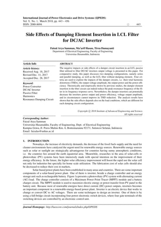
  • 1. International Journal of Power Electronics and Drive Systems (IJPEDS) Vol. 9, No. 1, March 2018, pp. 443 – 456 ISSN: 2088-8694 443 Institute of Advanced Engineering and Science Side Effects of Damping Element Insertion in LCL Filter for DC/AC Inverter Faizal Arya Samman, Ma’arif Hasan, Tirza Damayanti Department of Electrical Engineering, Faculty of Engineering Universitas Hasanuddin, Indonesia Article Info Article history: Received Aug. 18, 2017 Revised Dec. 11, 2017 Accepted Dec. 28, 2017 Keyword: Power Converter DC/AC Inverter Passive Filter Harmonics Resonance Damping Circuit ABSTRACT The negative impacts or side effects of a damper circuit insertion in an LCL passive filter utilized to filter DC/AC inverters output voltage is presented in this paper. For comparative study, this paper discusses two damping configurations, namely series and parallel damping, as well as the LCL filter without damping element. Four cri- teria are used to explore the impacts of the damper circuits, i.e. their total harmonic distortions (THDs), the output voltage amplitude, the output power and the power effi- ciency. Theoretically and empirically shown by previous studies, the damper element insertion in the filter circuit can indeed reduce the peak resonance frequency of the fil- ter in its frequency response curve. Nevertheless, the damper insertion can potentially decrease the inverters power output and power efficiency, voltage output amplitude, and in circumstances cannot improve its THD reduction. The analysis results have shown that the side effects depends also on the load conditions, which are different for each damping circuit configuration. Copyright c 2018 Institute of Advanced Engineering and Science. All rights reserved. Corresponding Author: Faizal Arya Samman Universitas Hasanuddin, Faculty of Engineering, Dept. of Electrical Engineering Kampus Gowa, Jl. Poros Malino Km. 6, Bontomarannu 92171, Sulawesi Selatan, Indonesia Email: faizalas@unhas.ac.id 1. INTRODUCTION Nowadays, the increase of electricity demands, the decrease of the fossil fuels supply and the need for cleaner environments have catalyzed the urgent need for renewable energy sources. Renewable energy sources such as solar or sunlight are strategically advantageous for countries having sunny atmospheric conditions, i.e. the countries lies around the earth equatorial area. Meanwhile, researches in the area of solar-cells or photovoltaic (PV) systems have been intensively made with special intention on the improvement of their energy efficiency. In the future, the higher solar efficiency improvement will boost the rapid use the solar cell not only for industries but specially for home scale utilization. The fabrication cost of solar cells should also be decreased to reduce their cost in markets. Solar-based power plants have been established in many areas and countries. There are some important components of a solar-based power plant. One of them is inverter, beside a charge controller and an energy storage unit such as rechargeable battery. Figure 1a presents a photovoltaic (PV) system with alternating current (AC) load. The charge controller consists of a Maximum Power Point Tracer (MPPT) module and a battery charger circuit. The MPPT module is used to maximize electric energy or power transfer from PV panel to the battery unit. Because most of renewable energies have direct current (DC) power outputs, inverters becomes an important component in a renewable-energy-based power plant. Inverter is an electric device that works to change or convert DC to AC voltages. There are some techniques to design an inverter. One of them is by using a full-bridge circuit incorporating four power electronic switch devices, where four gate terminals of the switching devices are controlled by an electronic control unit. Journal Homepage: http://iaescore.com/journals/index.php/IJPEDS Institute of Advanced Engineering and Science w w w . i a e s j o u r n a l . c o m , DOI: 10.11591/ijpeds.v9.i1.pp443-456
  • 2. 444 ISSN: 2088-8694 MPPT Module Battery Charger Battery Unit DC/AC Inverter + Filter Load 220V/ 50Hz/60Hz Solar Array VDC2 VDC3 VDC1 VAC VDC0 Charge Controller Unit Discussion Domain (a) Photovoltaic system Filter 9 10 17 7 1 2 4 V BATTERY M1 M2 M3 M4 5 3 7 8 6 0 NMOS Driver NMOS Driver NMOS Driver NMOS Driver Load Electronic Control Unit (ECU) D1 D2 D4 D3 C A A (b) inverter circuit topology Figure 1. The photovoltaic system and the DC/AC inverter and filter topology. There many challenging problems in designing an inverter. Some of them are summarized in the following items. • Power efficiency and switching loss due existing switching mechanism • Unbalance voltage due to unbalance loads in 3-phase inverter applications • Voltage amplitude and power factor shifting due to loading conditions • Grid synchronizations with an existing grid for hybrid power generation • Total harmonic distortion (THD) due to the used PWM-based switching mechanism to control the in- verter output Most of power losses in switched-mode inverter circuits are due to the existing switching mechanism. Switching pulses applied to the gate terminal of power switching devices will partially convert electrical energy to be thermal energy. Nowadays, new silicon technologies, such as Power MOSFET based on Silicon Carbide (SiC) technology can reduce power losses and have longer operating lifetime [1], [2]. Beside Power MOSFET, another switching device that can be used is Insulated Gate Bipolar Transistor or IGBT. Like power MOSFET, IJPEDS Vol. 9, No. 1, March 2018: 443 – 456
  • 3. IJPEDS ISSN: 2088-8694 445 the IGBT operations can also induce higher conductance losses and lower switching performance compared to SiC-based MOSFET [3]. The switching losses as well as electromagnetic interference can be avoid by a new concept i.e. by controlling the current and voltage slopes individually for all operating conditions of the IGBTs [4]. Voltage balancing is also a problem in inverter design especially in grid-connected applications. Stand- alone Micro Grid (MG) tends to have unbalancing voltage affected by the unbalanced load in single phase. To achieve the balancing of phase voltage, each single phase inverter can be controlled independently [5]. Other important aspects in inverter design are the output voltage amplitude, power efficiency and grid synchroniza- tion. Grid synchronization is especially very important in 3-phase grid-connected inverter applications [6]. The use of pulse width modulation (PWM) control systems, for instance in AC motor control appli- cations, causes the appearance of common mode voltage (CMV) at the neutral point. CMV suppression and elimination without influencing the inverter’s output voltage and better THD can be reached by using a special technique namely Partial elimination SVPWM (PE-SVPWM) and full elimination SVPWM (FE-SVPWM).[7]. The used of a coupled inductor multiplier can also reduce the conduction losses, due to the CMV at neutral point, and raise the efficiency [8]. Z-source T-type inverter is an example way to raise the efficiency system and to boost voltage level without any additional DC-DC converter or transformer. The method makes the output current of inverter are sinusoidal and synchronous with the grid frequency and its phase [9]. Leakage current is the drawbacks of grid-tied transformerless inverter systems. It produces system losses and inject harmonics into the grid [10], [11]. Therefore, the use of passive filter is important to imple- ment. The THD existence causes the inverter output voltage not be able to become pure sine wave as expected. To suppress the harmonic distortion, a passive filter is coupled to the output terminal of the inverter. According to the IEEE Standard, the acceptable THD of the inverter output voltage should be below 5% [12]. There are many filters that can be used to suppressed the THD, such as L, LC, LCL, LLCL, etc [13], [14], [15]. Among the aforementioned filters, the LCL filter has better capability to suppress harmonic distortion [16], [15]. Adding an LCL passive filter to the output terminal of an inverter can cause an appearance of peak resonance frequency. This phenomena can make the inverter system unstable and its performance becomes weak. Therefore, to suppress the resonance effect of the LCL passive filter, a resistance component as damper is inserted into the filter circuit. The resistance component inserted to the LCL passive filter is called as a resistance damping [17]. Multi-level inverters are also another type of inverter, which is proposed to reduce harmonics [18], [19] [20]. Multi-level inverter has multiple output voltage levels, which is enabled by the use of multiple DC source. In renewable energy applications, the design cost of a multi-level inverter is higher compared to a single-level inverter, due to the need for more DC/DC converters to maintain the voltage levels of the multiple DC sources. Single-level inverters are still favorable, since they are more simple with lower design cost. 2. RELATED WORKS AND CONTRIBUTION This paper will particularly discuss an LCL filter analysis. Since the use of LCL passive filter causes the appearance of resonant effect, a damping element is used. By using the damping element, the effect of resonant can be suppressed [17], [21]. However, the resonance damping resistor will raise an extra power loss, reduce maximum voltage amplitude and weaken the high-frequency harmonic reduction capability. This paper will show a comparative study on a few filter circuit with and without damping element. The LCL passive filter with and without the resistance damping tested with resistance loads. The criteria used in this study are the capability of LCL passive filter with and without resistance damping in reducing the harmonic distortion, maintaining the maximum output voltage amplitude and average output power as well as the power efficiency of inverters and filters. To the best of the author’s knowledge, the study of this paper, which is based on concurrent analysis of those four criteria with variable (resistance) loads, has not been explored by the previous works. The work in [17], for example, investigates many filters with active and passive damping methods. The work in [22] proposes different passive damping tuning methods and its analytical damping losses estimation. Nevertheless, both do not expose the impact of the resonance damping element insertion for different load conditions with extra side effects analysis on the THD, power output, power efficiency and the output voltage amplitudes. Variable loading conditions should be taken into account, since in practical conditions, the load is unknown and can potentially affect the load voltage and load current variables. Moreover, the load can be topologically Side Effects of Damping Element Insertion in LCL ... (Faizal Arya Samman)
  • 4. 446 ISSN: 2088-8694 involved as the part of the filter. 3. RESEARCH METHOD To achieve the research objective, systematical steps are used to explore the filter and inverter circuit characteristics. The filter and inverter are modeled in (Simulation Program with Integrated Circuit Emphasis). The transfer function of the filter is also mathematically modeled and then numerically modeled to obtain the frequency response curves. By using a SPICE simulator, the inverter+filter circuits are simulated for different load impedance values to measure some parameters and variables, i.e. 1. The THD or total harmonic distortion of the filter output voltages. The analysis is made for 100 harmonic frequency values, where 50 Hz is set as the base frequency. 2. The voltage amplitude values at the inverter’s input and output terminals, as well as at the filter output terminal. 3. The average output powers at the inverter’s input and output terminals, as well as at the filter output terminal. 4. The power efficiency of the inverter output power over the inverter input power, the filter output power over the inverter output power, and the efficiency of the filter output power over the inverter input power. After collecting the simulation data, the characteristic curves of all four aforementioned simulation parameters relative to the changes of load impedance values are plotted, and then some concluding remarks are given. 4. FILTER MODELING AND ANALYSIS The simulated inverter and filter circuit is presentedg in Figure 1b. The inverter as well as the filter circuit is modelled in SPICE. The electronic control unit (ECU) as shown in the figure generates four sinusoidal pulse width modulation (SPWM) signals. The voltage level of the SPWM signals is amplified using NMOS gate driver such that it can drive the n-channel power MOSFET at the points 3, 5 , 6 and 8, respectively as shown in Figure 1b. Each two of the SPWM signals has similar phase and waveform. The waveform of SPWM signals at the points 3 and 8 is similar, while the other one at the points 5 and 6 is also similar. The NMOS driver increases the voltage level to effectively drive the NMOS gate terminal. In general this driver separates optically the power converter circuit (having higher power) with the electronic control unit (having lower power), or is used to protect the ECU from the higher power circuit. In order to generate a sine waveform from the output terminal of the inverter, we need to generate some signals to control the process. Normally, this process is made under control of the ECU. The ECU should be programmed to generate two sine-based pulse width modulation (SPWM) as presented by the curves at the second and third line plots in Figure 2. In order to generate the SPWM signals, there are some techniques that can be used. One of them is illustrated from the curves at the first line plot in the Figure 2. An absolute sine wave, called as modulating signal (Vmod), is generated having 50 Hz frequency, as well as a carrier signal (Vcarr) in sawtooth waveform. The figure presents the carrier signal with 20 sawteeth in every half period of the sine wave signal. Both signal are compared each other to generate the SPWM using the following rule. When Vcarr > Vmod then Vgate = 0, else Vgate = 5 V . We assume that the logic ’1’, generated by the ECU, is related to 5 V. During the first half period of the sine wave signal, the SPWM signal is applied to the gates of MOSFET M1 and M4. Then, during the next second half period, the SPWM signal is applied to the gates of MOSFET M2 and M3. Consecutively applying this periodic waveform to the MOSFET gate terminals, then we will have the inverter’s output voltage as shown in the fourth line plot in the Figure 2. It seems that the inverter generates AC signal but with large total harmonic distortion (THD). Because, the output voltage of the inverter contains the THD value larger than 5%, then a filter circuit is required to decrease the THD below 5%. There many types of filters that can be used to suppress the THD. In general, the filter can classified as active and passive filters. Active filters are rarely used due to the complexity of circuit, especially for high power applications. Passive filters are mostly used in industries because of their IJPEDS Vol. 9, No. 1, March 2018: 443 – 456
  • 5. IJPEDS ISSN: 2088-8694 447 0 0.005 0.01 0.015 0.02 0.025 0 0.5 1 Inverter Output without Filter (20 sawteeth per half period) Vcarr Vmod (V) Carrier Voltage Modulator Voltage 0 0.005 0.01 0.015 0.02 0.025 0 2 4 6 Vgate1,4 (V) 0 0.005 0.01 0.015 0.02 0.025 0 2 4 6 Vgate2,3 (V) 0 0.005 0.01 0.015 0.02 0.025 −20 0 20 Inv. Vout (V) Time (second) Figure 2. The inverter output signal generation without filter by using 20 sawteeth per half period (The THD of the inverter’s output voltage is 47.829%). simple use and low cost utilization. the discussion about the used filters to suppress the THD is presented in the following sub section. Rds L1 C L2 ZL Filter + series damper Load Vin Vout (b) L1 C L2 ZL Filter without damper Load Vin Vout (a) Rdp L1 C L2 ZL Filter + par. damper Load Vin Vout (c) Vd Vd Vd Figure 3. The circuit configuration of the filters under evaluation: (a) filter without damping, (b)(c) filters with passive series and parallel damping methods [17]. 4.1. Filter Model without Damper The filter model without a damper element is presented in Figure 3(a). The transfer function of the Vout(s) Vd(s) is as follows. Side Effects of Damping Element Insertion in LCL ... (Faizal Arya Samman)
  • 6. 448 ISSN: 2088-8694 Vout(s) Vd(s) = ZL sL2 + ZL (1) The transfer function of the Vd(s) Vin(s) is as follows. Vd(s) Vin(s) = 1 s2L1C + 1 (2) By using the Laplace Transform Characteristic, the transfer function of Vout(s) Vin(s) can be obtained by multiplying Eq. (1) and Eq. (2), which results in the following equation. Vout(s) Vin(s) = ZL sL2 + ZL 1 s2L1C + 1 (3) Simplifying Eq. (3), we will have the final transfer function form, i.e. Vout(s) Vin(s) = ZL s3L1L2C + s2ZLL1C + sL2 + ZL (4) 4.2. Filter Model with Series Damper The filter model with a damper element inserted in series with the C-element of the filter is presented in Figure 3(b). Zds is obtained by deriving the equivalent impedance between the C-element and the series resistant damper Rds, i.e. Zds = Rds + 1 sC = sRdsC + 1 sC (5) The transfer function of the Vout(s) Vd(s) is the same result presented in Eq. (1). The transfer function of the Vd(s) Vin(s) is as follows. Vd(s) Vin(s) = Zds sL1 + Zds = sRdsC + 1 s2L1C + sRdsC + 1 (6) By using the Laplace Transform Characteristic, the transfer function of Vout(s) Vin(s) can be obtained by multiplying Eq. (1) and Eq. (6), which results in the following equation. Vout(s) Vin(s) = ZL sL2 + ZL sRdsC + 1 s2L1C + sRdsC + 1 (7) Simplifying Eq. (7), we will have the final transfer function form, i.e. Vout(s) Vin(s) = sZLRdsC + ZL s3L1L2C + s2(ZLL1C + RdsL2C) + s(L2 + ZLRdsC) + ZL (8) 4.3. Filter Model with Parallel Damper The filter model with a damper element inserted in parallel with the C-element of the filter is presented in Figure 3(c). Zdp is obtained by deriving the equivalent impedance between the C-element and the series resistant damper Rdp, i.e. Zds = Rdp 1 sC Rdp + 1 sC = Rdp sRdpC + 1 (9) The transfer function of the Vout(s) Vd(s) is the same result presented in Eq. (1). The transfer function of the Vd(s) Vin(s) is as follows. IJPEDS Vol. 9, No. 1, March 2018: 443 – 456
  • 7. IJPEDS ISSN: 2088-8694 449 Vd(s) Vin(s) = Zdp sL1 + Zdp = Rdp s2RdpL1C + sL1 + Rdp (10) By using the Laplace Transform Characteristic, the transfer function of Vout(s) Vin(s) can be obtained by multiplying Eq. (1) and Eq. (10), which results in the following equation. Vout(s) Vin(s) = ZL sL2 + ZL Rdp s2RdpL1C + sL1 + Rdp (11) Simplifying Eq. (11), we will have the final transfer function form, i.e. Vout(s) Vin(s) = ZLRdp s3RdpL1L2C + s2(L1L2 + ZLRdpL1C) + s(ZLL1 + RdpL2) + ZLRdp (12) 4.4. Frequency Response Characteristic After obtaining the transfer function of the filter circuits with three different damping element con- figuration, including the one without damping element, then this subsection presents the frequency response characteristic of the filters. Figure 4 presents the bode plot comparison of the filter circuits. 10 2 10 3 −20 0 20 40 60 Freq. Response of the Filters (Rds=3 Ohm, Rdp=300 Ohm) Frequency (rad/s) Magnitude 10 2 10 3 −200 −100 0 100 200 Frequency (rad/s) Phase (deg.) no damp. series damp. parallel damp. Figure 4. The transfer function of the filter with and without damping. 5. SIMULATION RESULTS AND ANALYSIS The steady-state and transient analysis or simulation results of some important measured variables in the inverter plus filter configurations are presented in this section. the simulations are made using SPICE Side Effects of Damping Element Insertion in LCL ... (Faizal Arya Samman)
  • 8. 450 ISSN: 2088-8694 (Simulation Program with Integrated Circuit Emphasis), which is an industry standard circuit simulator. The measured parameters are inverter’s and filter’s output voltages, output currents, output powers including the average output powers. The THD and power efficiency measurements of the inverter and filter circuit are also made in the analysis. 5.1. Steady-State Point Analysis In this steady state point analysis or simulation, the measured parameters are THD, voltage and current amplitudes, output power and power efficiencies. In every simulation run, the circuit is simulated until the steady-state condition is attained, and then, the parameters are observed from the SPICE output probe windows. The simulation results are shown in the following sub sections. 5.1.1. THD and Voltage Amplitude Measurements The upper section of Figure 5 shows the THD measurements at the filter’s output points. Each fig- ure presents three THD curves comparisons between the inverter+filter circuits without damping, with series damping and with parallel damping for different resistance loads, i.e. from 100 Ω until 105 Ω. As shown in the figure, the filter without damping element presents the best THD values, when the load impedance is above 20 Ω. Below that impedance value, the filters with damping elements have better THD values, but all of them have THD above 5%, the standardized THD limit. 10 0 10 1 10 2 10 3 10 4 10 5 0 5 10 15 20 Resistive Load (Ohm) THD (%) THD Curves, Inverter and Filter Output Voltages 10 0 10 1 10 2 10 3 10 4 10 5 26 Inverter Vout (V) 10 0 10 1 10 2 10 3 10 4 10 5 0 100 200 300 Resistive Load (Ohm) Filter Vout (V) LCL without Damping LCL with Series Damping LCL with Parallel Damping Figure 5. The THD measurements. The middle and lower sections of Figure 5 shows the voltage amplitude measurements at the inverter’s and filter’s output points. Each figure presents the curves comparisons between the inverter+filter circuits without damping, with series damping and with parallel damping for different resistance loads, i.e. from 100 Ω until 105 Ω. The voltage measurements at the inverter’s input terminal are not presented, since they present equal value, i.e. 24 V for each aforementioned resistance load value. IJPEDS Vol. 9, No. 1, March 2018: 443 – 456
  • 9. IJPEDS ISSN: 2088-8694 451 The filter output voltage amplitudes of the circuit without damping element presents higher values compared to the filters with series and parallel damping element, especially for the load impedance above 10 Ω. For the load impedance below 10 Ω, all filter circuit presents almost the same results. 5.1.2. Current Measurements Figure 6 shows the current measurements at the inverter’s and filter’s input-output points. Each figure presents three current curves comparisons between the inverter+filter circuits without damping, with series damping and with parallel damping for different resistance loads, i.e. from 100 Ω until 105 Ω. At the upper part of the figure, the current measurements at the inverter’s input terminal are presented. At the middle part of the figure, the current measurements at the inverter’s output terminal are presented. At the bottom part of the figure, the current measurements at the filter’s output terminal are presented. 10 0 10 1 10 2 10 3 10 4 10 5 0 10 20 30 40 Inverter Iin (A) LCL without Damping LCL with Series Damping LCL with Parallel Damping 10 0 10 1 10 2 10 3 10 4 10 5 0 5 10 Inverter Iout (A) LCL without Damping LCL with Series Damping LCL with Parallel Damping 10 0 10 1 10 2 10 3 10 4 10 5 0 0.5 1 1.5 Resistive Load (Ohm) Filter Iout (A) LCL without Damping LCL with Series Damping LCL with Parallel Damping Figure 6. The current measurements. As shown in Figure 6, the circuit with series damping element has better inverter input currents com- pared to the circuit without damping element and the circuit with parallel damping element. For the load impedance above 50 Ω, the circuit without damping element has the best inverter output currents. The almost similar values are presented for the load impedance below 50 Ω. For the load impedance below 5kΩ, the output current of the filter without damping element has the highest current values. The almost similar filter output current are presented for the load impedance above 5kΩ. 5.1.3. Power Measurements Figure 7a shows the power measurements at the inverter’s and filter’s input-output points. Each figure presents three power curves comparisons between the inverter+filter circuits without damping, with series damping and with parallel damping for different resistance loads, i.e. from 100 Ω until 105 Ω. At the upper part of the figure, the power measurements at the inverter’s input terminal are presented. At the middle part of the figure, the curves present the power measurements at the inverter’s output terminal. At the bottom part of the figure, the power measurements at the filter’s output terminal are presented. Side Effects of Damping Element Insertion in LCL ... (Faizal Arya Samman)
  • 10. 452 ISSN: 2088-8694 10 0 10 1 10 2 10 3 10 4 10 5 0 20 40 60 Inverter Pin (W) LCL without Damping LCL with Series Damping LCL with Parallel Damping 10 0 10 1 10 2 10 3 10 4 10 5 0 10 20 30 Inverter Pout (W) LCL without Damping LCL with Series Damping LCL with Parallel Damping 10 0 10 1 10 2 10 3 10 4 10 5 0 10 20 30 Resistive Load (Ohm) Filter Pout (W) LCL without Damping LCL with Series Damping LCL with Parallel Damping (a) Power output measurements 10 0 10 1 10 2 10 3 10 4 10 5 0 50 100 Efficiency 1 (%) LCL without Damping LCL with Series Damping LCL with Parallel Damping 10 0 10 1 10 2 10 3 10 4 10 5 0 50 100 Efficiency 2 (%) LCL without Damping LCL with Series Damping LCL with Parallel Damping 10 0 10 1 10 2 10 3 10 4 10 5 0 50 100 Resistive Load (Ohm) Efficiency 3 (%) LCL without Damping LCL with Series Damping LCL with Parallel Damping (b) Power efficiency measurements Figure 7. The power output and power efficient measurements. The inverter input power values of the circuit without damping element are higher than the inverter input power of the circuit with damping elements for all load impedance value. For the load impedance below 2kΩ, the inverter output power values of the circuit without damping element are higher than the other config- urations. However, for the load impedance values above 2kΩ, the series damping element circuit configuration presents the highest inverter output power values. The filter without damping element has the higher output power compared to the other circuits with damping elements. 5.1.4. Power Efficiency Measurements The efficiency curves for the inverter and the filter are presented in Figure 7b. Each figure presents three efficiency curves comparisons between the inverter+filter circuits without damping, with series damping and with parallel damping for different resistance loads, i.e. from 100 Ω until 105 Ω. Efficiency 1 is the power efficiency of the inverter output power over the inverter input power, as presented in the upper part of the Figure 7b. In this case, the filters with damping elements have the highest power efficiency compared to the power efficiency of the filter without damping element for the load impedance values about 80 Ω. For the load impedance values below 80 Ω, power efficiency values of the circuit without damping element are almost the same as the values of the circuit with series damping element, but higher than the values of the circuit with parallel damping element. Efficiency 2 is the power efficiency of the filter output power over the inverter output power, as pre- sented in the middle part of the Figure 7b. In this case, the power efficiency of the circuit without damping element is higher than the circuits with series and parallel damping elements for all load impedance values. Efficiency 3 is the power efficiency of the filter output power over the inverter input power, as presented in the bottom part of the Figure 7b. In this case, the power efficiency of the circuit without damping element is higer than the circuits with series and damping elements. The highest power efficiency is shown to be around 10 until 100 Ω. 5.2. Transient Analysis In this subsection, the transient responses of the inverter’s output voltage, current, power and average power are presented. The transient responses for the three filter configuration, i.e. without damping, with parallel and series damping are presented and compared directly. Figure 8 shows the transient response curves, from upper until lower part of the figure, respectively for the output voltage the output current, output power and the average output power of the filter circuit without damper and with damper element. The load impedance is set to 500 Ω for both simulations. As presented in IJPEDS Vol. 9, No. 1, March 2018: 443 – 456
  • 11. IJPEDS ISSN: 2088-8694 453 0 0.05 0.1 0.15 0.2 0.25 0.3 0.35 0.4 −200 0 200 Vout (V) Time (second) 0 0.05 0.1 0.15 0.2 0.25 0.3 0.35 0.4 −0.5 0 0.5 Iout (A) Time (second) 0 0.05 0.1 0.15 0.2 0.25 0.3 0.35 0.4 0 20 40 60 Pout (W) Time (second) 0 0.05 0.1 0.15 0.2 0.25 0.3 0.35 0.4 0 10 20 Avg. Pout (W) Time (second) no damp. series damp. par. damp. Figure 8. Transient analysis of the filter’s output voltage and average power with and without damping with load impedance Zload = 500Ω. Figure 8, it seems that the filter without damping element has better voltage amplitude compared to the filters with the damper elements. The same result is presented for the average output powers. Compared to the parallel damped filter, the series damped filter shows better average power. 6. CONCLUSION AND OUTLOOKS This paper has presented the side effects of the damping element insertion in the passive LCL filters. Passive damping method with series configuration can indeed reduce peak resonance frequency. But, in case of higher damping resistor values, the insertion of a resistor in series with the capacitor in the LCL filter circuit as a damper element has disadvantages of decreasing the filter ability in eliminating its THD. It also decreases in the output voltage and reduces the average output power. The output voltage and the average power however can be still improved by choosing appropriate damping resistance values. In case of parallel damper element insertion in the filter with lower damping resistor values, the same drawbacks appear as same as the previous series damping configuration. It decreases the ability of the filter in reducing harmonics and drops the output voltage amplitude. The dropped output voltage depends on the resistance load value. The dropped voltage becomes larger as the resistance load is larger, but it tends to be steady for relatively larger resistance loads. Output voltage and average power, however, can be still improved by choosing appropriate damping resistance values. Larger resistance damper insertion can surely increase the power losses. In general, both damping methods (series and parallel damping) can indeed reduce resonance, in which the resonance effect can potentially reduce the filter system stability. However, based on this study, the methods should be applied carefully because it potentially gives negative impacts or side effects in terms of THD, the maximum output voltage (voltage amplitude), the inverters average output power and the power efficiency of the inverter and filter circuits. The impacts are also dependent on the resistance load values. Load conditions should be considered in the filter modeling, since the load can be topologically in- volved as the part of the filter. Unfortunately, in practical conditions, the load is unknown. But, theoretically, Side Effects of Damping Element Insertion in LCL ... (Faizal Arya Samman)
  • 12. 454 ISSN: 2088-8694 the load can be classified as pure resistance loads, loads causing leading current and loads causing lagging current. Hence, a filter that can be tuned over different load condition is required to maintain the inverter performance over the aforementioned criteria. ACKNOWLEDGEMENT The authors gratefully acknowledge the Ministry for Research, Technology and Higher Education of the Re- public of Indonesia for funding our research work under the scheme of “Post-Graduated Colleagium Research Grant” (Hibah Penelitian Tim Pasca Sarjana) with Grant Contract No. 005/SP2H/LT/DPRM/IV/2017 in the year 2017. REFERENCES [1] J. Biela, M. Schweizer, S. Waffler, and J. W. Kolar, “SiC versus Si Evaluation of Potentials for Perfor- mance Improvement of Inverter and DCDC Converter Systems by SiC Power Semiconductors,” IEEE Trans. on Industrial Electronics, vol. 58, no. 7, pp. 2872–2882, July 2011. [2] T. Ueda, “GaN, SIC Tout as Next Generation Power Switching Devices,” AEI Magazine, Tech-Focus, pp. 38–41, Nov. 2015. [3] G. Sena, R. Marani, G. Gelao, and A. G. Perri, “A Comparative Study of Power Semiconductor Devices for Industrial PWM Inverters,” International Journal of Power Electronics and Drive System (IJPEDS), vol. 7, no. 4, pp. 1420–1428, Dec. 2016. [4] Y. Lobsiger and J. W. Kolar, “Closed-Loop di/dt and dv/dt IGBT Gate Driver,” IEEE Trans. on Power Electronics, vol. 30, no. 6, pp. 3402–3417, June 2015. [5] R. M. Kamel, “New inverter control for balancing standalone micro-grid phase voltages: A review on MG power quality improvement,” Elsevier, Renewable and Sustainable Energy Reviews, vol. 63, pp. 520–532, Sept. 2016. [6] M. G. Villalva, T. de Siqueira, M. Espindola, and E. Ruppert, “Modeling And Control Of A Three-Phase Isolated Grid-Connected Converter For Photovoltaic Applications,” Revista Controle and Automacao, vol. 22, no. 3, pp. 215–228, May–June 2011. [7] C. Bharatiraja, S. Jeevananthan, J. Munda, and R. Latha, “Improved SVPWM vector selection approaches in OVM region to reduce common-mode voltage for three-level neutral point clamped inverter,” Elsevier, Electrical Power and Energy Systems, vol. 79, pp. 285–297, July 2016. [8] Y. Zhao, X. Xiang, C. Li, Y. Gu, W. Li, and X. He, “Single-Phase High Step-up Converter With Improved Multiplier Cell Suitable for Half-Bridge-Based PV Inverter System,” IEEE Trans. on Power Electronics, vol. 29, no. 6, pp. 2807–2816, June 2014. [9] S. Ozdemir, “Z-source T-type inverter for renewable energy systems with proportional resonant con- troller,” Elsevier, International Journal of Hydrogen Energy, vol. 10.1016/j.ijhydene.2016.01.140, no. article in press, pp. 1–12, 2016. [10] M. Azril and N. A. Rahim, “Design Analysis of Low-Pass Passive Filter In Single-Phase Grid-Connected Transformerless Inverter,” in Proc. of the IEEE First Conference On Clean Energy And Technology (CET), 2011, pp. 348–353. [11] B. Gu, J. Dominic, J.-S. Lai, C.-L. Chen, T. LaBella, and B. Chen, “High Reliability and Efficiency Single-Phase Transformerless Inverter for Grid-Connected Photovoltaic Systems,” IEEE Trans. on Power Electronics, vol. 28, no. 5, pp. 2235–2245, May 2013. [12] M. Hojabri and A.Toudeshki, “Third-Order Passive Filter Improvement for Renewable Energy Systems to Meet IEEE 519-1992 Standard Limits,” pp. 199–204, 2015. [13] M. Elsaharty and H. Ashour, “Passive L And LC Filter Design Method For Grid Connected Inverter,” in Proc. of the IEEE Innovative Smart Grid Technologies Asia (ISGT-ASIA), 2014, pp. 13–18. [14] W. Wu, Y. Sun, M. Huang, X. Wang, H. Wang, F. Blaabjerg, M. Liserre, and H. S.-H. Chung, “A Robust Passive Damping Method For LLCL-Filter-Based Grid-Tied Inverters To Minimize The Effect Of Grid Harmonic Voltages,” IEEE Trans. on Power Electronics, vol. 29, no. 7, pp. 3279–3289, July 2014. [15] F. A. Sammman and A. Azhari, “DC/AC Power Converter for Home Scale Electricity Systems Powered by Renewable Energy,” in Proc. of the 3rd IEEE Int’l Conf. on Smart Green Technology in Electrical and Information Systems (ICSGTEIS), 2016, pp. 149–154. IJPEDS Vol. 9, No. 1, March 2018: 443 – 456
  • 13. IJPEDS ISSN: 2088-8694 455 [16] W. Wu, Y. He, T. Tang, and F. Blaabjerg, “A New Design Method for the Passive Damped LCL- and LLCL-Filter Based Single-Phase Grid-tied Inverter,” IEEE Trans. on Industrial Electronics, vol. 60, no. 10, pp. 4339–4350, Oct. 2013. [17] M. Buyuk, A. Tan, M. Tumay, and K. Bayndr, “Topologies, Generalized Designs, Passive And Active Damping Methods of Switching Ripple Filters For Voltage Source Inverter: A Comprehensive Review,” Elsevier, Renewable and Sustainable Energy Reviews, vol. 62, pp. 46–69, Sept. 2016. [18] H. M. Bassi, “A Modulation Scheme for Floating Source Multilevel Inverter Topology with Increased Number of Output Levels,” International Journal of Electrical and Computer Engineering (IJECE), vol. 6, no. 5, pp. 1985–1993, Oct. 2016. [19] R. Benioub, L. Kadri, M. Adnane, and K. Itaka, “Modulation Index Variation Effect on Harmonic Behav- ior of Fifteen Multilevel Inverter Neutral-Point-Clamped Topology,” International Journal of Electrical and Computer Engineering (IJECE), vol. 7, no. 4, pp. 1892–1898, Aug. 2017. [20] N. H. Ramlan, N. A. Azli, and N. F. A. A. Hafidz, “Performance of Interconnection and Damping Assign- ment Passivity-Based Controller on Inverter Circuits,” International Journal of Power Electronics and Drive System (IJPEDS), vol. 8, no. 1, pp. 69–80, Mar. 2017. [21] J. Muhlethaler, M. Schweizer, R. Blattmann, J. W. Kolar, and A. Ecklebe, “Optimal design of LCL har- monic filters for three-phase PFC rectifiers,” IEEE Trans. on Power Electronics, vol. 28, no. 7, pp. 3114– 3125, July 2013. [22] R. Pena-Alzola, M. Liserre, F. Blaabjerg, R. Sebastian, J. Dannehl, and F. W. Fuchs, “Analysis of the Pas- sive Damping Losses in LCL-Filter-Based Grid Converters,” IEEE Trans. on Power Electronics, vol. 28, no. 6, pp. 2642–2646, June 2013. BIOGRAPHIES OF AUTHORS Faizal Arya Samman received his Bachelor of Engineering degree in Electrical Engineering (with honors) from Universitas Gadjah Mada (UGM), Yogyakarta in 1999 and his Master of Engineering degree from Institut Teknologi Bandung (ITB) in 2002. In 2002 he was appointed to be a research and teaching staff at Faculty of Engineering, Universitas Hasanuddin in Makassar, Indonesia. He re- ceived a scholarship award (2006–2010) from Deutscher Akademischer Austausch-Dienst (DAAD, German Academic Exchange Service) to pursue his Doktor-Ingenieur degree at Technische Uni- versität Darmstadt (TUD), Germany. From 2010 until 2012 he worked as the postdoctoral research fellow in LOEWE-Zentrum AdRIA (Adaptronik-Research, Innovation, Application) at Fraunhofer Institut LBF Darmstadt. His research interests include FPGA-based digital systems design, power electronics, network on-chip (NoC), systems-on-chip (SoC), and multi-core embedded computer systems. Ma’arif Hasan finished his Bachelor degree (with honors) in 2017 from Universitas Hasanuddin at Department of Electrical Engineering, with major study in the field of power system engineering. His research interests are power electronic converter and renewable energy systems. Side Effects of Damping Element Insertion in LCL ... (Faizal Arya Samman)
  • 14. 456 ISSN: 2088-8694 Tirza Damayanti finished her Bachelor degree (with honors) in 2017 from Universitas Hasanuddin at Department of Electrical Engineering, with major study in the field of telecommunication engi- neering. Her research interests are electric and electronic circuit analysis and filter circuit design. IJPEDS Vol. 9, No. 1, March 2018: 443 – 456