More Related Content
Similar to Surface_engineering_oppotunities2007
Similar to Surface_engineering_oppotunities2007 (20)
More from Boris Kobrin (14)
Surface_engineering_oppotunities2007
- 1. MICRONANOSYSTEMS 17
Surface engineering opportunities
Recent advances in nanotechnology have allowed companies to look at new techniques
when considering modification of surfaces through engineering. A number of potential
techniques are being explored. These emerging techniques are finding applications in
emerging technologies. Here Boris Kobrin of Applied Microstructures looks at the
growing opportunities for surface engineering.
October 2007 www.micronanosystems.info
Surface Engineering assumes modification of surface
properties of materials by means of application of
coatings or surface treatments. Recent advances in
nanotechnology opened an opportunity to modify surfaces in a
nanoscale range. Nanoscale surface engineering has found use in
many fields. It is driving miniaturisation of electronics and
medical devices, fabrication of new sensors and actuators as
well as in the creation of new classes of materials and devices.
A few years ago Molecular Vapour Deposition (MVDR)
technology was introduced to commercial markets by Applied
Microstructures as a surface engineering alternative to solution
based methods used in many laboratories for a last decade.
These methods include immersion of sample into a sequence of
solvent-based solutions. MVD technology, as a vapour based
technique, provides solvent-free, low material waste and a
environmentally friendly processing method. It also proved to
produce high quality nanocoatings due to its unique capability of
tightly controlling the process environment.
Nanocoatings, in the form of organic monolayer films, have
been commonly used to reduce the surface energy in
micro-structures to improve their performance and reliability.
Most notably, failures attributed to ‘release’ and ‘in-use’
stiction, which is the adhesion of compliant micromechanical
structure surfaces in close proximity, can be reduced by orders
of magnitude using a few angstrom-thick film. These anti-stiction
coatings are self-assembled monolayers (SAMs), which
can uniformly coat complex structures including high-aspect-ratio
comb drives in MEMS inertial sensors, areas under the
mirrors in MEMS displays, membranes of MEMS microphones,
and face plates of MEMS inkjet nozzles.
Stiction is a term that has been applied to the unintentional
adhesion of compliant microstructure surfaces when restoring
forces are unable to overcome interfacial forces such as
capillary, van der Waals and electrostatic attractions. The large
surface-area-to-volume ratios of surface and bulk
micromachined components bring the role of stiction into the
foreground, as adhesion of these microparts to
adjacent surfaces is a major failure mode for MEMS.
Conventionally, solution-based (wet processing) techniques
have been used to apply these films, however, the liquid
deposition process in manufacturing is extremely difficult to
apply due to particulation problems caused by the high
sensitivity of the reaction to environmental humidity.
Anti-stiction layers deposited from a vapor phase have proved to
enhance yield in MEMS devices by eliminating capillary stiction
phenomena, which in turn allows simplification and reduced cost
of MEMS packaging. Thin and conformal adhesion layers, in the
form of metal oxides, deposited in-situ prior to organic low
surface energy coatings, allow for the expanded range of useable
MEMS materials (metals, glasses and polymers) and provide
for enhanced mechanical, thermal and chemical stability.
Recently developments in MVD deposition technology has
transitioned from mainly R&D labs and pilot production into
high volume production facilities for the manufacturing of
MEMS displays, microphones and inkjet print heads.
Another exciting area of MVD surface engineering is
emerging technologies, and mainly Nanoimprint Lithography
(NIL). NIL is maturing as an alternative to optical lithography,
at least (and for now) in niche market applications, like hard
disk drives, LEDs, photonics, micro optics, and microfluidics.
Lux Research believes that nanoimprint tool business could grow
to nearly US$235 million by 2010.
One of the most promising areas of NIL is Data Storage,
where current technology approaches the magnetic media limit.
Conventional magnetic media consist of magnetic grains, each
one free to assume its own magnetisation state. The signal to
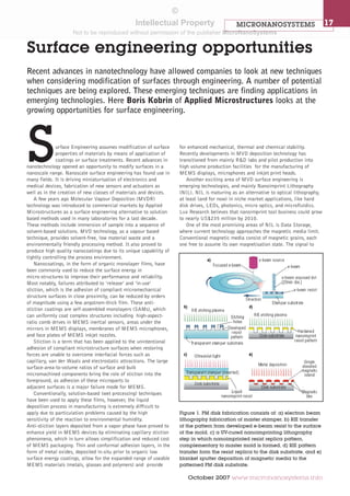
Figure 1. PM disk fabrication consists of: a) electron beam
lithography fabrication of master stamper, b) RIE transfer
of the pattern from developed e-beam resist to the surface
of the mold, c) a UV-cured nanoimprinting lithography
step in which nanoimprinted resist replica pattern,
complementary to master mold is formed, d) RIE pattern
transfer form the resist replica to the disk substrate, and e)
blanket sputter deposition of magnetic media to the
patterned PM disk substrate.
©
Intellectual Property
Not to be reproduced without permission of the publisher MicroNanoSystems
- 2. 18 MICRONANOSYSTEMS
noise ratio of the media is roughly proportional to the number of
magnetic grains per bit. The superparamagnetic limit is reached
at the point when grain becomes so small (<8 nm) that thermal
energy alone can flip its magnetisation direction. Today’s disk
drives have densities of 100 Gb/in2 with spacing of 86 nm.
Increasing capacity to 1Tb/in2 would require spacing of 27 nm,
and 10 Tb/in2 – 9 nm. For 500 Gb/in2 density and beyond
alternative to optical lithography technologies such as thermally
assisted recording (TAR) and patterned media (PM) are being
considered as likely routes.
Patterned Media (PM) has single-domain magnetic elements
having a uniform well-defined shape and specific location on a
disk. The PM master mold is fabricated using e-beam writing.
Then, the mold is used to replicate a pattern to a number of
individual disks. For example, one of the methods is in some
ways similar to the digital video disk (DVD) manufacturing
process (Fig 1), except that a UV-cured liquid resist is used
instead of relying on thermal softening of a solid polymer.
Another promising application of NIL, replication of micro
optics (diffractive optical elements, phase masks, Bragg
gratings, microlens arrays) has proved to be very useful in
driving down the cost of manufacturing optical components.
Microlenses and microlens arrays are finding applications
mainly in the domain of optical microsystems, including optical
interconnects, biomedical instruments, optical data storage and
optical communications. NIL techniques open a route for fast
and inexpensive prototyping of microlens arrays without
www.micronanosystems.info October 2007
compromising optical quality.
Another important potential application for NIL is
high-brightness LEDs, which are enhanced with photonic
crystals. A photonic crystal is a periodically repeating structure
made of two materials of different dielectric constants, which
can provide so called photonics band gap. As the dimensions of
2D photonic crystals are in the order of nanometers, NIL
nanolithography is an obvious choice.
NIL, as a printing technology, requires mechanical contact
between mould and resist (polymer material), thus resist
adhesion to the mould is one of the challenges for nanoimprint
lithography. When intimately contacted, resist tends to be pulled
from the substrate and remain on the mould. This creates a
defect, which affects not only the particulate substrate, but all
other consequently printed substrates because of an air gap
formed between a mold and a substrate. The main approach to
overcoming this problem it is to apply a low surface energy
coating to the mold surface, either in the solution phase or
vapour phase. Such low surface energy coating would
drastically reduce adhesive forces between mold and resist
materials.
The NIL replication process can be used for a fast fabrication
of plastic microfluidic devices. Large numbers of complex
microchannels are manufactured from a single master which
have been created using high precision optical or e-beam
lithography. This reduces the cost of such microfluidic device,
and hence allows the final device to be disposable.
Fig. 2. A schematic flow chart for replicating
microlenses in polycarbonate.
Fig. 3 LED device fabrication: a) Deposit Cr and PR; b)
Nanoimprint Process (50bar, 145C), c) Remove residual
area using O2 plasma, d) Etch the Cr and p-GaN region
Fig. 4. (a) FESEM Image of the LED sample after removal
of the residual layer and Cr Patterning, (b) Final PC
structures on a p-GaN layer
Fig. 5. Optical images (100x magnification) of portions of:
(a) a silicon oxide master for imprinting serpentine microfluidic
channel (b) the channels hot embossed in PMMA (c) a sectional
analysis of a PMMA channel (d) a SEM image of a channel in
PEN, nanoimprinted using the same master (bar=10 um).
©
Intellectual Property
Not to be reproduced without permission of the publisher MicroNanoSystems
- 3. MICRONANOSYSTEMS 19
October 2007 www.micronanosystems.info
Numerous coatings have been utilised as a low surface energy
release layer for NIL. Amorphous fluoropolymers, for example
Teflon AF, made by DuPond Fluoroproducts, Cytop,
manufactured by Asahi Glass, or Optool DSX of Daikin
Industries (20% solution in HFE) can be deposited by
spin-coating or dipping .
Unfortunately, deposition of these coatings in a liquid phase
into nm-feature structures is not always conformal, reproducible
or defect-free.
Self-assembled monolayers (SAMs) are considered an ideal
solution for NIL because of the self-assembling nature of these
films. The SAMs thickness is equal to the length of the molecule
of precursor use, thus thickness uniformity is excellent. SAMs
can be deposited from a liquid or vapour phase. Films deposited
from a vapour phase have fewer aggregates of the silane
molecules on the surface, because of vacuum process capability
to accurately controlling moisture environment. Moreover,
vapour is more effective than the solution in penetrating into the
nanoscale gaps of the mould, thus providing much lower defect
densities.
Applied Microstructures, Inc. offers equipment and
technology (Molecular Vapour deposition – MVDTM) for SAM
deposition from a vapour phase for variety of applications
including Nanoimprint Lithography. Fig. 8 shows simplified
schematics of the MVD-100 tool, which includes vacuum
chamber, integrated plasma source (for sample surface
pre-treatment with oxygen plasma), and three vapour delivery
lines configured for accurate delivery of reactive vapours.
Applied Microstructures first tool, the MVD-100 is a low
cost-solution for R&D and small production needs, while
MBD-150 tool, has capabilities to process an entire cassette
(25) of 8” wafers with an automatic loading and thus provides
capabilities for high-volume manufacturing.
In Fig. 10, a comparison of liquid and vapour deposited films
as measured by AFM are shown. In the micrographs, the z-scale
was 10nm. It can be observed that the liquid immersion film has
embedded particulates as shown in the red highlights, whereas
the MVD (vapour) deposited film was smooth and defect free.
The peaks in the thickness graphs were attributed to
particulation from excessive water. The uncontrolled source of
Fig. 6. Teflon AF (a) and Cytop (b) Release Layers structures
Fig. 7. Illustration of polymer, or resist, adhesion to mould
during mold release which causes pattern transfer deformation
and mould contamination (a), and a release layer to minimise
the adhesion to mould (b).
Fig. 8 .Schematics of MVD-100 tool for Release layers
deposition from a vapor phase
Fig. 9. R&D tool MVD-100 and Manufacturing tool MVD-150
Fig. 10. AFM images and scan plots of deposited SAM
comparing immersion and MVD process (Courtesy of AMO)
©
Intellectual Property
Not to be reproduced without permission of the publisher MicroNanoSystems
- 4. 20 MICRONANOSYSTEMS
water exists from ambient moisture. In contrast, particulates
can be eliminated in the MVD process by accurately controlling
the partial pressure of water which hydrolyses the precursor.
This results in improved pattern fidelity during imprinting.
The mould surface energy is greatly reduced as a result of the
formation of a densely packed perfluorinated monolayer which
reduces resist adhesion to the mould.
The surface coverage of the film is determined by measuring
the hydrophobicity against other published references.
Goniometric measurements (by a Ramé-Hart Inc.’s Advanced
Goniometer) show water static contact angles of ~110o and are
very repeatable from process run to run, as shown in Fig. 11.
On a smooth silicon surface, the high contact angles correlate to
a low surface energy of ~ 3μJ/m2 which is desirable for a good
release between the mold and resist. The SAM thickness
measurements performed with a Gaertner ellipsometer with at
an incidence angle of 70o @ 632.8nm. show an average
monolayer thickness of ~1.2 nm, which closely matches to the
thickness of a continuous molecular layer. Another advantage of
a vapour process for release layers is the high level of
conformality which can be achieved. The self-assembling and
self-limiting characteristics of the deposition process help to
maintain excellent critical dimension (CD) control of the mould
pattern. Therefore, a faithful replication of the mould pattern
can be generated in the resist. As shown in Fig. 12, CDs were
www.micronanosystems.info October 2007
measured on a CD SEM from feature of dense line in range
from 38 nm to 125 nm. The results show an excellent
correlation with no major deviations taking in account linewidth
and linewidth roughness.
For an imprint application, repeatability was evaluated by
monitoring mold release force and subsequent pattern inspection
of the pattern for more than 150 imprints. In Fig. 11, the
optical images of a patterned mould (right image) and without
(left image) of the MVD release layers are shown. The test trend
provides a good indication of the repeatability of the release
force required during the imprint process. With the vapour
deposited SAM release layer, the release force between the mold
and the resist was reduced to from over 20 to 15 Newtons
compared to uncoated moulds. The effectiveness of a MVD
release layer on mould release performance was also observed
by the mold pattern cleanliness. Excellent uniformity and
repeatability of the imprint critical features were achievable with
a MVD processed release layer.
Moulds made of Si or quartz materials are well suited as
stamps, particularly because the thermal expansion coefficient of
the stamp is often identical to the substrate to be structured.
Moreover, due to high density of natural bonding sites (hydroxyl
bonds) on Si and quartz surfaces silane based released layers can
form durable covalent bonding with the surface. For many NIL
schemes, however, other materials are used. For example, Ni is
widely used for industrial NIL applications, where higher level of
robustness is required. The most common surface of oxidised Ni is
the (100) surface of NiO, which is built up from Ni2+ cations and
O2- anions arranged in a sodium chloride structure. Due to the
highly ionic character of the Ni-O bonds the covalent linkage to
the silane group is chemically difficult. Moreover, the surface
state of the nickel is highly dependant on the plating process and
bath stock solution. Adhesion layers of SiO2 and TiO2, deposited
by e-beam evaporation, have been used to improve bonding of
silane-based release layers to Ni stamps.
Fig. 11. SAM release layer water contact angle monitoring for
process repeatability on silicon and on thick thermal oxide
Fig. 12. Linewidth correlation plot of CD measurement results
on template and imprinted resist for both ridges (diamonds) and
trenches (squares) (Courtesy of Quantiscript and EVG)
Fig. 13. Images of imprint mould and its release force graphs
with and without release layer (Courtesy of AMO GmbH)
©
Intellectual Property
Not to be reproduced without permission of the publisher MicroNanoSystems
- 5. MICRONANOSYSTEMS 21
October 2007 www.micronanosystems.info
Fig 14. clearly indicates that friction force of the release
layer depends on the underlying substrate surface. Silicon and
titanium oxide adhesion layers as thin as 5nm improve the
density of organic layers, which manifests itself in reduction of
surface energy. Recently, Applied Microstructures has widened
the range of materials which can be deposited using MVD
technology. For example, alumina (Al2O3) and titania (TiO2)
can now be deposited by MVD in-situ, without breaking a
vacuum in the same chamber, where organic release layers are
deposited. Thus, nanolaminates comprised of oxide adhesion
layers and organic low surface energy layer can be deposited in
a single automatic sequence.
For thermal embossing of NIL, the thermal stability of
release layers is very important. Coatings should withstand high
temperatures (150-400 C) and considerable pressures (up to
100 lb/cm2). It was demonstrated that MVD engineered
nanolaminates, comprised of oxide adhesion layers and organic
release layers provide necessary thermal stability, as show on
Fig 15.
Fig. 15.
Thermal
treatment
stability of
MVD Organic
Release layers
(FDTS) with
oxide
adhesion
layers
deposited
in-situ.
Durability of the coatings against mechanical impact was
estimated using IPA wipe tests, as shown on Fig 16. Coatings on
both, Si and Ni substrate materials show good stability for up to
40 wiping cycles.
Fig. 16. IPA
wiping
stability of
MVD Organic
Release
layers
(FDTS) with
oxide
adhesion
layers
deposited
in-situ.
Conclusions:
We believe that Nanoimprint Lithography (NIL) can
be an invaluable manufacturing solution for a number
of emerging technology applications including data
storage, optics and microfluidics. These applications
usually do not require stringent alignment and overlay
registration, which continue to be a considerable
challenge for NIL.
Moreover, NIL has proven to be the only
cost-effective solution for the creation of sub-100nm
feature devices, which makes it an obvious choice for
high volume low cost applications including data
storage, disposable lab-on-a-chip devices, and micro
optics.
The technological challenges of minimising defects
associated with the withdrawing the imprint mold from
the substrate material that it has imprinted can be
effectively overcome by the application of low surface
energy release layers to the mold prior to the
imprinting process.
MVDR (Molecular Vapour Deposition) technology
provides a convenient and
cost-effective way to apply these extremely thin and
durable layers in a vapour phase.
The combination of organic layer deposition with
inorganic adhesion layers deposited in-situ allows
implementing this technology to a wider range of
mold/stamp materials.
Therefore, NIL systems implemented with MVD and
its associated unique characteristics can produce parts
with uniform, exact and repeatable surfaces resulting
in a highly enhanced yielding process. Since its recent
introduction in 2004, MVD technology has been widely
adopted into high volume manufacturing of MEMS
displays, inkjet nozzles and microphones.
MVD tools are currently used extensively in
nanoimprint technology development in many
universities and nanofabrication facilities around the
globe and it will surely play an important role in NIL’s
transition from development to high volume
manufacturing stage in many additional applications.
Fig. 14. Friction vs. normal force curve measured by LFM for
TFS coatings on Ni with oxide adhesion layers and Surface
energy for a dual layers of TFS/SiO2 on Ni
Fig 17 AFM scans of NIL structures, 50nm linewidth (a) and
70nm linedwidth (b), release with MVD layers. Not rectangular
profile of the structures associated with limited size of AFM tip.
(Courtesy of Suss Microtech)
©
Intellectual Property
Not to be reproduced without permission of the publisher MicroNanoSystems