SlideShare a Scribd company logo
1 of 51
Digital System Design
Introduction
Digital System
• A digital signal is discrete-time
as well as discrete-valued signal
• A system that works with digital
signal is digital system
• Digital doesn’t always mean
binary
Why Digital?
• Perfect
Reconstruction/Regeneration
• Error control (ARQ / FCS)
• Encryption/Decryption
Advantages of Digital
System
• Easy to store and retrieve digital
information
• Easy to process digital data
• Digital is less error prone
• Error can be controlled
• Noise does not accumulate from
one logic stage to next as it does
in analog system (Regeneration)
• The ease of large scale
fabrication
• Can be processed by a general
purpose processor
Analog vs. Digital
design
• Digital design need to handle
with only few specified (mostly
two) logic levels
– It is less important to precisely
simulate resistive,
capacitive and inductive parameters
– Design simulation can be based on
the logic only,
tools can therefore follow the truth
tables
Analog vs. Digital
design
• Analog design requires precise
voltage and current
characteristics of the devices
– Parasitic capacitance, resistance,
inductance are
very important – Circuit elements are
non-linear – Design verifications
require complex simulations
involving solutions of differential
equations
Integrated Circuits
Integrated Circuit (IC)
• A set of electronic circuits on one
small plate ("chip") of semiconductor
material, usually silicon
• Much smaller than a discrete circuit
made from independent electronic
components
• ICs can be made very compact,
having up to several billion
transistors and other electronic
components in a very small area
• The width of each conducting line in
a circuit is being smaller and smaller
as the technology advances (from
micrometer to nanometer)
• In 2008 it was dropped below 100
nanometers, and has now been
reduced to tens of nanometers
Why ICs
• Let a recent PC is more than
1000 times faster than that in
1982 then:
– If one small table was required to
set a PC in 1982,
now does it requires more than 1000
tables to set a PC? – If a PC in 1982
consumed one unit of power, now
does it need to supply more than
1000 unit of power?
Why ICs
• 80286 microprocessor
– released on February 1982 – with
134,000 number of transistors
• Pentium Pro microprocessor –
released on November 1995 – with
5,500,000 number of transistors
Why ICs
• Electronic systems are
backbone of many systems
today, and it is a continuous
trend towards digital
electronics solutions in all
areas of our life – Car electronics
which includes music system, engine
and dashboard controls –
Electronics in aircraft, Washing
Machines, Computing and
Computers etc. – Communication,
Phones, entertainment, TVs,
measurements (instrumentation)
etc.
Properties of IC
• Size:
– Integrated circuits are much
smaller, both
transistors and wires are shrink to
micrometer (or even nanometer)
sizes within IC – Smaller size leads
to advantages in speed and
power consumption, because smaller
components have smaller parasitic
capacitances, resistances
Properties of IC
• Speed: – Signals can be switched
between logic 0 and logic1 much
quicker within a chip –
Communications within a chip can
occur hundreds of times faster than
communication between chips –
The high speed within chip is
possible due to their small size. The
smaller components and wires
have smaller parasitic
capacitances to slow down the
signal
Properties of IC
• Power consumption:
– Logic operations within a chip takes
much less
power – Due to small size of circuits
on the chip-smaller parasitic
capacitances and resistances
requires less power to drive them
Advantages of ICs
• Small physical size
• High speed
• Low power consumption
• Reduced cost
• High reliability
• Good performance
Properties of Digital
Circuits
Properties of Digital
Circuits
• The binary output signal must
be a prescribed function of the
binary input or inputs
• Quantization of amplitudes
within the normal range of
operating voltage is required,
which implies strong
nonlinearities in circuit operation
Properties of Digital
Circuits
• Amplitude levels are
regenerated in passing from the
input to the output of a digital
circuit
• Changes in an output level
should not appear at any
unchanging input of the same
circuit; there must be an explicit,
unilateral cause- effect
relationship between input(s) and
output(s)
Properties of Digital
Circuits
• The output of one circuit must
be capable of driving more than
one input of similar circuits
• The number that can be driven
is termed as fan-out of the
circuit
• The digital circuits must be
capable of accepting more than
one input, the number of
independent input nodes is
termed as fan-in
Modern Electronics
Development
Modern Electronics
Development
• The invention of transistor at Bell
Telephone Laboratories in 1947
• The introduction of bipolar transistor
by Schockley in 1949
• 1956 the first bipolar digital logic
gate by Harris
• The first truly successful IC logic
family, TTL (transistor transistor
logic) was pioneered in 1962
• Other logic families were devised
for higher performance i.e. ECL
(emitter coupled logic) – first
subnanosecond digital gates
Modern Electronics
Development
• TTL had the advantage of offering
higher integration density and was
the basis of first integrated circuit
revolution
• Ultimately, in bipolar digital logic,
the large power consumption per
gate puts an upper limit on the
number of gates that can be
reliably integrated on a single die
or package
• The attempts were made to develop
high integration density, low-power
bipolar families (such as I2L –
Integrated Injection Logic)
Modern Electronics
Development
• The torch was gradually passed
to the MOS digital integrated
circuit approach
• The basic principle behind the
MOSFET transistor was
proposed in a patent by J.
Lilienfeld (Canada) as early as
1925, and independently by
O. Heil in England in 1935
• Insufficient knowledge of
materials and gate stability
problems delayed the practical
usability of the device for long
time
Modern Electronics
Development
• The next age of the digital
integrated circuit revolution was
inaugurated with the introduction of
the first microprocessors by Intel in
1972 the 4004 and in 1974 the 8080
• MOS technology enabled the
realization of the first high-density
semiconductor memories
• The large majority of the current
integrated circuits are implemented in
the MOS technology
Moore’s Law
• Gordon Moore: co-founder of Intel
• In 1960, he predicted that number
of transistors per chip would grow
exponentially (double every 18
months)
• This prediction later called Moore’s
law, has proven to be amazingly
visionary
• Integration complexity doubles
approximately every 1 to 2 years, as
a result, memory density has
increased by more than a
thousand-fold since 1970
Evolution in
Complexity
Evolution in
Transistor Count
Evolution in
Speed/Performance
10 μm – 1971 6 μm –
1974 3 μm – 1977 1.5 μm
– 1982 1 μm – 1985 800
nm – 1989 600 nm –
1994 350 nm – 1995 250
nm – 1997 180 nm –
1999
130 nm – 2001 90 nm –
2004 65 nm – 2006 45
nm – 2008 32 nm – 2010
22 nm – 2012 14 nm –
2014 10 nm – 2016–2017
7 nm – 2017–2018 5 nm
– 2020–2021
Hierarchical Design
• Divide and conquer approach
• Design complexity is reduced
by breaking it down into
manageable pieces
• Example: – A 32 bit ripple carry
counter design is specified as 32 flip
flops – Each flip flop is specified as
connection of several gates – Each
gate as connection of transistors
Design Abstraction
• Multiple levels of design
abstraction are given for the ICs
• Design abstraction goes from
the specifications to layout (or
the physical design)
Design Abstraction for
the ICs
Specifications
Behavior
RTL specs
Logic
Circuit
Layout Natural language
Complexity HDL
Finite State Machine
List of gates
Abstraction
Transistor level circuit
With EDA tools, design abstraction
can be high Physical realization
and lower level can be synthesized
Design Abstraction
Levels
MODULE
+
GATE
CIRCUIT
DEVICE
G
S
n+ n+
SYSTEM
D
Design Techniques
• Two contradicting issues
– increasing complexity of the
designs – reducing time for design
• Only possible solutions are
– increase more and more
automation – multiple levels of
abstraction for design to eliminate
unnecessary details
Electronic Design
Automation (EDA)
Electronic Design
Automation (EDA)
• Automation of the Electronic
Design
• A category of software tools for
designing electronic systems
i.e. printed circuit boards and
integrated circuits
• The tools work together in a
design flow that chip designers
use to design and analyze
entire semiconductor chips
• Also referred to as "Electronic
Computer- Aided Design"
(ECAD)
EDA
• Transistor simulation: low-level
transistor- simulation of a
schematic/layout's behavior at
device-level
• Logic simulation: digital-
simulation of an RTL or gate's
digital (Boolean 0/1) behavior, at
Boolean-level
• Behavioral Simulation: high-
level simulation of a design's
architectural operation
EDA
• Issues
– Devices: transistors, gates, flip
flops, digital building blocks, memory,
processors etc. – Levels: Chip,
Board, System, Concept – Simplicity:
Custom Design vs. reuse of design
• EDA focus is mainly on digital
circuit design though analog is
getting in
EDA
• With high speed designs,
various other issues are also
important – Interconnect resistance
and capacitance – RF interference,
induced currents etc.
• EDA need to take care of this
using various simulation
• Before EDA, integrated circuits
were designed by hand, and
manually laid out – time
consuming and difficult
EDA Examples
• EAGLE for PCB Design by
CadSoft Computer
• National Instruments
Electronics Workbench Group
– NI Multisim - schematic capture
and simulation – NI Ultiboard -
printed circuit board layout editor
• Advanced Design System for
high frequency and high speed
design by Keysight Technologies
Digital System and
Characteristics
Requirements
• Highly reliable
• Low power consumption
• Small size
• High speed
• Low cost and
• High performance
But there is trade-offs between requirements
Choices
• Logic family
– What are the permissible tradeoffs ?
• Level of integration
– How many functions?
• Programmable versus fixed
function circuits
– What is the context?
Logic families
• Various logic families are:
– Diode Logic – Diode Transistor
Logic (DTL) – Resistor Transistor
Logic (RTL) – Transistor Transistor
Logic (TTL) – Emitter coupled logic
(ECL) – Integrated Injection Logic
(I2L) – MOS:- NMOS, PMOS and
CMOS
Level of integration
• Small-scale integration (SSI):
no of gates less than 10
– Simple logic functions, basic storage
elements etc.
• Medium-scale integration
(MSI): 10–100 gates
– 4-bit adders, 8-to-1 multiplexers,
counters, etc.
• Large-scale integration (LSI): 100 to a
few 1000 gates
– Programmable logic array (PLA), PROM,
small processors, etc.
• Very large-scale integration (VLSI):
several thousand to millions of gates
– Processors, large memory array, etc.
• Ultra large-scale integration (ULSI): no of
gates > 10 million
– Advanced processors, system chips, etc.
An ideal logic element
• Operates from a single power
source
• Draws a minimum of power, ideally
zero
• The two binary output levels are 0
and vDD
Vcc
inputs
output
Gnd Out
VDD
VDD/2 In
contd...
• The output impedance is low, so
that large current may be
delivered to external loads
without altering the output
voltage levels
• The transition between states
at output occurs abruptly for an
input level equal to one half the
supply voltage
contd...
• There is no time delay between
the input transition and the
consequent output transition
• Virtually any numbers of inputs
are available; the input
impedance is high so that the
circuit imposes little loading on
the driving signal
Noise and noise margin
• Noise:-
– Any unwanted signal added to vary
voltage or
currents at logic nodes – If the
magnitude of noise is high it will cause
logic
errors
contd...
• Noise margin:-
– The maximum noise voltage level
that a logic
signal can tolerate without any error –
If the noise amplitude at input at any
logic is
smaller than noise margin (a specified
critical magnitude) the noise
amplitude will be attenuated – High-
level noise margin: NMH=VOH - VIH –
Low-level noise margin: NML=VIL -
VOL
Vcc(5 V)
Vec(5 V)
H
VOH (2.4)
High noise
margin
VIH (2.0)
VIL (0.8)
VOL (0.4)
Low noise margin
GND (0)
GND (0)
Output voltage
range
Input voltage
range
Mutual inductance with another logic node
--Inductive and
resistive drops
-Capacitive coupling from another node
3
Radio frequency signals from external sources
Transient
characteristics
• Rise time – Time taken by the
signal to switch from 10% to 90% of
its normal value
• Fall time – Time taken by the
signal to switch from 90% to 10% of
its normal value
• High-low and low-high
transition times at the output of
a gate are defined as tHL and
tLH
Transient
characteristics
• Propagation delay
– It takes certain amount of time to
propagate from
input to the output – Propagation
delay is the average transition delay
for a signal to propagate from input to
output when the binary signals
change in value – tPHL, tPLH and tPD
• tPHL:- the time required for the
output signal to reach 50% of
its normal value on the H-to-L
transition after the input signal
reached 50% of its normal
signal • tPLH:- the time required
for the output signal to reach
50% of its normal value on the
L-to-H transition after the input
signal reached 50% of its
normal signal • tPD:- It is the
mean of the above two and is
generally used for hand
calculations. And in early days
max of the two quantities was
considered
Propagation delay for
an Inverter
High-to-low (tPHL) and low-to-high (tPLH) propagation
delays are measured on output transitions
Power
• Power supply (VCC)
– Power required by the circuit to
operate
• Power dissipation
– Power consumed by the circuit –
Each gate can be at any of these
three states, high,
transition and low states – And the
current flowing at high stage may be
Icch,
that at transition is Icct and at low is Iccl
• In MOS
– The transient current is maximum –
Pavg=Vcc*Icct
• In TTL and older families
– Icct<<Icch and Icct <<Iccl –
Pavg=Vcc*(Icch + Iccl)/2
Power delay product
• Power delay product PDP is
the product of power
consumption (avg) and average
propagation delay
o PDP=Pd(avg)*tpd
Fan-in and Fan-out
• Fan-in:- number of inputs
available to a gate
• Fan-out:- number of outputs the
gate can drive
Logic Families
Logic families
• Various logic families are:
– Diode Logic – Resistor Transistor
Logic (RTL) – Diode Transistor Logic
(DTL) – Transistor Transistor Logic
(TTL) – Emitter coupled logic (ECL) –
Integrated Injection logic (IIL) – MOS:-
NMOS, PMOS and CMOS
contd....
• For the comparison of various
logic families the following
parameters should be
considered
– Speed (propagation delay time) –
Noise immunity – Fan in and fan out –
Power supply requirements – Power
dissipation per gate
contd....
– Number of functions available –
Maximum frequency at which
sequential circuits
operate – Components packing
density – Cost
Diode logic
• In the early days (by 1950)
diode logic were used
• Diodes were cheaper than
transistors
• However the diode logic were
followed by transistors to
eliminate some disadvantages
• With the advent of SSI in 1960,
the cost of diodes and
transistors were equalized
Diode OR logic
Diode AND logic
Simple Diode Logic
• Advantages
– Diodes were cheap ⇒ cheap Diode Logic
– Diode logic is simple
• Disadvantages
– They degrade digital signals (there is no
signal reconstruction) – The output terribly
follows the inputs – NOT gate can not be
performed
• So diode logic were replaced by
advanced logic
Resistor transistor logic
• The first form of digital ICs to
receive general usage
• Was invented in 1962
• Each input was associated with
one resistor and the output stage
had transistors
• If the input is low then the
transistor will be cut-off and the
output will be high
• If the input is high enough to
drive the transistor to saturation
then the output is low
RTL NOT gate
RTL NAND
RTL NOR
• They are simple and remain
inexpensive
• They do draw a significant
amount of current from the
power supply for each gate
• The fan-out of RTL gate is
limited by the value of the
output voltage when high
RTL characteristics
(typical)
• Supply voltage = 3.6 V
• Fan out = 5
• Propagation delay tPD = 25 ns
• Power dissipation/gate = 12
mW
• VOH/VOL= 1.2V/0.2V
• VIH/VIL = 0.8/0.7V
• NMH/NML = 0.4/0.5V
Diode transistor logic
• Each input is associated with
one diode
• Input stage has diode(s) and
the output has transistor(s)
• NAND and NOR functions,
which are easy to build in DTL,
are logically complete
• Any logical function can be
expressed
• This logic family uses lower
voltages, less power

More Related Content

Similar to Ch 1 Introduction(1).docx

VLSI and ES Design -An Overview.pptx
VLSI and ES Design -An Overview.pptxVLSI and ES Design -An Overview.pptx
VLSI and ES Design -An Overview.pptxNukalaMurthy1
 
Lec0.ppt
Lec0.pptLec0.ppt
Lec0.pptputmy
 
VLSI unit 1 Technology - S.ppt
VLSI unit 1 Technology - S.pptVLSI unit 1 Technology - S.ppt
VLSI unit 1 Technology - S.pptindrajeetPatel22
 
Embedded system Design
Embedded system DesignEmbedded system Design
Embedded system DesignAJAL A J
 
System On Chip
System On ChipSystem On Chip
System On ChipA B Shinde
 
Nodemcu and IOT.pptx
Nodemcu and IOT.pptxNodemcu and IOT.pptx
Nodemcu and IOT.pptxDixonSunny2
 
Industrial Networks: the Choices for Real Time Motion Control
Industrial Networks: the Choices for Real Time Motion ControlIndustrial Networks: the Choices for Real Time Motion Control
Industrial Networks: the Choices for Real Time Motion ControlDesign World
 
ch2 -A Computer Evolution and Performance updated.pdf
ch2 -A Computer Evolution and Performance updated.pdfch2 -A Computer Evolution and Performance updated.pdf
ch2 -A Computer Evolution and Performance updated.pdfKhizarKhizar8
 
The Design and Construction of Modern Integrated Circuits
The Design and Construction of Modern Integrated CircuitsThe Design and Construction of Modern Integrated Circuits
The Design and Construction of Modern Integrated CircuitsNowseore
 
Introduction to Digital Electronics & What we will study.ppt
Introduction to Digital Electronics & What we will study.pptIntroduction to Digital Electronics & What we will study.ppt
Introduction to Digital Electronics & What we will study.pptGauravKumarDas5
 
Embedded systems
Embedded systemsEmbedded systems
Embedded systemsAshok Raj
 
Advantage, Scope & Future Possibilities
Advantage, Scope & Future PossibilitiesAdvantage, Scope & Future Possibilities
Advantage, Scope & Future PossibilitiesItachi Uchiha
 

Similar to Ch 1 Introduction(1).docx (20)

VLSI and ES Design -An Overview.pptx
VLSI and ES Design -An Overview.pptxVLSI and ES Design -An Overview.pptx
VLSI and ES Design -An Overview.pptx
 
Lec0.ppt
Lec0.pptLec0.ppt
Lec0.ppt
 
VLSI unit 1 Technology - S.ppt
VLSI unit 1 Technology - S.pptVLSI unit 1 Technology - S.ppt
VLSI unit 1 Technology - S.ppt
 
Chapter 10.pptx
Chapter 10.pptxChapter 10.pptx
Chapter 10.pptx
 
Embedded system Design
Embedded system DesignEmbedded system Design
Embedded system Design
 
ELN_3modul.pptx
ELN_3modul.pptxELN_3modul.pptx
ELN_3modul.pptx
 
unit-3.pptx
unit-3.pptxunit-3.pptx
unit-3.pptx
 
System On Chip
System On ChipSystem On Chip
System On Chip
 
21PSP13
21PSP1321PSP13
21PSP13
 
Nodemcu and IOT.pptx
Nodemcu and IOT.pptxNodemcu and IOT.pptx
Nodemcu and IOT.pptx
 
VHDL_Lec1.pptx
VHDL_Lec1.pptxVHDL_Lec1.pptx
VHDL_Lec1.pptx
 
Introduction to ic
Introduction to icIntroduction to ic
Introduction to ic
 
Industrial Networks: the Choices for Real Time Motion Control
Industrial Networks: the Choices for Real Time Motion ControlIndustrial Networks: the Choices for Real Time Motion Control
Industrial Networks: the Choices for Real Time Motion Control
 
ch2 -A Computer Evolution and Performance updated.pdf
ch2 -A Computer Evolution and Performance updated.pdfch2 -A Computer Evolution and Performance updated.pdf
ch2 -A Computer Evolution and Performance updated.pdf
 
Logic families
Logic familiesLogic families
Logic families
 
The Design and Construction of Modern Integrated Circuits
The Design and Construction of Modern Integrated CircuitsThe Design and Construction of Modern Integrated Circuits
The Design and Construction of Modern Integrated Circuits
 
Railway ofc training
Railway ofc trainingRailway ofc training
Railway ofc training
 
Introduction to Digital Electronics & What we will study.ppt
Introduction to Digital Electronics & What we will study.pptIntroduction to Digital Electronics & What we will study.ppt
Introduction to Digital Electronics & What we will study.ppt
 
Embedded systems
Embedded systemsEmbedded systems
Embedded systems
 
Advantage, Scope & Future Possibilities
Advantage, Scope & Future PossibilitiesAdvantage, Scope & Future Possibilities
Advantage, Scope & Future Possibilities
 

Recently uploaded

Past, Present and Future of Generative AI
Past, Present and Future of Generative AIPast, Present and Future of Generative AI
Past, Present and Future of Generative AIabhishek36461
 
Artificial-Intelligence-in-Electronics (K).pptx
Artificial-Intelligence-in-Electronics (K).pptxArtificial-Intelligence-in-Electronics (K).pptx
Artificial-Intelligence-in-Electronics (K).pptxbritheesh05
 
Decoding Kotlin - Your guide to solving the mysterious in Kotlin.pptx
Decoding Kotlin - Your guide to solving the mysterious in Kotlin.pptxDecoding Kotlin - Your guide to solving the mysterious in Kotlin.pptx
Decoding Kotlin - Your guide to solving the mysterious in Kotlin.pptxJoão Esperancinha
 
CCS355 Neural Network & Deep Learning Unit II Notes with Question bank .pdf
CCS355 Neural Network & Deep Learning Unit II Notes with Question bank .pdfCCS355 Neural Network & Deep Learning Unit II Notes with Question bank .pdf
CCS355 Neural Network & Deep Learning Unit II Notes with Question bank .pdfAsst.prof M.Gokilavani
 
chaitra-1.pptx fake news detection using machine learning
chaitra-1.pptx  fake news detection using machine learningchaitra-1.pptx  fake news detection using machine learning
chaitra-1.pptx fake news detection using machine learningmisbanausheenparvam
 
microprocessor 8085 and its interfacing
microprocessor 8085  and its interfacingmicroprocessor 8085  and its interfacing
microprocessor 8085 and its interfacingjaychoudhary37
 
power system scada applications and uses
power system scada applications and usespower system scada applications and uses
power system scada applications and usesDevarapalliHaritha
 
Gurgaon ✡️9711147426✨Call In girls Gurgaon Sector 51 escort service
Gurgaon ✡️9711147426✨Call In girls Gurgaon Sector 51 escort serviceGurgaon ✡️9711147426✨Call In girls Gurgaon Sector 51 escort service
Gurgaon ✡️9711147426✨Call In girls Gurgaon Sector 51 escort servicejennyeacort
 
VIP Call Girls Service Hitech City Hyderabad Call +91-8250192130
VIP Call Girls Service Hitech City Hyderabad Call +91-8250192130VIP Call Girls Service Hitech City Hyderabad Call +91-8250192130
VIP Call Girls Service Hitech City Hyderabad Call +91-8250192130Suhani Kapoor
 
Study on Air-Water & Water-Water Heat Exchange in a Finned Tube Exchanger
Study on Air-Water & Water-Water Heat Exchange in a Finned Tube ExchangerStudy on Air-Water & Water-Water Heat Exchange in a Finned Tube Exchanger
Study on Air-Water & Water-Water Heat Exchange in a Finned Tube ExchangerAnamika Sarkar
 
Call Girls Narol 7397865700 Independent Call Girls
Call Girls Narol 7397865700 Independent Call GirlsCall Girls Narol 7397865700 Independent Call Girls
Call Girls Narol 7397865700 Independent Call Girlsssuser7cb4ff
 
Call Girls Delhi {Jodhpur} 9711199012 high profile service
Call Girls Delhi {Jodhpur} 9711199012 high profile serviceCall Girls Delhi {Jodhpur} 9711199012 high profile service
Call Girls Delhi {Jodhpur} 9711199012 high profile servicerehmti665
 
Sheet Pile Wall Design and Construction: A Practical Guide for Civil Engineer...
Sheet Pile Wall Design and Construction: A Practical Guide for Civil Engineer...Sheet Pile Wall Design and Construction: A Practical Guide for Civil Engineer...
Sheet Pile Wall Design and Construction: A Practical Guide for Civil Engineer...Dr.Costas Sachpazis
 
Architect Hassan Khalil Portfolio for 2024
Architect Hassan Khalil Portfolio for 2024Architect Hassan Khalil Portfolio for 2024
Architect Hassan Khalil Portfolio for 2024hassan khalil
 
(ANVI) Koregaon Park Call Girls Just Call 7001035870 [ Cash on Delivery ] Pun...
(ANVI) Koregaon Park Call Girls Just Call 7001035870 [ Cash on Delivery ] Pun...(ANVI) Koregaon Park Call Girls Just Call 7001035870 [ Cash on Delivery ] Pun...
(ANVI) Koregaon Park Call Girls Just Call 7001035870 [ Cash on Delivery ] Pun...ranjana rawat
 
College Call Girls Nashik Nehal 7001305949 Independent Escort Service Nashik
College Call Girls Nashik Nehal 7001305949 Independent Escort Service NashikCollege Call Girls Nashik Nehal 7001305949 Independent Escort Service Nashik
College Call Girls Nashik Nehal 7001305949 Independent Escort Service NashikCall Girls in Nagpur High Profile
 
High Profile Call Girls Nagpur Isha Call 7001035870 Meet With Nagpur Escorts
High Profile Call Girls Nagpur Isha Call 7001035870 Meet With Nagpur EscortsHigh Profile Call Girls Nagpur Isha Call 7001035870 Meet With Nagpur Escorts
High Profile Call Girls Nagpur Isha Call 7001035870 Meet With Nagpur Escortsranjana rawat
 
VIP Call Girls Service Kondapur Hyderabad Call +91-8250192130
VIP Call Girls Service Kondapur Hyderabad Call +91-8250192130VIP Call Girls Service Kondapur Hyderabad Call +91-8250192130
VIP Call Girls Service Kondapur Hyderabad Call +91-8250192130Suhani Kapoor
 

Recently uploaded (20)

Past, Present and Future of Generative AI
Past, Present and Future of Generative AIPast, Present and Future of Generative AI
Past, Present and Future of Generative AI
 
Artificial-Intelligence-in-Electronics (K).pptx
Artificial-Intelligence-in-Electronics (K).pptxArtificial-Intelligence-in-Electronics (K).pptx
Artificial-Intelligence-in-Electronics (K).pptx
 
Decoding Kotlin - Your guide to solving the mysterious in Kotlin.pptx
Decoding Kotlin - Your guide to solving the mysterious in Kotlin.pptxDecoding Kotlin - Your guide to solving the mysterious in Kotlin.pptx
Decoding Kotlin - Your guide to solving the mysterious in Kotlin.pptx
 
CCS355 Neural Network & Deep Learning Unit II Notes with Question bank .pdf
CCS355 Neural Network & Deep Learning Unit II Notes with Question bank .pdfCCS355 Neural Network & Deep Learning Unit II Notes with Question bank .pdf
CCS355 Neural Network & Deep Learning Unit II Notes with Question bank .pdf
 
🔝9953056974🔝!!-YOUNG call girls in Rajendra Nagar Escort rvice Shot 2000 nigh...
🔝9953056974🔝!!-YOUNG call girls in Rajendra Nagar Escort rvice Shot 2000 nigh...🔝9953056974🔝!!-YOUNG call girls in Rajendra Nagar Escort rvice Shot 2000 nigh...
🔝9953056974🔝!!-YOUNG call girls in Rajendra Nagar Escort rvice Shot 2000 nigh...
 
chaitra-1.pptx fake news detection using machine learning
chaitra-1.pptx  fake news detection using machine learningchaitra-1.pptx  fake news detection using machine learning
chaitra-1.pptx fake news detection using machine learning
 
young call girls in Rajiv Chowk🔝 9953056974 🔝 Delhi escort Service
young call girls in Rajiv Chowk🔝 9953056974 🔝 Delhi escort Serviceyoung call girls in Rajiv Chowk🔝 9953056974 🔝 Delhi escort Service
young call girls in Rajiv Chowk🔝 9953056974 🔝 Delhi escort Service
 
microprocessor 8085 and its interfacing
microprocessor 8085  and its interfacingmicroprocessor 8085  and its interfacing
microprocessor 8085 and its interfacing
 
power system scada applications and uses
power system scada applications and usespower system scada applications and uses
power system scada applications and uses
 
Gurgaon ✡️9711147426✨Call In girls Gurgaon Sector 51 escort service
Gurgaon ✡️9711147426✨Call In girls Gurgaon Sector 51 escort serviceGurgaon ✡️9711147426✨Call In girls Gurgaon Sector 51 escort service
Gurgaon ✡️9711147426✨Call In girls Gurgaon Sector 51 escort service
 
VIP Call Girls Service Hitech City Hyderabad Call +91-8250192130
VIP Call Girls Service Hitech City Hyderabad Call +91-8250192130VIP Call Girls Service Hitech City Hyderabad Call +91-8250192130
VIP Call Girls Service Hitech City Hyderabad Call +91-8250192130
 
Study on Air-Water & Water-Water Heat Exchange in a Finned Tube Exchanger
Study on Air-Water & Water-Water Heat Exchange in a Finned Tube ExchangerStudy on Air-Water & Water-Water Heat Exchange in a Finned Tube Exchanger
Study on Air-Water & Water-Water Heat Exchange in a Finned Tube Exchanger
 
Call Girls Narol 7397865700 Independent Call Girls
Call Girls Narol 7397865700 Independent Call GirlsCall Girls Narol 7397865700 Independent Call Girls
Call Girls Narol 7397865700 Independent Call Girls
 
Call Girls Delhi {Jodhpur} 9711199012 high profile service
Call Girls Delhi {Jodhpur} 9711199012 high profile serviceCall Girls Delhi {Jodhpur} 9711199012 high profile service
Call Girls Delhi {Jodhpur} 9711199012 high profile service
 
Sheet Pile Wall Design and Construction: A Practical Guide for Civil Engineer...
Sheet Pile Wall Design and Construction: A Practical Guide for Civil Engineer...Sheet Pile Wall Design and Construction: A Practical Guide for Civil Engineer...
Sheet Pile Wall Design and Construction: A Practical Guide for Civil Engineer...
 
Architect Hassan Khalil Portfolio for 2024
Architect Hassan Khalil Portfolio for 2024Architect Hassan Khalil Portfolio for 2024
Architect Hassan Khalil Portfolio for 2024
 
(ANVI) Koregaon Park Call Girls Just Call 7001035870 [ Cash on Delivery ] Pun...
(ANVI) Koregaon Park Call Girls Just Call 7001035870 [ Cash on Delivery ] Pun...(ANVI) Koregaon Park Call Girls Just Call 7001035870 [ Cash on Delivery ] Pun...
(ANVI) Koregaon Park Call Girls Just Call 7001035870 [ Cash on Delivery ] Pun...
 
College Call Girls Nashik Nehal 7001305949 Independent Escort Service Nashik
College Call Girls Nashik Nehal 7001305949 Independent Escort Service NashikCollege Call Girls Nashik Nehal 7001305949 Independent Escort Service Nashik
College Call Girls Nashik Nehal 7001305949 Independent Escort Service Nashik
 
High Profile Call Girls Nagpur Isha Call 7001035870 Meet With Nagpur Escorts
High Profile Call Girls Nagpur Isha Call 7001035870 Meet With Nagpur EscortsHigh Profile Call Girls Nagpur Isha Call 7001035870 Meet With Nagpur Escorts
High Profile Call Girls Nagpur Isha Call 7001035870 Meet With Nagpur Escorts
 
VIP Call Girls Service Kondapur Hyderabad Call +91-8250192130
VIP Call Girls Service Kondapur Hyderabad Call +91-8250192130VIP Call Girls Service Kondapur Hyderabad Call +91-8250192130
VIP Call Girls Service Kondapur Hyderabad Call +91-8250192130
 

Ch 1 Introduction(1).docx

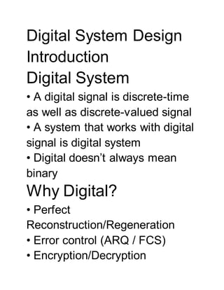
  • 1. Digital System Design Introduction Digital System • A digital signal is discrete-time as well as discrete-valued signal • A system that works with digital signal is digital system • Digital doesn’t always mean binary Why Digital? • Perfect Reconstruction/Regeneration • Error control (ARQ / FCS) • Encryption/Decryption
  • 2. Advantages of Digital System • Easy to store and retrieve digital information • Easy to process digital data • Digital is less error prone • Error can be controlled • Noise does not accumulate from one logic stage to next as it does in analog system (Regeneration) • The ease of large scale fabrication • Can be processed by a general purpose processor Analog vs. Digital
  • 3. design • Digital design need to handle with only few specified (mostly two) logic levels – It is less important to precisely simulate resistive, capacitive and inductive parameters – Design simulation can be based on the logic only, tools can therefore follow the truth tables Analog vs. Digital design • Analog design requires precise voltage and current
  • 4. characteristics of the devices – Parasitic capacitance, resistance, inductance are very important – Circuit elements are non-linear – Design verifications require complex simulations involving solutions of differential equations Integrated Circuits Integrated Circuit (IC) • A set of electronic circuits on one small plate ("chip") of semiconductor material, usually silicon • Much smaller than a discrete circuit
  • 5. made from independent electronic components • ICs can be made very compact, having up to several billion transistors and other electronic components in a very small area • The width of each conducting line in a circuit is being smaller and smaller as the technology advances (from micrometer to nanometer) • In 2008 it was dropped below 100 nanometers, and has now been
  • 6. reduced to tens of nanometers Why ICs • Let a recent PC is more than 1000 times faster than that in 1982 then: – If one small table was required to set a PC in 1982, now does it requires more than 1000 tables to set a PC? – If a PC in 1982 consumed one unit of power, now does it need to supply more than 1000 unit of power? Why ICs • 80286 microprocessor – released on February 1982 – with
  • 7. 134,000 number of transistors • Pentium Pro microprocessor – released on November 1995 – with 5,500,000 number of transistors Why ICs • Electronic systems are backbone of many systems today, and it is a continuous trend towards digital electronics solutions in all areas of our life – Car electronics
  • 8. which includes music system, engine and dashboard controls – Electronics in aircraft, Washing Machines, Computing and Computers etc. – Communication, Phones, entertainment, TVs, measurements (instrumentation) etc. Properties of IC • Size: – Integrated circuits are much smaller, both
  • 9. transistors and wires are shrink to micrometer (or even nanometer) sizes within IC – Smaller size leads to advantages in speed and power consumption, because smaller components have smaller parasitic capacitances, resistances Properties of IC • Speed: – Signals can be switched between logic 0 and logic1 much quicker within a chip – Communications within a chip can occur hundreds of times faster than communication between chips –
  • 10. The high speed within chip is possible due to their small size. The smaller components and wires have smaller parasitic capacitances to slow down the signal Properties of IC • Power consumption: – Logic operations within a chip takes much less power – Due to small size of circuits on the chip-smaller parasitic capacitances and resistances
  • 11. requires less power to drive them Advantages of ICs • Small physical size • High speed • Low power consumption • Reduced cost • High reliability • Good performance Properties of Digital Circuits Properties of Digital Circuits • The binary output signal must
  • 12. be a prescribed function of the binary input or inputs • Quantization of amplitudes within the normal range of operating voltage is required, which implies strong nonlinearities in circuit operation Properties of Digital Circuits • Amplitude levels are regenerated in passing from the input to the output of a digital circuit • Changes in an output level
  • 13. should not appear at any unchanging input of the same circuit; there must be an explicit, unilateral cause- effect relationship between input(s) and output(s) Properties of Digital Circuits • The output of one circuit must be capable of driving more than one input of similar circuits • The number that can be driven
  • 14. is termed as fan-out of the circuit • The digital circuits must be capable of accepting more than one input, the number of independent input nodes is termed as fan-in Modern Electronics Development Modern Electronics
  • 15. Development • The invention of transistor at Bell Telephone Laboratories in 1947 • The introduction of bipolar transistor by Schockley in 1949 • 1956 the first bipolar digital logic gate by Harris • The first truly successful IC logic family, TTL (transistor transistor logic) was pioneered in 1962 • Other logic families were devised for higher performance i.e. ECL (emitter coupled logic) – first
  • 16. subnanosecond digital gates Modern Electronics Development • TTL had the advantage of offering higher integration density and was the basis of first integrated circuit revolution • Ultimately, in bipolar digital logic, the large power consumption per gate puts an upper limit on the number of gates that can be
  • 17. reliably integrated on a single die or package • The attempts were made to develop high integration density, low-power bipolar families (such as I2L – Integrated Injection Logic) Modern Electronics Development • The torch was gradually passed to the MOS digital integrated circuit approach
  • 18. • The basic principle behind the MOSFET transistor was proposed in a patent by J. Lilienfeld (Canada) as early as 1925, and independently by O. Heil in England in 1935 • Insufficient knowledge of materials and gate stability problems delayed the practical usability of the device for long
  • 19. time Modern Electronics Development • The next age of the digital integrated circuit revolution was inaugurated with the introduction of the first microprocessors by Intel in 1972 the 4004 and in 1974 the 8080 • MOS technology enabled the realization of the first high-density semiconductor memories • The large majority of the current integrated circuits are implemented in the MOS technology Moore’s Law
  • 20. • Gordon Moore: co-founder of Intel • In 1960, he predicted that number of transistors per chip would grow exponentially (double every 18 months) • This prediction later called Moore’s law, has proven to be amazingly visionary • Integration complexity doubles approximately every 1 to 2 years, as a result, memory density has increased by more than a
  • 21. thousand-fold since 1970 Evolution in Complexity Evolution in Transistor Count Evolution in Speed/Performance 10 μm – 1971 6 μm – 1974 3 μm – 1977 1.5 μm – 1982 1 μm – 1985 800 nm – 1989 600 nm –
  • 22. 1994 350 nm – 1995 250 nm – 1997 180 nm – 1999 130 nm – 2001 90 nm – 2004 65 nm – 2006 45 nm – 2008 32 nm – 2010 22 nm – 2012 14 nm – 2014 10 nm – 2016–2017 7 nm – 2017–2018 5 nm – 2020–2021 Hierarchical Design • Divide and conquer approach
  • 23. • Design complexity is reduced by breaking it down into manageable pieces • Example: – A 32 bit ripple carry counter design is specified as 32 flip flops – Each flip flop is specified as connection of several gates – Each gate as connection of transistors Design Abstraction • Multiple levels of design abstraction are given for the ICs
  • 24. • Design abstraction goes from the specifications to layout (or the physical design) Design Abstraction for the ICs Specifications Behavior RTL specs Logic Circuit Layout Natural language Complexity HDL Finite State Machine List of gates Abstraction
  • 25. Transistor level circuit With EDA tools, design abstraction can be high Physical realization and lower level can be synthesized Design Abstraction Levels MODULE + GATE CIRCUIT DEVICE G S n+ n+ SYSTEM D Design Techniques • Two contradicting issues – increasing complexity of the designs – reducing time for design
  • 26. • Only possible solutions are – increase more and more automation – multiple levels of abstraction for design to eliminate unnecessary details Electronic Design Automation (EDA) Electronic Design Automation (EDA) • Automation of the Electronic Design • A category of software tools for designing electronic systems
  • 27. i.e. printed circuit boards and integrated circuits • The tools work together in a design flow that chip designers use to design and analyze entire semiconductor chips • Also referred to as "Electronic Computer- Aided Design" (ECAD) EDA
  • 28. • Transistor simulation: low-level transistor- simulation of a schematic/layout's behavior at device-level • Logic simulation: digital- simulation of an RTL or gate's digital (Boolean 0/1) behavior, at Boolean-level • Behavioral Simulation: high- level simulation of a design's architectural operation EDA • Issues – Devices: transistors, gates, flip flops, digital building blocks, memory,
  • 29. processors etc. – Levels: Chip, Board, System, Concept – Simplicity: Custom Design vs. reuse of design • EDA focus is mainly on digital circuit design though analog is getting in EDA • With high speed designs, various other issues are also important – Interconnect resistance and capacitance – RF interference, induced currents etc. • EDA need to take care of this
  • 30. using various simulation • Before EDA, integrated circuits were designed by hand, and manually laid out – time consuming and difficult EDA Examples • EAGLE for PCB Design by CadSoft Computer • National Instruments Electronics Workbench Group – NI Multisim - schematic capture and simulation – NI Ultiboard -
  • 31. printed circuit board layout editor • Advanced Design System for high frequency and high speed design by Keysight Technologies Digital System and Characteristics Requirements • Highly reliable • Low power consumption • Small size • High speed • Low cost and • High performance But there is trade-offs between requirements
  • 32. Choices • Logic family – What are the permissible tradeoffs ? • Level of integration – How many functions? • Programmable versus fixed function circuits – What is the context? Logic families • Various logic families are: – Diode Logic – Diode Transistor Logic (DTL) – Resistor Transistor Logic (RTL) – Transistor Transistor Logic (TTL) – Emitter coupled logic (ECL) – Integrated Injection Logic
  • 33. (I2L) – MOS:- NMOS, PMOS and CMOS Level of integration • Small-scale integration (SSI): no of gates less than 10 – Simple logic functions, basic storage elements etc. • Medium-scale integration (MSI): 10–100 gates – 4-bit adders, 8-to-1 multiplexers, counters, etc. • Large-scale integration (LSI): 100 to a few 1000 gates – Programmable logic array (PLA), PROM, small processors, etc. • Very large-scale integration (VLSI):
  • 34. several thousand to millions of gates – Processors, large memory array, etc. • Ultra large-scale integration (ULSI): no of gates > 10 million – Advanced processors, system chips, etc. An ideal logic element • Operates from a single power source • Draws a minimum of power, ideally zero • The two binary output levels are 0 and vDD Vcc
  • 35. inputs output Gnd Out VDD VDD/2 In contd... • The output impedance is low, so that large current may be delivered to external loads without altering the output voltage levels • The transition between states at output occurs abruptly for an input level equal to one half the supply voltage contd...
  • 36. • There is no time delay between the input transition and the consequent output transition • Virtually any numbers of inputs are available; the input impedance is high so that the circuit imposes little loading on the driving signal Noise and noise margin • Noise:- – Any unwanted signal added to vary voltage or currents at logic nodes – If the magnitude of noise is high it will cause logic
  • 37. errors contd... • Noise margin:- – The maximum noise voltage level that a logic signal can tolerate without any error – If the noise amplitude at input at any logic is smaller than noise margin (a specified critical magnitude) the noise amplitude will be attenuated – High- level noise margin: NMH=VOH - VIH – Low-level noise margin: NML=VIL - VOL
  • 38. Vcc(5 V) Vec(5 V) H VOH (2.4) High noise margin VIH (2.0) VIL (0.8) VOL (0.4) Low noise margin GND (0) GND (0) Output voltage range Input voltage range Mutual inductance with another logic node
  • 39. --Inductive and resistive drops -Capacitive coupling from another node 3 Radio frequency signals from external sources Transient characteristics • Rise time – Time taken by the signal to switch from 10% to 90% of its normal value • Fall time – Time taken by the signal to switch from 90% to 10% of its normal value • High-low and low-high
  • 40. transition times at the output of a gate are defined as tHL and tLH Transient characteristics • Propagation delay – It takes certain amount of time to propagate from input to the output – Propagation delay is the average transition delay for a signal to propagate from input to output when the binary signals change in value – tPHL, tPLH and tPD • tPHL:- the time required for the
  • 41. output signal to reach 50% of its normal value on the H-to-L transition after the input signal reached 50% of its normal signal • tPLH:- the time required for the output signal to reach 50% of its normal value on the L-to-H transition after the input signal reached 50% of its
  • 42. normal signal • tPD:- It is the mean of the above two and is generally used for hand calculations. And in early days max of the two quantities was considered Propagation delay for an Inverter High-to-low (tPHL) and low-to-high (tPLH) propagation delays are measured on output transitions Power
  • 43. • Power supply (VCC) – Power required by the circuit to operate • Power dissipation – Power consumed by the circuit – Each gate can be at any of these three states, high, transition and low states – And the current flowing at high stage may be Icch, that at transition is Icct and at low is Iccl • In MOS – The transient current is maximum – Pavg=Vcc*Icct • In TTL and older families – Icct<<Icch and Icct <<Iccl –
  • 44. Pavg=Vcc*(Icch + Iccl)/2 Power delay product • Power delay product PDP is the product of power consumption (avg) and average propagation delay o PDP=Pd(avg)*tpd Fan-in and Fan-out • Fan-in:- number of inputs available to a gate • Fan-out:- number of outputs the gate can drive Logic Families Logic families
  • 45. • Various logic families are: – Diode Logic – Resistor Transistor Logic (RTL) – Diode Transistor Logic (DTL) – Transistor Transistor Logic (TTL) – Emitter coupled logic (ECL) – Integrated Injection logic (IIL) – MOS:- NMOS, PMOS and CMOS contd.... • For the comparison of various logic families the following parameters should be considered – Speed (propagation delay time) – Noise immunity – Fan in and fan out – Power supply requirements – Power dissipation per gate
  • 46. contd.... – Number of functions available – Maximum frequency at which sequential circuits operate – Components packing density – Cost Diode logic • In the early days (by 1950) diode logic were used • Diodes were cheaper than transistors • However the diode logic were followed by transistors to eliminate some disadvantages • With the advent of SSI in 1960,
  • 47. the cost of diodes and transistors were equalized Diode OR logic Diode AND logic Simple Diode Logic • Advantages – Diodes were cheap ⇒ cheap Diode Logic – Diode logic is simple • Disadvantages – They degrade digital signals (there is no signal reconstruction) – The output terribly follows the inputs – NOT gate can not be performed • So diode logic were replaced by advanced logic Resistor transistor logic • The first form of digital ICs to
  • 48. receive general usage • Was invented in 1962 • Each input was associated with one resistor and the output stage had transistors • If the input is low then the transistor will be cut-off and the output will be high • If the input is high enough to drive the transistor to saturation then the output is low RTL NOT gate RTL NAND RTL NOR • They are simple and remain inexpensive • They do draw a significant
  • 49. amount of current from the power supply for each gate • The fan-out of RTL gate is limited by the value of the output voltage when high RTL characteristics (typical) • Supply voltage = 3.6 V • Fan out = 5 • Propagation delay tPD = 25 ns • Power dissipation/gate = 12
  • 50. mW • VOH/VOL= 1.2V/0.2V • VIH/VIL = 0.8/0.7V • NMH/NML = 0.4/0.5V Diode transistor logic • Each input is associated with one diode • Input stage has diode(s) and the output has transistor(s) • NAND and NOR functions, which are easy to build in DTL, are logically complete • Any logical function can be expressed
  • 51. • This logic family uses lower voltages, less power