
Recommended
Recommended
More Related Content
What's hot
What's hot (12)
Similar to Enhancing magnetic and electric properties of Type-II superconductors
Similar to Enhancing magnetic and electric properties of Type-II superconductors (20)
More from NanoFrontMag-cm
More from NanoFrontMag-cm (18)
Recently uploaded
Recently uploaded (20)
Enhancing magnetic and electric properties of Type-II superconductors
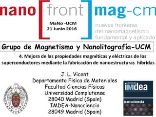
- 1. J. L. Vicent Departamento Fisica de Materiales Facultad Ciencias Físicas Universidad Complutense 28040 Madrid (Spain) IMDEA-Nanociencia 28049 Madrid (Spain) Grupo de Magnetismo y Nanolitografía-UCM 4. Mejora de las propiedades magnéticas y eléctricas de los superconductores mediante la fabricación de nanoestructuras híbridas
- 2. Type II Supercondutors Vortices Mixed State Tc Mixed State Normal State Meissner State Hc2 Hc1 NbSe2 Hess et al. PRL62,214 (1989) Abrikosov Lattice Hc1<H<Hc2 Mixed State Vortices on the move ?
- 3. vBE Magnetic Field VDC R(H) B B 0 Current Density J oL JF v J E FL ,v Vortices move J Bc1<B<Bc2 Mixed State Vortex motion causes energy dissipation: Resistance ≠ 0 &
- 4. Magnetic pinning Local depression of the superconductivity Core pinning r2 Js ns(r) H 0=h/2e=2.067×10-15 Wb Superconducting energy is minimized by locating vortices in defects PINNING MECHANISMSVortex structure sketch
- 5. Pinning center Minimum of potential Pinning Force Fp Decrease vortex velocity Minimum in Resistance 0 FL Fp V(x) R -4 -3 -2 -1 1 2 3 4 5-5 -0.6 -0.4 -0.2 0.0 0.2 0.4 0.6 10 -5 10 -4 10 -3 10 -2 10 -1 10 0 R() H(kOe) Superconductor Defect Película de Nb Array dots Si 100 nm
- 6. -0.6 -0.4 -0.2 0.0 0.2 0.4 0.6 10 -5 10 -4 10 -3 10 -2 10 -1 10 0 R() H(kOe) Rectangular lattice a=400nm b=600nm ΔH = 85.3 Oe a b S 0 0 0 0 axb n Hn 0 Minima in Resistance Vortex density =n· Pinning center density -4 -3 -2 -1 1 2 3 4 5-5 0n S n B Matching Fields Vortex lattice u.c. areaS n = Vortices per u.c. 0.99Tc 100 mA 100 nm Nb + 40 nm Ni dots
- 7. Superconductor Nb Defectos: Cu, Si, Ni, Co, Py, a-NdCo5, Co/Pd (multicapas)
- 8. Magnetism enhances superconductivity Field induced superconductivity V AV Lange, van Bael, Bruynseraede,Moshchalkov PRL 90 (2003) H=0 H0 SC SC Superconductor Superconductor Magnets with out of plane Mz Magnets with out of plane Mz
- 9. Dot Co/Pd Nb -0.4 -0.2 0.0 0.2 0.4 10 -3 10 -2 10 -1 10 0 10 mA 20 mA 50 mA 100 mA R() H (kOe) -2 -1 0 1 2 10 -4 10 -3 10 -2 10 -1 10 0 Desimanado Imanado R/RN H/Hmatching Dot Si Nb
- 10. -0,4 -0,3 -0,2 -0,1 0,0 0,1 0,2 0,3 0,4 10 -5 10 -4 10 -3 10 -2 10 -1 10 0 +Msat -Msat R() H(kOe) Pinning en N= -1 para distintas memorias magneticas de los dots 2.5 mA T=0.99Tc Tc=8.385 K Array of Ni dots (400 nm x 400 nm) /Nb film +1 -1 Dot Ni Nb Nb Nb
- 11. -0.15 -0.10 -0.05 0.00 0.05 0.10 0.15 0.0 1.0x10 -3 2.0x10 -3 3.0x10 -3 Desde -3 kOe Desde -1 kOe Desde -0.4 kOe Desde -0.3 kOe Desde -0.25 kOe Desde 2 kOe Desde 0.8 kOe Desde 0.5 kOe Desde 0.35 kOe Desde 0.25 kOe R() H(kOe) Pinning en N= -1 para distintas memorias magneticas de los dots 2.5 mA T=0.99Tc Tc=8.385 K Dot Ni Nb Nb Nb -0,4 -0,3 -0,2 -0,1 0,0 0,1 0,2 0,3 0,4 10 -5 10 -4 10 -3 10 -2 10 -1 10 0 +Msat -Msat R() H(kOe) Pinning en N= -1 para distintas memorias magneticas de los dots 2.5 mA T=0.99Tc Tc=8.385 K
- 12. Three-state memory nanodevice: +1 (M =+Mz); 0 (M = 0); -1 (M =-Mz); Reading nanodevice: Zero output signal (VDC = 0) for specific value of Happl which depends on how the device is built. Happl.= 0 Happl.≠ 0 Input signals: ac currents Output signals: dc voltages Nb/(Co/Pd)
- 13. -1,0 -0,5 0,0 0,5 1,0 -20 -10 0 10 20 Vdc,max(mV) MR / MS 1 2 3 4 5 6 -20 -10 0 10 20 V dc (mV) I ac (mA) MR/MS = 0.65 - Vdc, max +Vdc, max del Valle et al. Sci. Rep. (2015) +1 0 -1 T = 0.99Tc Remanent magnetic states control ratchet effects
- 14. 8.40 8.42 8.44 8.46 8.48 8.50 8.52 0 100 200 300 400 500 T(K) H(Oe) R / RN 0.0 0.5 1.0 Hcompensation = 240 Oe Hmatching= 36 Oe A C B C B A Hcompensation and Hmatching depend on the sample design. Happl
- 15. R / RN 0.0 0.5 1.0 8,42 8,44 8,46 8,48 8,50 8,52 0 100 200 300 400 500 T(K) H(Oe) 0 100 200 300 400 -20 -10 0 10 20 Vdc,max(mV) H (Oe) -1,0 -0,5 0,0 0,5 1,0 -20 -10 0 10 20 Vdc,max(mV) MR / MS +1 0 -1 Happl = 0 Closing….
- 16. AAlicia Gomez Javier del V Javier del Valle JaviEer del VElvira Gonzalez
- 17. The END