SlideShare a Scribd company logo
1 of 7
Download to read offline
EECS 522
CAD#3
Nagarjun Bhat
UMID: 76047405
Design:
First, the symmetric inductor was analyzed in Cadence separately to find its peak quality factor and from that the
parasitic series resistance Rs was calculated. From the formula in handout, the equivalent parallel resistance was
obtained and gm of the transistors decided on this basis to obtain oscillation.
At the same time, setting an Ibias of 3mA, and using the given spec of Vpp needed, Rp was obtained. And once again the
gm of the transistors extracted. The best of these values which gave the desired Phase noise performance was chosen
for final design.
The design was later optimized for lower power consumption, w9ith changes in biasing voltages.
Shown below is the schematic of the design:
Figure 1: Schematic of the designed VCO
Passives used: Symmetric Inductor, Dualmimcap-1 nos and Ncap (as varactor)-2Nos.
The PSS and Pnoise analyses were run on the schematic and then layout and a good conformation was obtained.
EECS 522
CAD#3
Nagarjun Bhat
UMID: 76047405
The Table below summarizes the values of devices used in the design
Name/Device Dimensions Value
T3/ NFET_RF W=30u, L=130n, Nf=10 Region:2 Id=3.68mA
T5/ NFET_RF W=30u, L=130n, Nf=10 Region:2 Id=3.68mA
T4/ NFET_RF W=30u, L=130n, Nf=10 Region:2 Id=3.68mA
Symindp/Symmetric Stacked Inductor with Centre Tap W=285u,L=8.5u, N=5 L=6.78nH
CM13/DualmimCap W=32.03u, L=18u Cap=3.3pF
CN0 W=16u, L=9u Cap=1.5pF
CN2 W=16u, L=9u Cap=1.5pF
Table 1: Specifications of all devices used
Shown below are the results obtqained from simulation of the schematic.
Figure 2: Schematic tuning range
EECS 522
CAD#3
Nagarjun Bhat
UMID: 76047405
Figure 3: Oscillation amp@915MHz_ schematic (Vpp=5Vpp) and Phase noise from schematic
Figure 4: Phase_Noise_902MHz and 928MHz(right)
EECS 522
CAD#3
Nagarjun Bhat
UMID: 76047405
Layout
Figure 5: Layout of VCO, zoomed on the right
The layout is both DRC and LVS clean!
Figure 6: DRC Clean
EECS 522
CAD#3
Nagarjun Bhat
UMID: 76047405
Figure 7: LVS Clean
POST PEX RESULTS:
The following table summarizes all the specifications and performance of the designed VCO
Power Consumed Post PEX: 4.3mW
Area: 0406mm X 0.335mm=0.1362mm2
Vbias1=800m
Vbias2=NA
Vtune:0-1.2V
Specification Pre-PEX Post-PEX
Tuning Range 900MHz-928MHz 890MHz-930MHz
Phase Noise -160dBc @1MHz offset for f0=902MHz
-156dBc @1MHz offset for f0=915MHz
-149dBc @1MHz offset for f0=928MHz
-158dBc @1MHz offset for f0=902MHz
-159dBc @1MHz offset for f0=915MHz
-150dBc @1MHz offset for f0=928MHz
Differential Op 3.4Vpp 2.82Vpp,3Vpp,3.1Vpp
EECS 522
CAD#3
Nagarjun Bhat
UMID: 76047405
Figure 8: Post PEX_Tuning range and Phase noise for all frequencies Post PEX
Figure 9: Post PEX Phase Noise,@f0=902MHz and 2.818Vpp for 902MHz_Post PEX
EECS 522
CAD#3
Nagarjun Bhat
UMID: 76047405
Figure 10: Phase Noise_915MHz_schematic and Vpp=3.16V for @f0=915MHz, Post PEX
Figure 11: Phase noise @f0=928MHz, post PEX and Vpp=3.1V @ 928MHz, post PEX

More Related Content

What's hot

Design of a Fully Differential Folded-Cascode Operational Amplifier
Design of a Fully Differential Folded-Cascode Operational AmplifierDesign of a Fully Differential Folded-Cascode Operational Amplifier
Design of a Fully Differential Folded-Cascode Operational AmplifierSteven Ernst, PE
 
Project1
Project1Project1
Project1Rx H
 
Ece593 project1 chien_chun_yao_and_karthikvel_rathinavel
Ece593 project1 chien_chun_yao_and_karthikvel_rathinavelEce593 project1 chien_chun_yao_and_karthikvel_rathinavel
Ece593 project1 chien_chun_yao_and_karthikvel_rathinavelKarthik Rathinavel
 
Neutral point clamped inverter
Neutral point clamped inverterNeutral point clamped inverter
Neutral point clamped inverterZunAib Ali
 
Single Stage Differential Folded Cascode Amplifier
Single Stage Differential Folded Cascode AmplifierSingle Stage Differential Folded Cascode Amplifier
Single Stage Differential Folded Cascode AmplifierAalay Kapadia
 
Design of 17-Bit Audio Band Delta-Sigma Analog to Digital Converter
Design of 17-Bit Audio Band Delta-Sigma Analog to Digital ConverterDesign of 17-Bit Audio Band Delta-Sigma Analog to Digital Converter
Design of 17-Bit Audio Band Delta-Sigma Analog to Digital ConverterKarthik Rathinavel
 
Two stage folded cascode op amp design in Cadence
Two stage folded cascode op amp design in CadenceTwo stage folded cascode op amp design in Cadence
Two stage folded cascode op amp design in CadenceKarthik Rathinavel
 
Design and implementation of cmos rail to-rail operational amplifiers
Design and implementation of cmos rail to-rail operational amplifiersDesign and implementation of cmos rail to-rail operational amplifiers
Design and implementation of cmos rail to-rail operational amplifiersGrace Abraham
 
Power converter report
Power converter reportPower converter report
Power converter reportZunAib Ali
 
Design of a Sample and Hold Circuit using Rail to Rail Low Voltage Compact Op...
Design of a Sample and Hold Circuit using Rail to Rail Low Voltage Compact Op...Design of a Sample and Hold Circuit using Rail to Rail Low Voltage Compact Op...
Design of a Sample and Hold Circuit using Rail to Rail Low Voltage Compact Op...IJERA Editor
 
DESIGNED A 350NM TWO STAGE OPERATIONAL AMPLIFIER
DESIGNED A 350NM TWO STAGE OPERATIONAL AMPLIFIERDESIGNED A 350NM TWO STAGE OPERATIONAL AMPLIFIER
DESIGNED A 350NM TWO STAGE OPERATIONAL AMPLIFIERIlango Jeyasubramanian
 
Three phase bridge controlled by microprocessor(eee499.blogspot.com)
Three phase bridge controlled by microprocessor(eee499.blogspot.com)Three phase bridge controlled by microprocessor(eee499.blogspot.com)
Three phase bridge controlled by microprocessor(eee499.blogspot.com)slmnsvn
 
IRJET-Two stage Cascade BJT Amplifier
IRJET-Two stage Cascade BJT AmplifierIRJET-Two stage Cascade BJT Amplifier
IRJET-Two stage Cascade BJT AmplifierIRJET Journal
 
SIMULATIONS AND PRACTICAL DESIGNS OF OFF.LINE CONVERTERS-THE FRONT END
SIMULATIONS AND PRACTICAL DESIGNS OF OFF.LINE CONVERTERS-THE FRONT ENDSIMULATIONS AND PRACTICAL DESIGNS OF OFF.LINE CONVERTERS-THE FRONT END
SIMULATIONS AND PRACTICAL DESIGNS OF OFF.LINE CONVERTERS-THE FRONT ENDTsuyoshi Horigome
 

What's hot (20)

Design of a Fully Differential Folded-Cascode Operational Amplifier
Design of a Fully Differential Folded-Cascode Operational AmplifierDesign of a Fully Differential Folded-Cascode Operational Amplifier
Design of a Fully Differential Folded-Cascode Operational Amplifier
 
Project1
Project1Project1
Project1
 
Chapter 7
Chapter 7Chapter 7
Chapter 7
 
FINALREPORTOPAMP.docx(1)
FINALREPORTOPAMP.docx(1)FINALREPORTOPAMP.docx(1)
FINALREPORTOPAMP.docx(1)
 
Folded cascode1
Folded cascode1Folded cascode1
Folded cascode1
 
Ece593 project1 chien_chun_yao_and_karthikvel_rathinavel
Ece593 project1 chien_chun_yao_and_karthikvel_rathinavelEce593 project1 chien_chun_yao_and_karthikvel_rathinavel
Ece593 project1 chien_chun_yao_and_karthikvel_rathinavel
 
Neutral point clamped inverter
Neutral point clamped inverterNeutral point clamped inverter
Neutral point clamped inverter
 
Emec 1 (2)
Emec 1 (2)Emec 1 (2)
Emec 1 (2)
 
Single Stage Differential Folded Cascode Amplifier
Single Stage Differential Folded Cascode AmplifierSingle Stage Differential Folded Cascode Amplifier
Single Stage Differential Folded Cascode Amplifier
 
Design of 17-Bit Audio Band Delta-Sigma Analog to Digital Converter
Design of 17-Bit Audio Band Delta-Sigma Analog to Digital ConverterDesign of 17-Bit Audio Band Delta-Sigma Analog to Digital Converter
Design of 17-Bit Audio Band Delta-Sigma Analog to Digital Converter
 
Two stage folded cascode op amp design in Cadence
Two stage folded cascode op amp design in CadenceTwo stage folded cascode op amp design in Cadence
Two stage folded cascode op amp design in Cadence
 
Design and implementation of cmos rail to-rail operational amplifiers
Design and implementation of cmos rail to-rail operational amplifiersDesign and implementation of cmos rail to-rail operational amplifiers
Design and implementation of cmos rail to-rail operational amplifiers
 
Power converter report
Power converter reportPower converter report
Power converter report
 
Design of a Sample and Hold Circuit using Rail to Rail Low Voltage Compact Op...
Design of a Sample and Hold Circuit using Rail to Rail Low Voltage Compact Op...Design of a Sample and Hold Circuit using Rail to Rail Low Voltage Compact Op...
Design of a Sample and Hold Circuit using Rail to Rail Low Voltage Compact Op...
 
Space vector PWM
Space vector PWMSpace vector PWM
Space vector PWM
 
DESIGNED A 350NM TWO STAGE OPERATIONAL AMPLIFIER
DESIGNED A 350NM TWO STAGE OPERATIONAL AMPLIFIERDESIGNED A 350NM TWO STAGE OPERATIONAL AMPLIFIER
DESIGNED A 350NM TWO STAGE OPERATIONAL AMPLIFIER
 
Dv4301732734
Dv4301732734Dv4301732734
Dv4301732734
 
Three phase bridge controlled by microprocessor(eee499.blogspot.com)
Three phase bridge controlled by microprocessor(eee499.blogspot.com)Three phase bridge controlled by microprocessor(eee499.blogspot.com)
Three phase bridge controlled by microprocessor(eee499.blogspot.com)
 
IRJET-Two stage Cascade BJT Amplifier
IRJET-Two stage Cascade BJT AmplifierIRJET-Two stage Cascade BJT Amplifier
IRJET-Two stage Cascade BJT Amplifier
 
SIMULATIONS AND PRACTICAL DESIGNS OF OFF.LINE CONVERTERS-THE FRONT END
SIMULATIONS AND PRACTICAL DESIGNS OF OFF.LINE CONVERTERS-THE FRONT ENDSIMULATIONS AND PRACTICAL DESIGNS OF OFF.LINE CONVERTERS-THE FRONT END
SIMULATIONS AND PRACTICAL DESIGNS OF OFF.LINE CONVERTERS-THE FRONT END
 

Similar to Low_Noise_VCO

Design and analysis of low power pseudo differential
Design and analysis of low power pseudo differentialDesign and analysis of low power pseudo differential
Design and analysis of low power pseudo differentialeSAT Publishing House
 
Simulation of 3 bit Flash ADC in 0.18μmTechnology using NG SPICE Tool for Hig...
Simulation of 3 bit Flash ADC in 0.18μmTechnology using NG SPICE Tool for Hig...Simulation of 3 bit Flash ADC in 0.18μmTechnology using NG SPICE Tool for Hig...
Simulation of 3 bit Flash ADC in 0.18μmTechnology using NG SPICE Tool for Hig...ijsrd.com
 
LowNoiseAmplifierReport
LowNoiseAmplifierReportLowNoiseAmplifierReport
LowNoiseAmplifierReportSyed Kazmi
 
Design and Implementation of Single Phase AC-DC Buck-Boost Converter for Powe...
Design and Implementation of Single Phase AC-DC Buck-Boost Converter for Powe...Design and Implementation of Single Phase AC-DC Buck-Boost Converter for Powe...
Design and Implementation of Single Phase AC-DC Buck-Boost Converter for Powe...IJPEDS-IAES
 
Modeling and simulation of three phases cascaded H-bridge grid-tied PV inverter
Modeling and simulation of three phases cascaded H-bridge grid-tied PV inverterModeling and simulation of three phases cascaded H-bridge grid-tied PV inverter
Modeling and simulation of three phases cascaded H-bridge grid-tied PV inverterjournalBEEI
 
Design of 6 bit flash analog to digital converter using variable switching vo...
Design of 6 bit flash analog to digital converter using variable switching vo...Design of 6 bit flash analog to digital converter using variable switching vo...
Design of 6 bit flash analog to digital converter using variable switching vo...VLSICS Design
 
Total Harmonic Distortion Analysis of Multilevel Inverter Fed To Induction Mo...
Total Harmonic Distortion Analysis of Multilevel Inverter Fed To Induction Mo...Total Harmonic Distortion Analysis of Multilevel Inverter Fed To Induction Mo...
Total Harmonic Distortion Analysis of Multilevel Inverter Fed To Induction Mo...IJERA Editor
 
VHDL Implementation of Capacitor Voltage Balancing Control with Level-Shifted...
VHDL Implementation of Capacitor Voltage Balancing Control with Level-Shifted...VHDL Implementation of Capacitor Voltage Balancing Control with Level-Shifted...
VHDL Implementation of Capacitor Voltage Balancing Control with Level-Shifted...IAES-IJPEDS
 
Modeling and simulation of three phases cascaded H-bridge grid-tied PV inverter
Modeling and simulation of three phases cascaded H-bridge grid-tied PV inverterModeling and simulation of three phases cascaded H-bridge grid-tied PV inverter
Modeling and simulation of three phases cascaded H-bridge grid-tied PV inverterjournalBEEI
 
Comparative Study of CMOS Op-Amp In 45nm And 180 Nm Technology
Comparative Study of CMOS Op-Amp In 45nm And 180 Nm TechnologyComparative Study of CMOS Op-Amp In 45nm And 180 Nm Technology
Comparative Study of CMOS Op-Amp In 45nm And 180 Nm TechnologyIJERA Editor
 
Assignment 1 Description Marks out of Wtg() Due date .docx
Assignment 1  Description Marks out of Wtg() Due date .docxAssignment 1  Description Marks out of Wtg() Due date .docx
Assignment 1 Description Marks out of Wtg() Due date .docxfredharris32
 
Power System Simulation Laboratory Manual
Power System Simulation Laboratory Manual Power System Simulation Laboratory Manual
Power System Simulation Laboratory Manual Santhosh Kumar
 

Similar to Low_Noise_VCO (20)

506 267-276
506 267-276506 267-276
506 267-276
 
Design and analysis of low power pseudo differential
Design and analysis of low power pseudo differentialDesign and analysis of low power pseudo differential
Design and analysis of low power pseudo differential
 
Project report. fin
Project report. finProject report. fin
Project report. fin
 
Simulation of 3 bit Flash ADC in 0.18μmTechnology using NG SPICE Tool for Hig...
Simulation of 3 bit Flash ADC in 0.18μmTechnology using NG SPICE Tool for Hig...Simulation of 3 bit Flash ADC in 0.18μmTechnology using NG SPICE Tool for Hig...
Simulation of 3 bit Flash ADC in 0.18μmTechnology using NG SPICE Tool for Hig...
 
100 w sspa
100 w sspa100 w sspa
100 w sspa
 
LowNoiseAmplifierReport
LowNoiseAmplifierReportLowNoiseAmplifierReport
LowNoiseAmplifierReport
 
Design and Implementation of Single Phase AC-DC Buck-Boost Converter for Powe...
Design and Implementation of Single Phase AC-DC Buck-Boost Converter for Powe...Design and Implementation of Single Phase AC-DC Buck-Boost Converter for Powe...
Design and Implementation of Single Phase AC-DC Buck-Boost Converter for Powe...
 
Modeling and simulation of three phases cascaded H-bridge grid-tied PV inverter
Modeling and simulation of three phases cascaded H-bridge grid-tied PV inverterModeling and simulation of three phases cascaded H-bridge grid-tied PV inverter
Modeling and simulation of three phases cascaded H-bridge grid-tied PV inverter
 
Design of 6 bit flash analog to digital converter using variable switching vo...
Design of 6 bit flash analog to digital converter using variable switching vo...Design of 6 bit flash analog to digital converter using variable switching vo...
Design of 6 bit flash analog to digital converter using variable switching vo...
 
07
0707
07
 
Kf3617641768
Kf3617641768Kf3617641768
Kf3617641768
 
finalreport
finalreportfinalreport
finalreport
 
Total Harmonic Distortion Analysis of Multilevel Inverter Fed To Induction Mo...
Total Harmonic Distortion Analysis of Multilevel Inverter Fed To Induction Mo...Total Harmonic Distortion Analysis of Multilevel Inverter Fed To Induction Mo...
Total Harmonic Distortion Analysis of Multilevel Inverter Fed To Induction Mo...
 
VHDL Implementation of Capacitor Voltage Balancing Control with Level-Shifted...
VHDL Implementation of Capacitor Voltage Balancing Control with Level-Shifted...VHDL Implementation of Capacitor Voltage Balancing Control with Level-Shifted...
VHDL Implementation of Capacitor Voltage Balancing Control with Level-Shifted...
 
Modeling and simulation of three phases cascaded H-bridge grid-tied PV inverter
Modeling and simulation of three phases cascaded H-bridge grid-tied PV inverterModeling and simulation of three phases cascaded H-bridge grid-tied PV inverter
Modeling and simulation of three phases cascaded H-bridge grid-tied PV inverter
 
Comparative Study of CMOS Op-Amp In 45nm And 180 Nm Technology
Comparative Study of CMOS Op-Amp In 45nm And 180 Nm TechnologyComparative Study of CMOS Op-Amp In 45nm And 180 Nm Technology
Comparative Study of CMOS Op-Amp In 45nm And 180 Nm Technology
 
525 192-198
525 192-198525 192-198
525 192-198
 
E04724148
E04724148E04724148
E04724148
 
Assignment 1 Description Marks out of Wtg() Due date .docx
Assignment 1  Description Marks out of Wtg() Due date .docxAssignment 1  Description Marks out of Wtg() Due date .docx
Assignment 1 Description Marks out of Wtg() Due date .docx
 
Power System Simulation Laboratory Manual
Power System Simulation Laboratory Manual Power System Simulation Laboratory Manual
Power System Simulation Laboratory Manual
 

Low_Noise_VCO

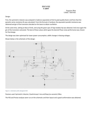
  • 1. EECS 522 CAD#3 Nagarjun Bhat UMID: 76047405 Design: First, the symmetric inductor was analyzed in Cadence separately to find its peak quality factor and from that the parasitic series resistance Rs was calculated. From the formula in handout, the equivalent parallel resistance was obtained and gm of the transistors decided on this basis to obtain oscillation. At the same time, setting an Ibias of 3mA, and using the given spec of Vpp needed, Rp was obtained. And once again the gm of the transistors extracted. The best of these values which gave the desired Phase noise performance was chosen for final design. The design was later optimized for lower power consumption, w9ith changes in biasing voltages. Shown below is the schematic of the design: Figure 1: Schematic of the designed VCO Passives used: Symmetric Inductor, Dualmimcap-1 nos and Ncap (as varactor)-2Nos. The PSS and Pnoise analyses were run on the schematic and then layout and a good conformation was obtained.
  • 2. EECS 522 CAD#3 Nagarjun Bhat UMID: 76047405 The Table below summarizes the values of devices used in the design Name/Device Dimensions Value T3/ NFET_RF W=30u, L=130n, Nf=10 Region:2 Id=3.68mA T5/ NFET_RF W=30u, L=130n, Nf=10 Region:2 Id=3.68mA T4/ NFET_RF W=30u, L=130n, Nf=10 Region:2 Id=3.68mA Symindp/Symmetric Stacked Inductor with Centre Tap W=285u,L=8.5u, N=5 L=6.78nH CM13/DualmimCap W=32.03u, L=18u Cap=3.3pF CN0 W=16u, L=9u Cap=1.5pF CN2 W=16u, L=9u Cap=1.5pF Table 1: Specifications of all devices used Shown below are the results obtqained from simulation of the schematic. Figure 2: Schematic tuning range
  • 3. EECS 522 CAD#3 Nagarjun Bhat UMID: 76047405 Figure 3: Oscillation amp@915MHz_ schematic (Vpp=5Vpp) and Phase noise from schematic Figure 4: Phase_Noise_902MHz and 928MHz(right)
  • 4. EECS 522 CAD#3 Nagarjun Bhat UMID: 76047405 Layout Figure 5: Layout of VCO, zoomed on the right The layout is both DRC and LVS clean! Figure 6: DRC Clean
  • 5. EECS 522 CAD#3 Nagarjun Bhat UMID: 76047405 Figure 7: LVS Clean POST PEX RESULTS: The following table summarizes all the specifications and performance of the designed VCO Power Consumed Post PEX: 4.3mW Area: 0406mm X 0.335mm=0.1362mm2 Vbias1=800m Vbias2=NA Vtune:0-1.2V Specification Pre-PEX Post-PEX Tuning Range 900MHz-928MHz 890MHz-930MHz Phase Noise -160dBc @1MHz offset for f0=902MHz -156dBc @1MHz offset for f0=915MHz -149dBc @1MHz offset for f0=928MHz -158dBc @1MHz offset for f0=902MHz -159dBc @1MHz offset for f0=915MHz -150dBc @1MHz offset for f0=928MHz Differential Op 3.4Vpp 2.82Vpp,3Vpp,3.1Vpp
  • 6. EECS 522 CAD#3 Nagarjun Bhat UMID: 76047405 Figure 8: Post PEX_Tuning range and Phase noise for all frequencies Post PEX Figure 9: Post PEX Phase Noise,@f0=902MHz and 2.818Vpp for 902MHz_Post PEX
  • 7. EECS 522 CAD#3 Nagarjun Bhat UMID: 76047405 Figure 10: Phase Noise_915MHz_schematic and Vpp=3.16V for @f0=915MHz, Post PEX Figure 11: Phase noise @f0=928MHz, post PEX and Vpp=3.1V @ 928MHz, post PEX