
Recommended
More Related Content
What's hot
What's hot (20)
Viewers also liked
Viewers also liked (14)
Similar to Seven segment display
Similar to Seven segment display (20)
Recently uploaded
Recently uploaded (20)
Seven segment display
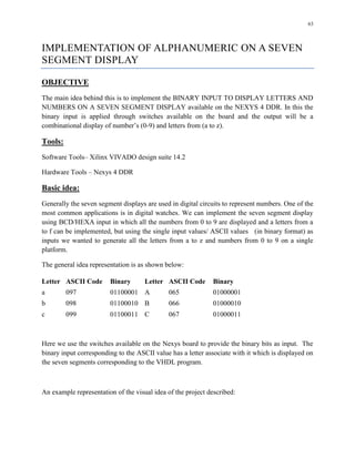
- 1. 63 IMPLEMENTATION OF ALPHANUMERIC ON A SEVEN SEGMENT DISPLAY OBJECTIVE The main idea behind this is to implement the BINARY INPUT TO DISPLAY LETTERS AND NUMBERS ON A SEVEN SEGMENT DISPLAY available on the NEXYS 4 DDR. In this the binary input is applied through switches available on the board and the output will be a combinational display of number’s (0-9) and letters from (a to z). Tools: Software Tools– Xilinx VIVADO design suite 14.2 Hardware Tools – Nexys 4 DDR Basic idea: Generally the seven segment displays are used in digital circuits to represent numbers. One of the most common applications is in digital watches. We can implement the seven segment display using BCD/HEXA input in which all the numbers from 0 to 9 are displayed and a letters from a to f can be implemented, but using the single input values/ ASCII values (in binary format) as inputs we wanted to generate all the letters from a to z and numbers from 0 to 9 on a single platform. The general idea representation is as shown below: Letter ASCII Code Binary Letter ASCII Code Binary a 097 01100001 A 065 01000001 b 098 01100010 B 066 01000010 c 099 01100011 C 067 01000011 Here we use the switches available on the Nexys board to provide the binary bits as input. The binary input corresponding to the ASCII value has a letter associate with it which is displayed on the seven segments corresponding to the VHDL program. An example representation of the visual idea of the project described:
- 2. 64 Block diagram Fig.1 Block Diagram for Alpha Numeric on Seven Segment. Seven Segment Display A seven segment display is a form of electronic display device which is used to display numerals. We can commonly find the seven segment display in digital devices which is used to represent the numeric information to user, like watches, calculators, electronic instruments etc. The name seven segment display itself states that it is a combination of seven segments of display which are arranged in a fashion to represent numerals, when programmed in different fashion. These seven different segments are marked from A-G as in, fig (2). Fig 2: A Generalized Seven Segment Display. FPGA Hardware Kit 6 5 4 3 2 1 0 Switches s Input ASCII Code Simulation & Synthesis in Vivado 14.2 Simulated Waveform Seven segment array Output Seven Segment Display
- 3. 65 Types of seven segment display: There are two types of seven segment display namely 1) Common Anode 7-segment display 2) Common Cathode 7-segment display Display of Numerals &Letters All the numerals can be displayed on the seven segment display. Along with the displaying of numerals we can also display all the alphabets on the seven segments. A series of seven segments display can also be used to represent words and scrolling sentences. The different display of letters can be seen in the fig (2). Fig 2: Seven segment display of letters and numerals The project gives a basic idea of how the seven segment display is used to implement the display of numerals and letters using 8 bits of binary input, using the NEXYS 4 DDR FPGA kit. We have used VHDL coding to program the FPGA [XC100tcsg1] so that the binary input given through switches is decoded according to the program which consists of defined modules to convert the binary input to corresponding seven segment output. According to the program output the seven segments glow to represent the corresponding output.
- 4. 66 In the project we have used a common anode type Seven segment display, hence to make a segment ‘ON’ we have to provide logic ‘0’ and to make a segment ‘OFF’ we have to provide logic ‘1’. Binary Switch Logic INPUTS Fig.3 Segment and switch number representation 1 1 1 1 1 1 1 0 0 0 0 0 0 0 SWITCH ON SWITCH OFF sw1 sw2 sw3 sw4 sw5 sw6 sw7
- 5. 67 Aim: To program the FPGA [XC100tcsg1] in VHDL for display numerals and letters on the seven segments by providing 8 bit binary as input and to verify the output using the hardware kit. Apparatus: Hardware: Nexys 4 DDR FPGA kit. Software: Xilinx Vivado design suite 14.2. Verilog code: module binary_to_seven_segment_display_project( input [6:0] ip, output a,b,c,d,e,f,g, output [7:0] an ); reg a,b,c,d,e,f,g; reg [7:0] an = 8'b11111110; always @ (ip) // checks for every change in input // Code for Alphabets if(ip[5] && ip[6]) begin if(ip[0] && ~ip[1] && ~ip[2] && ~ip[3] && ~ip[4]) begin: a1 a=1'b0; b=1'b0; c=1'b0; d=1'b0; e=1'b0; f=1'b1; g=1'b0; end else if(~ip[0] &&ip[1] && ~ip[2] && ~ip[3] && ~ip[4]) begin : b1 a=1'b1; b=1'b1; c=1'b0; d=1'b0; e=1'b0; f=1'b0; g=1'b0; end else if(ip[0] &&ip[1] && ~ip[2] && ~ip[3] && ~ip[4]) begin: c1 a=1'b1; b=1'b1; c=1'b1; d=1'b0; e=1'b0; f=1'b1; g=1'b0; end else if(~ip[0] && ~ip[1] &&ip[2] && ~ip[3] && ~ip[4]) begin: d1 a=1'b1; b=1'b0; c=1'b0; d=1'b0; e=1'b0; f=1'b1; g=1'b0; end
- 6. 68 else if(ip[0] && ~ip[1] &&ip[2] && ~ip[3] && ~ip[4]) begin: e1 a=1'b0; b=1'b0; c=1'b1; d=1'b0; e=1'b0; f=1'b0; g=1'b0; end else if(~ip[0] &&ip[1] &&ip[2] && ~ip[3] && ~ip[4]) begin: f1 a=1'b0; b=1'b1; c=1'b1; d=1'b1; e=1'b0; f=1'b0; g=1'b0; end else if(ip[0] &&ip[1] &&ip[2] && ~ip[3] && ~ip[4]) begin: g1 a=1'b0; b=1'b0; c=1'b0; d=1'b0; e=1'b1; f=1'b0; g=1'b0; end else if(~ip[0] && ~ip[1] && ~ip[2] &&ip[3] && ~ip[4]) begin: h a=1'b1; b=1'b1; c=1'b0; d=1'b1; e=1'b0; f=1'b0; g=1'b0; end else if(ip[0] && ~ip[1] && ~ip[2] &&ip[3] && ~ip[4]) begin: i a=1'b1; b=1'b1; c=1'b1; d=1'b1; e=1'b0; f=1'b0; g=1'b1; end else if(~ip[0] &&ip[1] && ~ip[2] &&ip[3] && ~ip[4]) begin: j a=1'b1; b=1'b0; c=1'b0; d=1'b0; e=1'b0; f=1'b1; g=1'b1; end else if(ip[0] &&ip[1] && ~ip[2] &&ip[3] && ~ip[4]) begin: k a=1'b1; b=1'b0; c=1'b0; d=1'b1; e=1'b0; f=1'b0; g=1'b0; end else if(~ip[0] && ~ip[1] &&ip[2] &&ip[3] && ~ip[4]) begin: l a=1'b1; b=1'b0; c=1'b0; d=1'b1; e=1'b1; f=1'b1; g=1'b1; end else if(ip[0] && ~ip[1] &&ip[2] &&ip[3] && ~ip[4]) begin: m a=1'b0; b=1'b1; c=1'b0; d=1'b1; e=1'b0; f=1'b1; g=1'b1; end else if(~ip[0] &&ip[1] &&ip[2] &&ip[3] && ~ip[4]) begin: n a=1'b1; b=1'b1; c=1'b0; d=1'b1; e=1'b0; f=1'b1; g=1'b0; end else if(ip[0] &&ip[1] &&ip[2] &&ip[3] && ~ip[4]) begin: o a=1'b1; b=1'b1; c=1'b0; d=1'b0; e=1'b0; f=1'b1; g=1'b0; end else if(~ip[0] && ~ip[1] && ~ip[2] && ~ip[3] &&ip[4]) begin: p
- 7. 69 a=1'b0; b=1'b0; c=1'b1; d=1'b1; e=1'b0; f=1'b0; g=1'b0; end else if(ip[0] && ~ip[1] && ~ip[2] && ~ip[3] &&ip[4]) begin: q a=1'b0; b=1'b0; c=1'b0; d=1'b1; e=1'b1; f=1'b0; g=1'b0; end else if(~ip[0] &&ip[1] && ~ip[2] && ~ip[3] &&ip[4]) begin: r a=1'b1; b=1'b1; c=1'b1; d=1'b1; e=1'b0; f=1'b1; g=1'b0; end else if(ip[0] &&ip[1] && ~ip[2] && ~ip[3] &&ip[4]) begin: s a=1'b0; b=1'b1; c=1'b0; d=1'b0; e=1'b1; f=1'b0; g=1'b0; end else if(~ip[0] && ~ip[1] &&ip[2] && ~ip[3] &&ip[4]) begin: t a=1'b1; b=1'b1; c=1'b1; d=1'b0; e=1'b0; f=1'b0; g=1'b0; end else if(ip[0] && ~ip[1] &&ip[2] && ~ip[3] &&ip[4]) begin: u a=1'b1; b=1'b1; c=1'b0; d=1'b0; e=1'b0; f=1'b1; g=1'b1; end else if(~ip[0] &&ip[1] &&ip[2] && ~ip[3] &&ip[4]) begin: v a=1'b1; b=1'b0; c=1'b0; d=1'b0; e=1'b0; f=1'b0; g=1'b1; end else if(ip[0] &&ip[1] &&ip[2] && ~ip[3] &&ip[4]) begin: w a=1'b1; b=1'b0; c=1'b1; d=1'b0; e=1'b1; f=1'b0; g=1'b1; end else if(~ip[0] && ~ip[1] && ~ip[2] &&ip[3] &&ip[4]) begin: x a=1'b1; b=1'b0; c=1'b0; d=1'b1; e=1'b0; f=1'b0; g=1'b0; end else if(ip[0] && ~ip[1] && ~ip[2] &&ip[3] &&ip[4]) begin: y a=1'b1; b=1'b0; c=1'b0; d=1'b0; e=1'b1; f=1'b0; g=1'b0; end else if(~ip[0] &&ip[1] && ~ip[2] &&ip[3] &&ip[4]) begin: z a=1'b0; b=1'b0; c=1'b1; d=1'b0; e=1'b0; f=1'b1; g=1'b0; end end else
- 8. 70 begin: numbers if(~ip[5] && ~ip[6]) // Code for Numbers begin if(~ip[0] && ~ip[1] && ~ip[2] && ~ip[3] && ~ip[4]) begin: zero a=1'b0; b=1'b0; c=1'b0; d=1'b0; e=1'b0; f=1'b0; g=1'b1; end else if(ip[0] && ~ip[1] && ~ip[2] && ~ip[3] && ~ip[4]) begin: one a=1'b1; b=1'b0; c=1'b0; d=1'b1; e=1'b1; f=1'b1; g=1'b1; end else if(~ip[0] &&ip[1] && ~ip[2] && ~ip[3] && ~ip[4]) begin: two a=1'b0; b=1'b0; c=1'b1; d=1'b0; e=1'b0; f=1'b1; g=1'b0; end else if(ip[0] &&ip[1] && ~ip[2] && ~ip[3] && ~ip[4]) begin: three a=1'b0; b=1'b0; c=1'b0; d=1'b0; e=1'b1; f=1'b1; g=1'b0; end else if(~ip[0] && ~ip[1] &&ip[2] && ~ip[3] && ~ip[4]) begin: four a=1'b1; b=1'b0; c=1'b0; d=1'b1; e=1'b1; f=1'b0; g=1'b0; end else if(ip[0] && ~ip[1] &&ip[2] && ~ip[3] && ~ip[4]) begin: five a=1'b0; b=1'b1; c=1'b0; d=1'b0; e=1'b1; f=1'b0; g=1'b0; end else if(~ip[0] &&ip[1] &&ip[2] && ~ip[3] && ~ip[4]) begin: six a=1'b0; b=1'b1; c=1'b0; d=1'b0; e=1'b0; f=1'b0; g=1'b0; end else if(ip[0] &&ip[1] &&ip[2] && ~ip[3] && ~ip[4]) begin: seven a=1'b0; b=1'b0; c=1'b0; d=1'b1; e=1'b1; f=1'b1; g=1'b1; end else if(~ip[0] && ~ip[1] && ~ip[2] &&ip[3] && ~ip[4]) begin: eight a=1'b0; b=1'b0; c=1'b0; d=1'b0; e=1'b0; f=1'b0; g=1'b0; end else if(ip[0] && ~ip[1] && ~ip[2] &&ip[3] && ~ip[4])
- 9. 71 begin: nine a=1'b0; b=1'b0; c=1'b0; d=1'b1; e=1'b1; f=1'b0; g=1'b0; end else begin: null a=1'b1; b=1'b1; c=1'b1; d=1'b1; e=1'b1; f=1'b1; g=1'b1; end end else begin =1'b1; b=1'b1; c=1'b1; d=1'b1; e=1'b1; f=1'b1; g=1'b1; end end endmodule
- 10. 72 Verification: Simulation: The process of verification of functional correctness of the written code is called simulation The above code is simulated and verified in the Xilinx Vivado design suite 14.2 for the exact output. It needs an additional test bench to be written for the purpose of verification in which we predefine the values. Synthesis: The process of mapping the implemented code onto a real world device is known as synthesis. This is again done by the software After the functional verification we have dumped the code into the hardware kit, Nexys 4 DDR to verify the results on the seven segment display available on the kit Output The result of the above written code is as shown below: Simulated output:
- 11. 73 Synthesized output When i/p is 1001010 output represented as J When i/p is 01100001 output represented as a When i/p is 0000000 output represented as 0 When i/p is 0000111output represented as 7
- 12. 74 Drawbacks: In the above seven segmented display we cannot display few letters accurately for user understanding, the user has to compromise between some letters such as W,X,K etc. Conclusion: The implementation of ASCII code to alphanumeric seven segment display has been performed in the Vivado design suite and the simulated output is verified. The Synthesized output has been performed and observed on the Xilinx Nexys 4 DDR FPGA kit and the sample kit picture has been added to the project report.
- 13. 75