Self test - 2
•
0 likes•147 views

Lorenzo Electronics' System Board self test using Boundary Scan Test and In-Circuit Test technologies

Recommended
More Related Content
What's hot
What's hot (18)
Viewers also liked
Viewers also liked (13)
Similar to Self test - 2
Similar to Self test - 2 (20)
More from Mark Chien
Recently uploaded
Recently uploaded (20)
Self test - 2
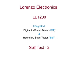
- 1. Lorenzo Electronics LE1200 Integrated Digital In-Circuit Tester (ICT) & Boundary Scan Tester (BST) Self Test - 2
- 2. Scope ● This test enhanced the original LE1200 System Board self tests with additional test points and more test features. ● BST simultaneously test 2 boundary scan devices instead of just 1 in earlier version. ● Fault insertion test with test trace files to attest LE1200 fault detection capabilities.
- 3. Test Setup ● System Board configuration – ICT circuits related to U1, U2, and ICT tester pins 1-128 are converted into BST device under test (DUT) while tester pins 129 - 256 are still functioning as ICT tester (P.4). ● 2 additional jumper wires are added to connect ICT pin 57 to pin 141, and ICT pin 58 to pin 142 (P.5). ● DUT equivalent circuits are shown in P.6.
- 4. DUT ICT Tester U1/U2 JTAG port U1 U2 U3 U4 System Board
- 5. Jumper Wires 23058010374339 ICT pin 141 is wired to pin 57 ICT pin 142 is wired to pin 58 ICT pins 57 and 58, after receiving JTAG test command, will be connected to U1 BSC cells port 84 and 83, respectively.
- 6. BSC ports ICT DUT DUT Equivalent Circuit
- 7. Running Self Test ● This LE1200 Self Test extends the previous Self Test with 2 additional ICT tester pins and 2 ports within BSC device U1. New test patterns are affixed to those of the previous self test. ● Tests will be executed with or without the fault inserted. Excerpts of test trace files from both tests will be illustrated. ● This test is designed to detect Boundary Scan IC pin-short and pin-open defects.
- 8. Test Patterns ● Each test is divided into 2 groups. The 1st group, test pattern 1-23, selected U1/U2 BSC output cells will drive the circuits while their input cells and digital ICT pins 129-136, 141- 142 will be on the receiving end . ● 2nd test group, test pattern 24-42, digital ICT pins 129-136, 141-142 will drive the circuits and U1/U2 BSC input cells will be the receivers. Throughout this test group, U1/U2 BSC output cells are set to Hi-Z states.
- 9. Test Group 1 – U1 ports Driving Tests ● In test pattern 1, U1 pins output cells are reset to 0. Their input cells expected logic states are set to 'X'. ● In the follow on test patterns with alternating ICT/BST test operations, ICT pins 142-141 will validate the logic states driven by U1 port 83-84 output cells setup by the preceding BST test patterns (2-bit up-counter). ● BST test patterns for U1 input cells will validate the logic states driven by the associated output cells setup in the preceding BST test patterns.
- 10. Test Group 2 - ICT Driving Tests ● This test group will start with test pattern #24, which is a BST, by setting U1 ports 83-84 input cells to 'X' state and their output cells to Hi-Z states. ● Test pattern #25 will setup ICT pins 141-142 to drive the inverting 0/1 bit patterns. ● In the follow on test patterns with alternating BST-ICT test operations, BST will validate U1 port 84-83 input cell data against the preceding ICT driving data of inverting 0/1 bit patterns.
- 11. Self Test Trace files ● Excerpts of the trace files, depicted in P.12-14, include (1) sysout text file (2) sysout test pattern CSV file (3) BSC device U1 test pattern CSV file. ● LE1200 test pattern CSV files conventions are that signals driving into DUT are listed as 0/1/Z, and the signals received from DUT are L/H/X.
- 12. Sysout text file
- 13. Sysout – CSV file
- 14. BSC device (U1) CSV file
- 15. Failed Self Test (1) ● Ground wire will be attached to ICT pin #142 and repeat the previous tests. Trace files excerpts are depicted on P.17-19. ● P.17, TDO stream with highlighted nibble 9 instead of nibble d in P.12 => U1 cell #321 is 0. ● P.18, ICT pin d142 detected logic L (failed) in test patterns 6, 8, 14, 16. They failed due to mismatch with logic 1 driven by U1 port IO_P83 output cells in test patterns 5, 7, 13, and 15 (P.18).
- 16. Failed Self Test (2) ● P.19, U1 port IO_P83 input cell detects logic 1 (H) in test patterns 7, 9, 15, and 17, driven by its output cell in test patterns 5, 7, 13, and 15. The injected GND fault is isolated by the buffer circuit and not to affect the input cell. ● P.19, U1 port IO_P83 input cell detects logic 0 (L, failed) in test pattern #28. Test programming expects the port to receive logic 1 driven by ICT pin #142 in pattern 27 (P.18).
- 17. Sysout (failed) – test pattern 28
- 18. Sysout (CSV)
- 19. BSC device (U1) test patterns