SlideShare a Scribd company logo
1 of 21
Download to read offline
© Semiconductor Components Industries, LLC, 2014
May, 2014 − Rev. 2
1 Publication Order Number:
NCP1032/D
NCP1032
Low Power PWM Controller
with On-Chip Power Switch
and Startup Circuits for
Telecom Systems
The NCP1032 is a miniature high−voltage monolithic switching
converter with on−chip power switch and startup circuits. It
incorporates in a single IC all the active power control logic and
protection circuitry required to implement, with minimal external
components several switching regulator applications, such as a
secondary side bias supply or a low power DC−DC converter. This
converter is ideally suited for 24 V and 48 V telecom and medical
isolated power supply applications. The NCP1032 can be configured
in any single−ended topology such as forward or flyback converter.
The NCP1032 is targeted for applications requiring up to 3 W.
The internal error amplifier allows the NCP1032 to be easily
configured for secondary or primary side regulation operation in
isolated and non−isolated configurations. The fixed frequency
oscillator is optimized for operation up to 1 MHz and is capable of
external frequency synchronization, providing additional design
flexibility. In addition, the NCP1032 incorporates undervoltage and
overvoltage line detectors, programmable cycle−by−cycle current
limit, internal soft−start, and thermal shutdown to protect the
controller under fault conditions.
Features
• On Chip High 200 V Power Switch Circuit and Startup Circuit
• Internal Startup Regulator with Auxiliary Winding Override
• Programmable Oscillator Frequency Operation up to 1 MHz
• External Frequency Synchronization Capability
• Frequency Fold−down Under Fault Conditions
• Trimmed ± 2% Internal Reference
• Programmable Cycle−by−Cycle Current Limit
• Internal Soft−Start
• Active Leading Edge Blanking Circuit
• Line Under and Over Voltage Protection
• Over Temperature Protection
• These are Pb−Free Devices
Typical Applications
• POE (Power Over Ethernet)/PD. Refer to Application Note AND8247
• Secondary Side Bias Supply for Isolated DC−DC Converters
• Stand Alone Low Power DC−DC Converter
• Low Power Bias Supply
• Low Power Boost Converter
• Medical Isolated Power Supplies
• Bias Supply for Telecom Systems. Refer to App Note AND8119/D
http://onsemi.com
MARKING
DIAGRAMS
1032 = Specific Device Marking
x = A or B
A = Assembly Location
L = Wafer Lot
Y = Year
W = Work Week
G = Pb−Free Package
PIN CONNECTIONS
(Note: Microdot may be in either location)
See detailed ordering and shipping information in the package
dimensions section on page 20 of this data sheet.
ORDERING INFORMATION
WDFN8
MN SUFFIX
CASE 511BH
1032x
ALYW G
G
ÇÇ
ÇÇ
ÇÇ
ÇÇ
Ç
Ç
Ç
Ç
WDFN8 (Top View)
GND
GND
CT
VFB
COMP
VCC
VDRAIN
CL
UV/OV
1
NCP1032
http://onsemi.com
2
Figure 1. Typical Application – Dual Output Auxiliary Regulated Isolated Flyback
D1
D2
COUT
CVCC
Cin
R3
R4 RCL
CCT
CC RC
CP R1
R2
NCP 1032
VDRAIN
VCC
CL
COMP
VFBGND
CT
UV/OV
VIN VOUT
2.2 mF 22 mF
2.2 mF
Figure 2. NCP1032 Simplified Block Diagram
I1
3.0 V/
3.5 V
S R
PWM
COMP
NCL
NSS
30 ns
One Shot
−
+
2.5 V
Error
Amplifier
−
+
−
+
5.7 V
−
+
−
+
UV
Comp
OV
Comp
2.24 V
I2
Duty
LEB
ISET
FB
COMP
OV/UV
7.6 V
10.2 V
Fault
Logic
NUVLO
NLOWVCC
HIVCC
NUVLO
NLOWVCC
HIVCC
IN1
IN2
IN3
IN4
UVBAR
UVBAR
NUV OUT2
NUV
NOV
NOV
IN5
IN6
nstart
Fault
Fault
Fault
LEBOUT
LEBOUT
Current
Limit
SS
IN7Thermal Trip
12.5 mA
PGND VDRAIN
OUT3
Driver
RT
UVBAR
Internal Bias
nstart
VCC
Internal Bias
Internal Bias
(all pins except VDRAIN pin are protected by 10 V ESD diodes)
Cycle
= 75%
Delay
2 kW
2 kW
1.0 V
2 kW
2 kW
2 kW
3.5 V
150 kW
2 kW
6.6 V
Q
SETCLR
Q
NCP1032
http://onsemi.com
3
Table 1. FUNCTIONAL PIN DESCRIPTION
Pin Name Function Description
1 GND IC Ground Ground reference pin for the circuit.
2 CT Oscillator Frequency
Selection
An external capacitor connected to this pin sets the oscillator frequency up to 1 MHz. The
oscillator can be synchronized to a higher frequency by charging or discharging CT to trip the
internal 3.0 V/3.5 V comparators. If a fault condition exists, the power switch is disabled and
the frequency is reduced.
3 VFB Feedback Signal Input The regulated voltage is scaled down to 2.5 V by means of a resistor divider. Regulation is
achieved by comparing the scaled voltage to an internal 2.5 V reference.
4 COMP Error Amplifier
Compensation
The output of the internal error amplifier. External compensation network between COMP
and VFB pin is required for stable operation.
5 CL Current Limit Threshold
Selection
A resistor RCL connected between this pin and ground sets the peak current value of the
current limit. If the CL pin is left open, the current limit value is set to its initial maximum value
of approximately 12 mA (CLIM_MAX). Programmable current limit threshold, together with
internal soft−start feature effectively limits the primary transformer high current peaks during
startup phase.
6 UV/OV Input Line Undervoltage
and Overvoltage
Shutdown
Input line voltage is scaled down using an external resistor divider. The minimum operating
Vin voltage is achieved when the voltage on UV/OV pin reaches UV threshold 1.0 V. The
maximum operating voltage is then limited by 2.4 V on UV/OV pin. A device version without
OV protection feature is available, see ordering information section.
7 VCC Powers the Internal
Circuitry
Supplies power to the internal control circuitry. Connect an external capacitor for energy
storage during startup. The Vcc voltage should not exceed 16 V during operation.
8 VDRAIN Drain Connection Connects the power switch and startup circuit to the primary transformer windings.
EP EP Thermal Flag This is the thermal flag for the IC and should be soldered to the ground plane.
Table 2. MAXIMUM RATINGS
Rating Symbol Value Unit
Power Switch and Startup Circuits Voltage BVdss −0.3 to +200 V
VCC Power Supply Voltage VCC −0.3 to +16 V
Power Supply Voltage on all Pins, except VDRAIN and VCC VIO −0.3 to +10 V
Drain Current Peak During Transformer Saturation IDS(pk) 1.0 A
Thermal Resistance Junction−to−Air –W DFN8 3x3, case 511BH
(100 sq mm, 2oz) (Note 4)
(500 sq mm, 2oz) (Note 4)
(100 sq mm,2oz,) (Note 5)
RqJA
109
64
44
°C/W
Maximum Junction Temperature TJMAX 150 °C
Storage Temperature Range TSTG −60 to +150 °C
ESD Capability, Human Body Model Pins 1−7 (Note 1) 4.0 kV
ESD Capability, Machine Model Pins 1−7 (Note 1) 400 V
Pin 8 is connected to the high voltage startup and power switch which is protected to
the maximum drain voltage
200 V
Stresses exceeding those listed in the Maximum Ratings table may damage the device. If any of these limits are exceeded, device functionality
should not be assumed, damage may occur and reliability may be affected.
1. This device series contains ESD protection and passes the following tests:
Human Body Model (HBM) ± 2.0 kV per JEDEC standard: JESD22−A114.
Machine Model (MM) ± 200 V per JEDEC standard: JESD22−A115.
2. This device contains latch−up protection and it exceeds ± 100 mA per JEDEC standard: JESD78 class II
3. Moisture Sensitivity Level (MSL): 1 per IPC/JEDEC standard: J−STD−020A
4. EIA JEDEC 51.3, single layer PCB with added heat spreader
5. EIA JEDEC 51.7, four layer PCB with added heat spreader
NCP1032
http://onsemi.com
4
Table 3. ELECTRICAL CHARACTERISTICS
(For typical values Tj = 25°C, for min/max values Tj = −40°C to +125°C, VDRAIN = 48 V, VCC = 12 V, unless otherwise noted)
Symbol Parameter Conditions Min Typ Max Unit
SUPPLY SECTION AND VCC MANAGEMENT
VCC_ON Vcc Voltage at Which the Switcher
Starts Operation
VCC Increasing 9.9 10.2 10.5 V
VCC_MIN Minimum Operating VCC After Turn on
at Which HV Current Source Restarts
VCC Decreasing 7.40 7.55 7.7 V
VCC_RST Vcc Undervoltage Lockout Voltage VCC Decreasing, VFB = VCOMP 6.75 6.95 7.15 V
ICC1 Internal IC Consumption
Power Switch Enabled
MOSFET is switching at 300 kHz 2.0 2.9 4.0 mA
ICC2 Internal IC Consumption
Power Switch Disabled
No Fault condition, VFB = 2.7 V − 2.0 2.5 mA
ICC3 Internal IC Consumption
Power Switch Disabled
Fault condition,
VFB = 2.7 V, VUV/OV < 1.0 V
− 0.75 1.5 mA
POWER SWITCH CIRCUIT
RDSON Power Switch Circuit On−State
Resistance
ID = 100 mA
TJ = 25°C
TJ = 125°C
−
−
4.2
4.9
5.1
8.0
W
BVdss Power Switch Circuit and Startup
Breakdown Voltage
IDS_OFF = 100 mA, VUV_OV < 1.0 V
Tj = 25°C
200 − − V
IDS_OFF Power Switch Circuit and Startup
Circuit Off−State Leakage Current
VDRAIN = 200 V, VUV_OV < 1.0 V
TJ = 25°C
TJ = −40°C to 125°C
−
−
20
20
25
30
mA
tR Switching Characteristics − Rise Time VDS = 48 V, RL = 480 W, Time
(10%−90%)
− 7 − ns
tf Switching Characteristics − Fall Time VDS = 48 V, RL = 480 W, Time
(90%−10%)
− 10 − ns
INTERNAL STARTUP CURRENT SOURCE
ISTART1 HV Current Source Vcc = 0 V,
Tj = 25°C
Tj = −40°C to 125°C
10.0
9.0
12.0
−
14.0
15.0
mA
ISTART2 HV Current Source Vcc = VCC_ON − 0.2 V
Tj = 25°C
Tj = −40°C to 125°C
9.0
8.0
11.0
−
13.0
16.0
mA
Vstart_min Minimum Startup Voltage ISTART2 = 0.5 mA,
Vcc = VCC_ON − 0.2 V, Tj = 25°C − 16.3 −
V
ERROR AMPLIFIER
VREF Reference Voltage VCOMP = VFB, Follower Mode
TJ = 25°C
TJ = −40°C to 125°C
2.45
2.40
2.5
2.5
2.55
2.60
V
REGLINE Line Regulation VCC = 8 V to 16 V, TJ = 25°C − 1.0 3.0 mV
IVFB Input Bias Current VFB = 2.3 V − 70 150 nA
ISRC COMP Source Current VFB = 2.3 V 80 95 125 mA
ISNK COMP Sink Current VFB = 2.7 V 500 700 900 mA
VC_MAX COMP Maximum Voltage ISRC = 0 mA, VFB = 2.3 V 3.95 4.17 4.5 V
VC_MIN COMP Minimum Voltage ISNK = 0 mA, VFB = 2.7 V − 91 200 mV
AVOL Open Loop Voltage Gain (Note 6) − 80 − dB
GBW Gain Bandwidth Product (Note 6) − 1.0 − MHz
NCP1032
http://onsemi.com
5
Table 3. ELECTRICAL CHARACTERISTICS
(For typical values Tj = 25°C, for min/max values Tj = −40°C to +125°C, VDRAIN = 48 V, VCC = 12 V, unless otherwise noted)
Symbol UnitMaxTypMinConditionsParameter
CURRENT LIMIT AND PWM COMPARATOR
CLIM_MAX Max Current Limit Threshold CL pin Floating, TJ = 25°C,
(di/dt = 0.5 A/ms) 420 512 600
mA
CLIM_MIN Min Current Limit Threshold RCL = 20 kW, TJ = 25°C,
(di/dt = 0.1 A/ms) − 57 −
mA
TPLH Propagation Delay from Current Limit Detection to the
Drain OFF State (Note 6)
− 100 − ns
TON_MIN Min On Time Pulse Width FSW = 300 kHz (Note 6) − 240 − ns
Tss Soft−Start Duration (Note 6) − 2.0 − ms
LINE UNDER/OVERVOLTAGE PROTECTIONS
Vuv Undervoltage Lockout Threshold VFB = VCOMP, Vin decreasing 0.95 1.067 1.18 V
VUV_hys Undervoltage Lockout Hysteresis − 70 − mV
Iuv Input Bias Current VFB = 2.3 V − 0 1 mA
VOV Overvoltage Lockout Threshold VFB = VCOMP, Vin increasing (Note 7) 2.3 2.41 2.5 V
Vov_hys Overvoltage Lockout Hysteresis − 158 − mV
TEMPERATURE MANAGEMENT
TSD Thermal Shutdown (Note 6) 175 °C
Hysteresis in Shutdown (Note 6) 20 °C
INTERNAL OSCILLATOR
fOSC1 Oscillation Frequency, 300 kHz CT = 560 pF (Note 9)
TJ = 25°C
TJ = −40°C to 125°C
275
270
300
−
325
335
kHz
fOSC2 Oscillation Frequency, 960 kHz CT = 100 pF, TJ = 25°C − 960 − kHz
ICT_C Timing Charge Current VCT = 3.25 V − 172 − mA
ICT_D Timing Discharge Current VCT = 3.25 V 517 mA
VR_pk Oscillator Ramp Peak Voltage − 3.492 − V
VR_VLY Oscillator Ramp Valley − 2.992 − V
DCMAx Maximum Duty Cycle 70 76.5 80 %
Product parametric performance is indicated in the Electrical Characteristics for the listed test conditions, unless otherwise noted. Product
performance may not be indicated by the Electrical Characteristics if operated under different conditions.
6. Guaranteed by design and characterized
7. The OV/UV option is disabled on the NCP1032B version
8. Oscillator frequency can be externally synchronized to the maximum frequency of the device
NCP1032
http://onsemi.com
6
TYPICAL OPERATING CHARACTERISTICS – Dual Output Isolated Flyback Converter
Figure 3. Efficiency vs. IOUT at VIN = 24, 36, 48
and 72 V, T1 = CoilCraft B0226−EL
Figure 4. VCC Pin Load Regulation at VIN = 24,
36, 48 and 72 V
IOUT (mA) IOUT (mA)
2001751501007550250
0
10
20
30
50
60
70
80
2001751501007550250
12.060
12.065
12.070
12.075
12.080
12.090
12.095
12.100
Figure 5. Startup Sequence, RCL Open, Output
Load = 80 W (IOUT = 150 mA), 1 VCC 3.0 V/
div DC, 2 VOUT 3.0 V/div DC, 3 VIN 10.0 V/
div DC, 4 IPRI 100 mA/div DC, T = 20 ms/div
Figure 6. Soft−Start, RCL open, Output No
Load 1 VCC 3.0 V/div DC, 2 VOUT 3.0 V/div DC,
3 VIN 10.0 V/div DC, 4 IPRI 100 mA/div DC,
T = 500 ms/div
Figure 7. Soft−Start, RCL = 32 kW (CLIM =
250 mA), Output Load = 240 W (IOUT = 50 mA),
1 VCC 3.0 V/div DC, 2 VOUT 3.0 V/div DC, 3 VIN
10.0 V/div DC, 4 IPRI 100 mA/div DC,
T = 1.0 ms/div
Figure 8. Discontinuous Conduction Mode
(DCM), IOUT = 150 mA, 2 VDRAIN 20 V/div DC,
3 ISEC 30 mA/div DC, 4 IPRI 100 mA/div, DC,
T = 500 ns/div
EFFICIENCY(%)
VOUT(V)
125 225
40
36 V
48 V
72 V
24 V
18 V
125 225
12.085
36 V
48 V 72 V
24 V
18 V
NCP1032
http://onsemi.com
7
TYPICAL OPERATING CHARACTERISTICS
Figure 9. Frequency vs. Timing Capacitor CT
at 255C
Figure 10. Oscillator Frequency vs. Junction
Temperature
CAPACITANCE (pF) AMBIENT TEMPERATURE (°C)
248020001520104056080
50
100
200
400
800
1600
100806040200−20−40
300
400
500
600
800
900
1000
1100
Figure 11. Maximum Duty Ratio vs.
Temperature
Figure 12. Maximum Duty Ratio vs. VCC
Voltage
AMBIENT TEMPERATURE (°C) VCC (V)
100806040200−20−40
74.0
74.2
74.6
74.8
75.0
75.4
75.8
76.0
15141312111098
74.0
74.3
74.6
74.9
75.2
75.5
Figure 13. Minimum On Time vs. VCC Figure 14. Power Switch Circuit and Startup
Circuit Leakage Current vs. Drain Voltage
VCC (V) DRAIN VOLTAGE (V)
15141312111098
100
120
160
180
220
240
280
300
24020016012080400
0
4
8
12
16
20
28
30
FREQUENCY(kHz)
SWITCHINGFREQUENCY(kHz)
DUTYCYCLE(%)
DUTYCYCLE(%)
MINONTIME(ns)
IDS(off),POWERSWITCHANDSTARTUP
CIRCUITSLEAKAGECURRENT(mA)
120
700
CT = 82 pF
CT = 220 pF
CT = 560 pF
120
74.4
75.2
75.6 1.04 MHz
597 kHz320 kHz
128 kHz
16
VDRAIN = 100 V
VDRAIN = 48 V
VDRAIN = 15 V
16
140
200
260
VDRAIN = 100 V
VDRAIN = 48 V
VDRAIN = 15 V
24
6
10
14
18
22
26
2
125°C
25°C
−40°C
NCP1032
http://onsemi.com
8
TYPICAL OPERATING CHARACTERISTICS
Figure 15. Power Switch RDSON vs. Junction
Temperature
Figure 16. Vdrain Startup Threshold over
Temperature
TJ, JUNCTION TEMPERATURE (°C) TJ, JUNCTION TEMPERATURE (°C)
100806040200−20−40
2.9
3.1
3.5
3.9
4.3
4.7
5.1
5.5
100806040200−20−40
16.10
16.14
16.18
16.22
Figure 17. Startup Current vs. Junction
Temperature
Figure 18. Undervoltage Lockout Threshold
vs. Junction Temperature
TJ, JUNCTION TEMPERATURE (°C) TJ, JUNCTION TEMPERATURE (°C)
100806040200−20−40
10.2
10.4
10.8
11.2
11.6
11.8
12.4
12.8
100806040200−20−40
6.930
6.935
6.940
6.945
6.950
6.955
6.960
6.965
Figure 19. Supply Voltage Thresholds vs.
Junction Temperature
Figure 20. VCC Input Current at 12 V with an
18 V applied Drain voltage 255C VS Oscillator
Frequency
TJ, JUNCTION TEMPERATURE (°C) FREQUENCY (kHz)
100806040200−20−40
7.25
7.50
8.00
8.50
9.00
9.50
10.00
10.50
800700600500400300200100
2.00
2.25
3.00
3.25
3.75
4.25
4.75
5.25
RDS(on),POWERSWITCHON
RESISTANCE(W)
VCC(reset),UNDERVOLTAGE
LOCKOUTTHRESHOLD(V)
ISTART,STARTUPCURRENT(mA)
VCC(reset),UNDERVOLTAGE
LOCKOUTTHRESHOLD(V)
UVTHRESHOLD(V)
INPUTCURRENT(mA)
120
3.3
3.7
4.1
4.5
4.9
5.3
VCC = 16 V
VCC = 12 V
VCC = 8 V
16.12
16.16
16.20
16.24
16.30
16.34
16.38
16.28
16.32
16.36
16.40
16.26
120
120
10.6
11.0
11.4
12.0
12.2
12.6
VCC = VCC(on) − 0.2 V
VCC = 0 V
120
120
7.75
8.25
8.75
9.25
9.75
10.25
Startup Threshold
Minimum Operating Threshold
900 1000
2.50
2.75
3.50
4.00
4.50
5.00
NCP1032
http://onsemi.com
9
TYPICAL OPERATING CHARACTERISTICS
Figure 21. Operating Supply Current vs.
Supply Voltage at 320 kHz
Figure 22. VCC Input Current vs. Temperature
over Frequency span VDrain = 48 V
VCC, SUPPLY VOLTAGE (V) AMBIENT TEMPERATURE (°C)
15141312111098
2.1
2.3
2.7
2.9
3.1
3.5
3.7
4.1
100806040200−20−40
2.0
2.5
3.5
4.0
4.5
5.5
6.0
6.5
Figure 23. COMP Clamp Voltage vs. Junction
Temperature
Figure 24. Reference Voltage vs. Junction
Temperature
TJ, JUNCTION TEMPERATURE (°C) TJ, JUNCTION TEMPERATURE (°C)
100806040200−20−40
4.11
4.12
4.14
4.16
4.18
4.20
4.21
4.23
100806040200−20−40
2.488
2.490
2.491
2.493
2.495
2.496
2.498
2.500
Figure 25. COMP Source Current vs. Junction
Temperature
Figure 26. COMP Sink Current vs. Junction
Temperature
TJ, JUNCTION TEMPERATURE (°C) TJ, JUNCTION TEMPERATURE (°C)
100806040200−20−40
94.00
94.25
94.75
95.00
95.25
95.75
96.00
96.50
100806040200−20−40
620
640
680
700
720
740
780
800
ICC1,OPERATINGSUPPLY
CURRENT(mA)
INPUTCURRENT(mA)
VcCLAMP(V)
REFERENCEVOLTAGE(V)
SOURCECURRENT(mA)
SINKCURRENT(mA)
16
2.5
3.3
3.9 VDRAIN = 48 V
TJ = 25°C
CT = 560 pF
120
3.0
5.0
1.04 MHz
597 kHz
320 kHz
128 kHz
2.489
2.492
2.494
2.497
2.499
120
VCC = 16 V
VCC = 12 VVCC = 8 V
120
94.50
95.50
96.25 VCC = 16 V
VCC = 12 V
VCC = 8 V
120
660
760
120
4.13
4.15
4.17
4.19
4.22
NCP1032
http://onsemi.com
10
TYPICAL OPERATING CHARACTERISTICS
Figure 27. Undervoltage Threshold vs.
Junction Temperature
Figure 28. Overvoltage Threshold vs. Junction
Temperature
TJ, JUNCTION TEMPERATURE (°C) TJ, JUNCTION TEMPERATURE (°C)
100806040200−20−40
1.060
1.061
1.063
1.065
1.067
1.069
1.070
1.072
100806040200−20−40
2.394
Figure 29. Under/Overvoltage Hysteresis vs.
Junction Temperature
Figure 30. Current Limit Threshold vs. RCL,
Current Slew Rate = 0.5 A/ms
TJ, JUNCTION TEMPERATURE (°C) RISET (kW)
100806040200−20−40
60
80
90
110
130
150
160
180
18014012010080604020
50
100
150
200
250
350
400
450
Figure 31. Current Limit Threshold vs. Current
Slew Rate
Figure 32. Current Limit Threshold vs. TJ,
Current Slew RISET = Open = 0.5 A/ms, RISET
= 55 kW = 0.3 A/ms, RISET = 22 kW = 0.1 A/ms
CURRENT SLEW RATE (mA/mS) TJ, JUNCTION TEMPERATURE (°C)
10008007004003002001000
270
280
290
300
310
320
330
340
100806040200−20−40
50
100
200
250
300
400
500
550
UVTHRESHOLD(V)
OVTHRESHOLD(V)
VUV/OV(hys),HYSTERESIS(mV)
ILIM,CURRENTLIMITTHRESHOLD(mA)
VCC = 16 V
VCC = 12 V
VCC = 8 V
120
1.062
1.064
1.066
1.068
1.071 VCC = 16 V
VCC = 12 V
VCC = 8 V
120
2.396
2.398
2.400
2.402
2.404
2.406
2.408
2.410
2.412
2.414
2.416
2.418
2.420
2.422
70
100
120
140
170
120
OV Hysteresis
UV Hysteresis
160 200
300
600500 900
25 V 72 V
120 mH
ILIM,CURRENTLIMITTHRESHOLD(mA)
120
150
350
450
RISET = OPEN
RISET = 50 kW
RISET = 22 kW
NCP1032
http://onsemi.com
11
CT Ramp
CT Charge
Signal
PWM
Comparator
Output
Power Switch
Circuit Gate Drive
PWM Latch
Output
Leading Edge
Blanking Output
Current Limit
Propagation
Current Limit
Threshold
Output OverloadNormal PWM Operating Range
Figure 33. Pulse Width Modulation Timing Diagram
Delay
Output OverloadNormal OperationStartup
Mode
Dynamic
Self Supply
VCC(on)
VCC(off)
VCC(reset)
0 V
ISTART
0 mA
0 V
3.0 V
2.5 V
0 V
0 V
Figure 34. Auxiliary Winding Operation with Output Overload Timing Diagram
VDRAIN
VFB
VUV
NCP1032
http://onsemi.com
12
Introduction
The NCP1032 is a monolithic voltage−mode switching
regulator designed for isolated and non−isolated bias supply
applications. The internal startup circuit and the MOSFET
are rated at 200 V, making them ideal for 24 V through 48 V
telecom and 42 V automotive applications. In addition, the
NCP1032 can operate from an existing 12 V supply. The
regulator is optimized for operation up to 1 MHz.
The NCP1032 device incorporates all of the active power,
control logic, protection circuitry, and power switch in a
single IC. The compact design allows the designer to use
minimal external components on several switching
regulator applications, such as a secondary side bias supply
or a low power DC−DC converter.
The NCP1032 is available in the space saving WDFN8
3 x 3 mm package and is targeted for applications requiring
up to 3 W.
The NCP1032 has an extensive set of features including
programmable cycle−by−cycle current limit, internal
soft−start, input line under and over voltage detection
comparators with hysteresis, regulator output undervoltage
lockout with hysteresis and over temperature protection
providing protection during fault conditions. A description
of each of the functional blocks is given below and the
functional block diagram is shown in Figure 2.
Startup Supply Circuit and Undervoltage Lockout
The NCP1032 contains an internal 200 V startup regulator
that eliminates the need for external startup components.
The startup regulator consists of a 12 mA (typical) current
source that supplies power from the input line (VDRAIN)
pin to charge the capacitor on the VCC pin (CVCC). The act
of charging the CVCC capacitor until it reaches 10.2 V while
holding the power switch off is called Startup Mode (SM).
Once the current source charges the VCC voltage to 10.2 V
(typical) the startup circuit is disabled and if no faults are
present, the power switch circuit is enabled. The internal
control circuitry will draw its current from the energy held
by the CVCC capacitor. The startup regulator turns on again
once VCC reaches 7.55 V. The charging of the CVCC
capacitor to 10.2 V by the current source and the discharging
by the control circuitry to 7.55 V will be henceforth referred
to as Dynamic Self Supply (DSS).
If VCC falls below 7.55 V while switching, the device
enters a Restart Mode (RM). While in the RM the CVCC
capacitor is allowed to discharge to 6.95 V while the power
switch is enabled. Once the 6.95 V threshold is reached, the
power switch circuit is disabled, and the startup regulator is
enabled to charge the CVCC capacitor. The power switch is
enabled again once the VCC voltage reaches 10.2 V.
Therefore, the external CVCC capacitor must be sized such
that a voltage greater than 6.95 V is maintained on the VCC
pin while the converter output reaches regulation. The
output is delayed 0.4 ms (TSS_Delay) from the released
undervoltage lockout to the first switching pulse. The
soft−start time TSS is fixed at 2 ms to ramp the current from
its minimum value to its maximum value. The soft−start
time is load and RCL dependent and can be computed in the
soft−start section. The designer must evaluate the current
draw of the regulator at the desired switching frequency over
the VCC and temperature operating range shown in Figures
20 − 22. CVCC is calculated using the following equation:
CVCC +
ICC
ǒTSS_Delay ) TSS
Ǔ
VCC_ON * VCC_MIN
³
2.95 mF +
4.0 mA ǒ0.4 ms ) 2.0 msǓ
10.2 V * 6.95 V
(eq. 1)
ICC includes the NCP1032 bias current (ICC1_MAX) and
any additional current used to bias the feedback (if used).
Assuming an ICC1_MAX of 3.5 mA plus a 0.5 mA bias
current for the feedback sensing resistors (if used), and Tss
of 2 ms, CVCC is calculated at 2.95 mF and should be rounded
up to ensure design margin to 3.3 mF. Please note that if the
feedback sensing resistors are connected to the VCC pin
(isolated main output topology) and CVCC is increased to
match COUT, the transient response of the converter will
suffer. The poor transient response is due to the imbalanced
capacitance to current ratio. The auxiliary winding has a
significantly greater capacitance to current ratio than the
output winding, taking it longer for CVCC to follow COUT
during a transient condition.
After initial startup, the VCC pin should be biased above
VCC_min using an auxiliary winding. This will prevent the
startup regulator from turning on during normal operation,
reducing device power dissipation. A load should not be
directly connected to the VCC pin. A load greater than
12 mA will override the startup circuit possibly damaging
the part. The maximum voltage rating of the startup circuit
is 200 V. Power dissipation should be observed to avoid
exceeding the maximum power dissipation of the package.
Figure 35 shows the recommended configuration for a
non−isolated flyback converter.
Figure 35. Non−Isolated Bias Supply
Configuration
D1
D2
COUT
CVCC
Cin
R3
R4
RCL
CCT
CC RC
CP
R1
R2
VDRAIN
VCC
CL
COMP
VFB
GND
CT
UV/OV
VIN VOUTT1
Lsec
Lbias
Lpri
NCP1032
NCP1032
http://onsemi.com
13
Soft−Start
The NCP1032 features an internal soft−start which
reduces power−on stress and also contributes to the lower
output overshoot. Once the VCC_ON threshold is reached
and there are no fault conditions, the power switch is enabled
and the cycle−by−cycle current limit is ramped up slowly to
the current limit threshold set by the CL pin. If the CL pin
is open, the current limit will be set to its maximum value
and the soft−start time will be 2 ms as shown in Figure 36.
The equation below can be used to calculate the soft−start
time for all other current limit set values.
TSSR +
SetCurrent * MinCurrent
MaxCurrent * MinCurrent
TSS ³
1.07 ms +
300 mA * 57 mA
512 mA * 57 mA
2 ms
(eq. 2)
COMP Voltage
4.2 V
3.5
3.0 V
PWM Signal
Ramp
Inductor Current
Current Limit
57 mA
Set Limit
Soft−Start Time Correction
Time
Figure 36. Soft−Start Time
The compensation of the converter must be manipulated
to minimize the overshoot of the output voltage during
startup, details are in the compensation section.
Line Under and Over Voltage Detectors
The NCP1032 incorporates Vin input line under voltage
(UV) and over voltage (OV) shutdown circuits. If the
UV/OV pin is set below 1.0 V or above 2.4 V thresholds the
power switch will stop switching and the part will use DSS
until the problem is corrected. The comparators incorporate
typical voltage hysteresis of 70 mV (UV) and 158 mV (OV)
to prevent noise from inadvertently triggering the shutdown
circuit. The UV/OV sense pin can be biased using an
external resistor divider from the input line as shown in
Figure 37. The UV/OV pin should be bypassed using a 1 nF
capacitor to prevent triggering the UV/OV circuit during
normal switching operation.
R3
VIN
1 nF
R4 1 V
2.4 V
OV
Comparator
UV
Comparator
Fault
OV Enable
Figure 37. UV/OV Resistor Divider
from the Input Line
CUV
Logic
The resistive network impedance must not be too high to
keep good voltage accuracy and not too low to minimize
power losses. A 200 kW to 1.2 MW range is recommended
for the high side resistor R3. If the designer wanted to set the
undervoltage threshold to 32 V, the resistor divider should be
designed according to the following equation:
R4 +
VUV R3
VIN_UV * VUV
³
34.49 kW +
1.067 1 MW
32 V * 1.067
[ 34.0 kW (R96 Value)
(eq. 3)
NCP1032
http://onsemi.com
14
The OV threshold monitored at the UV/OV pin is 2.41
times higher than the UV threshold, leading to an OV
threshold of 73.3 V for the calculated R96 value. Designers
can quickly set the OV/UV thresholds by referencing
Figure 38.
Figure 38. UV/OV Resistor Divider Thresholds
with R4 Set to 10 k
R3 (kW)
450400 500350300250200150
10
20
40
50
70
90
100
120
INPUTVOLTAGE(V)
30
60
80
110
Overvoltage Threshold
Undervoltage Threshold
The UV/OV pin can also be used to implement a remote
enable/disable function. If an external transistor pulls the
UV/OV pin below 1.0 V (or above 2.4 V) the converter will
be disabled and no switching is allowed. A device version is
available without the OV protection feature, see the ordering
information section.
Error Amplifier
The internal error amplifier (EA) regulates the output
voltage of the bias supply. The scaled signal is fed into the
feedback pin (VFB) which is the inverting input of the error
amplifier. It compares a scaled voltage signal to an internal
trimmed 2.5 V reference connected to its non−inverting
input.
The output of the error amplifier is internally connected
to a PWM comparator and also available externally through
the COMP pin for frequency compensation. To insure
normal operation, the EA compensation should be selected
such that the EA frequency response crosses 0 dB below
80 kHz.
The error amplifier feedback bias current is less than
200 nA over the operating range. The output source and sink
currents are typically 95 mA and 700 mA, respectively.
Under load transient conditions, COMP may need to
move from the bottom to the top of the CT ramp. A large
current is required to complete the COMP swing if small
resistors or large capacitors are used to implement the
compensation network. In which case, the COMP swing will
be limited by the EA source current. Optimum transient
responses are obtained if the compensation components
allow the COMP pin to swing across its operating range in
1 cycle.
Oscillator, Voltage Feed Forward, and Sync Capability
The oscillator is optimized for operation up to 1 MHz and
its frequency is set by the external timing capacitor (CT)
connected to the CT pin. The oscillator has two modes of
operation: free running and synchronized (sync). While in
free running mode, an internal current source sequentially
charges and discharges CT generating a voltage ramp
between 3.0 V and 3.5 V. Under normal operating
conditions, the charge (ICT_C) and discharge (ICT_D)
currents are typically 172 mA and 515 mA, respectively. The
charge/discharge current ratio of 1:3 discharges CT in 25%
of the total period. The power switch is disabled while CT is
discharging, guaranteeing a maximum duty cycle of 75% as
shown in Figure 39.
25%
75%Signal
Power Switch
Enabled
COMP
Max Duty
Cycle
Figure 39. Auxiliary Winding Operation with
Output Overload Timing Diagram
CT Ramp
CT Charge
The oscillator frequency should be set no more than 25%
below the target sync frequency to maintain an adequate
voltage ramp and provide good noise immunity. A possible
circuit to synchronize the oscillator is shown in Figure 40.
C1
R1 R2
2
Figure 40. External Frequency
Synchronization Circuit
CT
CT
NCP1032
http://onsemi.com
15
Voltage feed forward can be implemented by connecting
a resistor from the input voltage to the CT pin. RFF supplies
a current that allows the input voltage to modify the
maximum duty cycle rather than the standard 75%
maximum. If the designer wanted to implement a fixed
lower duty cycle, a resistor can be tied to a fixed voltage
source such as VAUX or a voltage reference. If voltage feed
forward is used, the frequency can shift dramatically
depending on the value of the resistor.
Cin
RFF
CCT
NCP1032
VDRAIN
GND
CTVIN
Z1
4 V
IFF
2.2 mF
Off
On
Time
Off
Time
On
Time
66%
Off
On
Time
75% 58% 53%
Off
Time
On
Time
42%
Off
Time
On
Time
38%
Off
Time
On
Time
29%
Off
Time
On
21%
Off
Time
On
Feed Forward Voltage
CT PIN Voltage
Figure 41. Voltage Feed Forward
RVFF +
VINMIN * Ramp
ICT_D * DMAX
ǒICT_C ) ICT_D
Ǔ
³
320 kW +
32 V * 3.25 V
517 mA * 62% ǒ172 mA ) 517 mAǓ
(eq. 4)
PWM Comparator and Latch
The Pulse Width Modulator (PWM) comparator
compares the error amplifier output (COMP) to the CT ramp
and generates a proportional duty cycle. The power switch
is disabled while COMP voltage is below the CT ramp
signal. Once COMP reaches the ramp signal, the power
switch is enabled. If COMP is at the bottom of the CT ramp,
the converter operates at minimum duty cycle. While COMP
increases, the duty cycle increases until COMP reaches the
peak of the CT ramp, at which point the controller operates
at maximum duty cycle.
The CT charge signal is filtered through a one shot pulse
generator to set the PWM latch and enable switching at the
beginning of each period. Switching is allowed while the CT
ramp is below COMP and a current limit fault is not present.
The pulse width modulation technique is seen in
Figure 39.
The PWM comparator and latch propagation delay are
less than 200 ns. If the system is designed to operate with a
minimum on time less than 200 ns (no or light load), the
converter will skip pulses. Skipping pulses is usually not a
problem, unless operating at a frequency close to the audible
range. Skipping pulses is more likely when operating at high
frequencies during high input voltage and minimum load
conditions.
A 2 kW series resistor is included for ESD protection
between the internal EA output and the COMP pin. Under
normal operation, a 220 mV offset is observed between the
CT ramp and the COMP crossing points. The series resistor
does not interact with the error amplifier transfer function.
Programmable Current Limit
The power switch circuit incorporates SENSEFET®
technology to monitor the drain current. A sense voltage is
generated bydrivinga sense element, RSENSE, with a current
proportional to the drain current. The sense voltage is
compared to an externally programmable reference voltage
on the non−inverting input of the current limit comparator.
If the sense voltage exceeds the setup reference level, the
comparator resets the PWM latch and the switching cycle is
terminated. The reference level threshold is programmable
by a resistor (RCL) connected to the CL pin shown in
Figure 42.
By limiting the peak current to the needs of the
application, the transformer sizing can be scaled
appropriately to the specific requirements which allows the
PCB footprint to be minimized. The NCP1032 maximum
drain current limit thresholds are 512 mA.
RCL + 114 ln(Rset) * 142 (eq. 5)
RCL + 309 ln(Rset) * 893
Rset t 42.2 kW
200 kW u Rset u 42.2 kW
Current Limit
Comparator
Fault Logic
Sense
MOSFET
DRIVER
Leading Edge
Blanking GND
VDRAIN
100 ns
RCL
Soft−Start Ramp+
+
−
CL
Figure 42. Current Limit Threshold and
Propagation Delay
3.2 mA
NCP1032
http://onsemi.com
16
The propagation delay is measured from the time an
overcurrent fault appears at power switch circuit drain, to the
start of the turn−off transition as shown in Figure 43. The
current limit propagation delay time is typ. 100 ns. The
propagation must be accounted for when designing the
power supply, as it will result in a constant power output
through the transformer when the output is shorted. The
constant power can cause the transformer to rise in
temperature permanently damaging the magnetics. This can
be mitigated by placing a 10 W resistor in series with the
output rectification diode.
t
Figure 43. Current Limit Threshold and
Propagation Delay
ISW
ILIM
TPHL
VIN
LP
TPHL
Adaptive Leading Edge Blanking
Each time the power switch circuit is turned on, a narrow
voltage spike appears across RSENSE. The spike is due to the
power switch circuit gate to source capacitance, transformer
interwinding capacitance, and output rectifier recovery
time. The spike can cause a premature reset of the PWM
latch. A proprietary active Leading Edge Blanking (LEB)
circuit masks the current signal to prevent the voltage spike
from resetting the PWM latch. The active LEB masks the
current signal until the power switch turn on transition is
complete. The adaptive LEB period provides better current
limit control compared to a fixed blanking period.
Power Switch Circuit Protection
The NCP1032 monolithically integrates a 200 V power
switch with control logic circuitry. The power switch is
designed to directly drive the converter transformer. The
gate drive is tailored to control switching transitions and
help limit electromagnetic interference (EMI).
For a Flyback topology a large transient voltage spike
appears at the transformers primary side after the power
switch turns off. These spikes are a function of the
transformer leakage inductance (LLP) on either the primary
or secondary side. A circuit is needed to clamp the leakage
spike, limiting the voltage drain excursion to a safe value.
The operating VDRAIN_MAX is 200 V as depicted in
Figure 44. Two such circuits are the passive RCD network
or a zener clamp as depicted in Figure 45 and Figure 46.
t
Figure 44. Power Switch Waveforms with Clamping
VIN
VCLAMP
VR
VDRAIN
VLS (leakage spike)
VDRAIN_MAX (180 V)
Vin
D_Clamp
Cclamp
−
+
Cin D1
+
Rcl
T1
−
Cvcc
Cout
Rclamp
U?
NCP1032_33
VCC
7
VDRAIN
8
CL 5
VFB
3
COMP 4
GND
1
UV/OV
6
CT
2
Figure 45. Passive RCD Clamp Network
VF
The passive RCD network is the most standard circuitry
and the formula below is used to calculate RCLAMP and
CCLAMP.
RCLAMP +
2 VCLAMP
ǒVCLAMP * (VOUT ) VF) NǓ
LLP IPEAK
2 FSW
CCLAMP +
VCLAMP
VLS FSW RCLAMP
(eq. 6)
NCP1032
http://onsemi.com
17
The voltage leakage spike (VLS) is usually selected 50 to
70% above the reflected value VR = N x (VOUT + VF) and
(VIN + VCLAMP) must be below the operating VDRAIN−MAX
which is 200 V. The diode used for the clamping circuit
needs to be at minimum fast or ultrafast recovery and an
MURA110 represents a good choice. One major drawback
of the RCD network lies in its dependency upon the peak
current. The worse case occurs when IPEAK and VIN are at
the maximum.
Dz_clamp
Vin
D_Clamp
−
+
Cin D1
+
Rcl
T1
−
Cvcc
Cout
U?
NCP1032_33
VCC
7
VDRAIN
8
CL
5
VFB
3
COMP
4
GND
1
UV/OV
6
CT
2
Figure 46. Zener Clamp Network
VF
The zener diode is probably the most expensive but offers
the best protection and a very precise clamping level. Select
the zener voltage to set VLS level between 10 to 15 V above
the reflected voltage VR so VZener = VLS + VR. The zener
diode must be able to handle the voltage rating and power
dissipation during the switch turn−off time. For the
NCP1032, a 0.5 W zener diode, like the MMSZ47T1 is
suitable.
Thermal Shutdown
Internal thermal shutdown circuitry is provided to protect
the integrated circuit in the event that the maximum junction
temperature is exceeded. When activated at 165°C, the
power switch circuit is disabled. Once the junction
temperature falls below 145°C, the NCP1032 is allowed to
resume normal operation. This feature is provided to prevent
catastrophic failures from accidental device overheating. It
is not intended to be used as a substitute for proper heat
sinking.
Application Considerations
Typical Applications
A 12 V / 3 W bias supply for 36 V to 75 V telecom systems,
1500 V isolation DC−DC converters. The NCP1032 is
configured in Flyback topology and operates in
Discontinuous Conduction Mode (DCM) to offer a
low−cost, high efficiency solution. The circuit schematic is
shown in Figure 47. Transformer T1 is available as a
CoilCraft B0226−EL. Capacitor CCT sets the switching
frequency at approximately 300 kHz.
Output voltage regulation and overall efficiency are
shown in Figure 3 and Figure 4 on page 6. The resistor
divider formed by R3 and R4 sets the undervoltage lockout
threshold at about 32 V.
Application Note AND8119/D describes the design of
this bias supply system.
−
+
2.2 mF
Cin
D2
NRVB0540
R2
5.1 K
R1
19.6 K
2.2 mF
Cvcc
D1
MBR140
22 mF
Cout
+
Cc
100 nF
Rc
18 K
Cp 68 pF
R3
1 M
R4
32.4
560 pF
Cct
T1
Lsec
Lpri
Lbias
U1
NCP1032
VCC
7
VDRAIN
8
CL
5
VFB
3
COMP
4
GND
1
UV/OV
6
CT
2
L1 2.2mH
Cclp
1 nF
MBR1H100
Dclp
Rclp
18 k
1000 pF
C1
1 nF
Cuv
−
Figure 47. 48 V to Isolated 12 V / 3 W Bias Supply Schematic
NCP1032
http://onsemi.com
18
Layout Recommendations
To prevent EMI problems high current copper traces
which have high frequency switching should be optimized.
Therefore, use short and wide traces for power current paths
and for power ground traces especially transformer trace
connections (primary and secondary). When power is
transferred from input to output, there is a period of time
when the power switch is on, referred to as “on time,” and
a period of time when the switch is off, referred to as “off
time.” When the power switch is on, the input voltage is
applied across the primary side of the transformer and
current increases in the primary inductance. Further, when
the power switch is on the output current is supplied from the
output capacitance. When the power switch is off, current on
the primary side conducts through the clamp or snubber
circuit. On the secondary side current is conducting through
the rectification diode, providing power to the output and
replenishing energy in the output capacitances as shown in
Figure 48. Electromagnetic radiation is minimized by
keeping VDRAIN leads, output diode, and output bypass
capacitor leads as short as possible. It is important to
minimize the area of the VDRAIN nodes and used the
ground plane under the switcher circuitry to prevent
interplane coupling and minimize cross−talk to sensitive
signals and ICs. The exposed pad of the package must be
connected to the ground plane of the board which is
important for EMI and thermal management. Finally, it is
always good practice to keep sensitive traces such as
feedback connection (VFB and COMP) as far away from
switched signal connections (VDRAIN) as possible.
Figure 48 shows an example of an optimized PCB layout.
Thermal Considerations
Careful attention must be paid to the internal power
dissipation of the NCP1032. Power dissipation is a function
of efficiency and output power. As output power
requirements increase, proper component selection includes
adjusting RDSON, forward voltage of diodes, and enlarging
packages. For example, if a transformer’s size were
increased to lower the DCR or/and increase the inductance
efficiency will improve at heavier loads. The exposed
thermal pad is designed to be soldered to the ground plane
used as a heat sink. The ground plane size should be
maximized and connected to the internal and bottom copper
ground planes with thermal vias placed directly under the
package to spread heat generated by the NCP1032 as
depicted Figure 48.
Figure 48. Recommended PCB Layout
NCP1032
http://onsemi.com
19
−
+
2.2 mF
Cin
R2
20 K
R1
20 K
D1
MBR140SFT1G
22 mF
Cout
+
Cc
100 nF
Rc
18 K
Cp 68 pF
R3
1 M
R4
32.4
560 pF
Cct
Vin 32 to 75 V
LsecLpri
U1
NCP1032
VCC
7
VDRAIN
8
CL
5
VFB
3
COMP
4
GND
1
UV/OV
6
CT
2
Cclp
1 nF
MBR1H100SFT3G
Dclp
Rclp
18 k
1 nF
Cuv
− Vout 5.0 V
600 mA
D4
MMSZ5243BT1G
Q1
NSS1C201LT1G
R7
18 k
T14:1
1.0 mF
Cvcc
Figure 49. 48 V to 5.0 V DC−DC Converter Without Auxiliary Winding
−
+
2.2 mF
Cin
R2
20 K
R1
20 K
D1
MBR140SFT1G
22 mF
Cout
+
Cc
100 nF
Rc
18 K
Cp 68 pF
R3
1 M
R4
32.4
560 pF
Cct
Lpri
Vin 32 to 75 V
Lsec
U1
NCP1032
VCC
7
VDRAIN8
CL
5
VFB
3
COMP
4
GND
1
UV/OV
6
CT
2
Cclp
1 nF
MBR1H100SFT3G
Dclp
Rclp
18 k
1 nF
Cuv
− Vout 12.0 V
300 mA
T13:1
100 nF
Cvcc
Figure 50. 48 V to 12.0 V DC−DC Converter Without Auxiliary Winding
NCP1032
http://onsemi.com
20
D1
MURA115 COUT
22 mF
Cin
1 mF
R3
294 kW
RCL
40.2 kW
CCT
CC 1.5 nF
CP 100 pF
R1
78.7 kW
NCP1032
VDRAIN
VCC
CL
COMP
VFB
GND
CT
UV/OV
VIN VOUT
560 mF
100 V
50 mA
R4
10 kW
R2
2 kW
RC
100 kW
Figure 51. Typical Application Circuit Boost Circuit Configuration
ORDERING INFORMATION
Device OV Protection Marking Package Shipping†
NCP1032AMNTXG Enable 1032A WDFN8 3x3
(Pb−Free)
3,000 / Tape & Reel
NCP1032BMNTXG Disable 1032B WDFN8 3x3
(Pb−Free)
3,000 / Tape & Reel
†For information on tape and reel specifications, including part orientation and tape sizes, please refer to our Tape and Reel Packaging
Specifications Brochure, BRD8011/D.
NCP1032
http://onsemi.com
21
PACKAGE DIMENSIONS
WDFN8 3x3, 0.65P
CASE 511BH
ISSUE O
NOTES:
1. DIMENSIONING AND TOLERANCING PER
ASME Y14.5M, 1994.
2. CONTROLLING DIMENSION: MILLIMETERS.
3. DIMENSION b APPLIES TO PLATED
TERMINAL AND IS MEASURED BETWEEN
0.15 AND 0.30 MM FROM TERMINAL TIP.
4. COPLANARITY APPLIES TO THE EXPOSED
PAD AS WELL AS THE TERMINALS.
ÇÇÇÇ
ÇÇÇÇÇÇÇÇ
AD
E
B
C0.10
PIN ONE
2X
REFERENCE
2X
TOP VIEW
SIDE VIEW
BOTTOM VIEW
L
D2
E2
C
C0.10
C0.10
C0.08
A1
SEATING
PLANE
8X
NOTE 3
b8X
0.10 C
0.05 C
A BB
DIM MIN MAX
MILLIMETERS
A 0.70 0.80
A1 0.00 0.05
b 0.25 0.35
D 3.00 BSC
D2 2.20 2.40
E 3.00 BSC
E2 1.40 1.60
e 0.65 BSC
L 0.20 0.40
1 4
8
*For additional information on our Pb−Free strategy and soldering
details, please download the ON Semiconductor Soldering and
Mounting Techniques Reference Manual, SOLDERRM/D.
SOLDERING FOOTPRINT*
0.65
PITCH
1.66 3.30
1
DIMENSIONS: MILLIMETERS
0.53
8X
NOTE 4
0.40
8X
DETAIL A
A3 0.20 REF
A3
ADETAIL B
L1
DETAIL A
L
ALTERNATE
CONSTRUCTIONS
ÉÉÉÇÇÇ
A1
A3
L
ÇÇÇÉÉÉ
ÉÉÉDETAIL B
MOLD CMPDEXPOSED Cu
ALTERNATE
CONSTRUCTIONS
L1 −−− 0.15
OUTLINE
PACKAGE
e
RECOMMENDED
K 0.45 REF
5
2.46
ON Semiconductor and are registered trademarks of Semiconductor Components Industries, LLC (SCILLC). SCILLC owns the rights to a number of patents, trademarks,
copyrights, trade secrets, and other intellectual property. A listing of SCILLC’s product/patent coverage may be accessed at www.onsemi.com/site/pdf/Patent−Marking.pdf. SCILLC
reserves the right to make changes without further notice to any products herein. SCILLC makes no warranty, representation or guarantee regarding the suitability of its products for any
particular purpose, nor does SCILLC assume any liability arising out of the application or use of any product or circuit, and specifically disclaims any and all liability, including without
limitation special, consequential or incidental damages. “Typical” parameters which may be provided in SCILLC data sheets and/or specifications can and do vary in different applications
and actual performance may vary over time. All operating parameters, including “Typicals” must be validated for each customer application by customer’s technical experts. SCILLC
does not convey any license under its patent rights nor the rights of others. SCILLC products are not designed, intended, or authorized for use as components in systems intended for
surgical implant into the body, or other applications intended to support or sustain life, or for any other application in which the failure of the SCILLC product could create a situation where
personal injury or death may occur. Should Buyer purchase or use SCILLC products for any such unintended or unauthorized application, Buyer shall indemnify and hold SCILLC and
its officers, employees, subsidiaries, affiliates, and distributors harmless against all claims, costs, damages, and expenses, and reasonable attorney fees arising out of, directly or indirectly,
any claim of personal injury or death associated with such unintended or unauthorized use, even if such claim alleges that SCILLC was negligent regarding the design or manufacture
of the part. SCILLC is an Equal Opportunity/Affirmative Action Employer. This literature is subject to all applicable copyright laws and is not for resale in any manner.
PUBLICATION ORDERING INFORMATION
N. American Technical Support: 800−282−9855 Toll Free
USA/Canada
Europe, Middle East and Africa Technical Support:
Phone: 421 33 790 2910
Japan Customer Focus Center
Phone: 81−3−5817−1050
NCP1032/D
SENSEFET is a registered trademark of Semiconductor Components Industries, LLC.
LITERATURE FULFILLMENT:
Literature Distribution Center for ON Semiconductor
P.O. Box 5163, Denver, Colorado 80217 USA
Phone: 303−675−2175 or 800−344−3860 Toll Free USA/Canada
Fax: 303−675−2176 or 800−344−3867 Toll Free USA/Canada
Email: orderlit@onsemi.com
ON Semiconductor Website: www.onsemi.com
Order Literature: http://www.onsemi.com/orderlit
For additional information, please contact your local
Sales Representative

More Related Content

What's hot

Product technical brief
Product technical briefProduct technical brief
Product technical briefAmol Chande
 
Lm 317 to 92 datasheet
Lm 317 to 92 datasheetLm 317 to 92 datasheet
Lm 317 to 92 datasheetAndy Medina
 
DS-00593-14-XTR70020-High-temperature, High Input Voltage, 2A Positive LDO Re...
DS-00593-14-XTR70020-High-temperature, High Input Voltage, 2A Positive LDO Re...DS-00593-14-XTR70020-High-temperature, High Input Voltage, 2A Positive LDO Re...
DS-00593-14-XTR70020-High-temperature, High Input Voltage, 2A Positive LDO Re...Benjamin Parpillon
 
H2PToday1201_design_IR
H2PToday1201_design_IRH2PToday1201_design_IR
H2PToday1201_design_IRParviz Parto
 
Long range wireless modules
Long range wireless modulesLong range wireless modules
Long range wireless modulesshashi gautam
 
XLSEMI XL4001 datasheet
XLSEMI XL4001 datasheetXLSEMI XL4001 datasheet
XLSEMI XL4001 datasheetdegarden
 
Residual current circuit_breakers
Residual current circuit_breakersResidual current circuit_breakers
Residual current circuit_breakersMinka Grdesic
 
Constant Current Switching Regulator for LEDs with ON/OFF Function: NCP3066
Constant Current Switching Regulator for LEDs with ON/OFF Function: NCP3066Constant Current Switching Regulator for LEDs with ON/OFF Function: NCP3066
Constant Current Switching Regulator for LEDs with ON/OFF Function: NCP3066Premier Farnell
 
2 u 650w single power supply
2 u 650w single power supply2 u 650w single power supply
2 u 650w single power supplykimminsu0216
 
K48 Controller
K48 ControllerK48 Controller
K48 ControllerJoseph
 
DC 340 HS Compound Reco in relays - Project Sales Corp
DC 340 HS Compound Reco in relays - Project Sales CorpDC 340 HS Compound Reco in relays - Project Sales Corp
DC 340 HS Compound Reco in relays - Project Sales CorpProject Sales Corp
 
Original Power Supply IC LNK364DN LNK364DG SOP-7 New
Original Power Supply IC LNK364DN LNK364DG SOP-7 NewOriginal Power Supply IC LNK364DN LNK364DG SOP-7 New
Original Power Supply IC LNK364DN LNK364DG SOP-7 NewAUTHELECTRONIC
 
ABB Indoor Current & Voltage Transformers - Instrument Transformers For Indoo...
ABB Indoor Current & Voltage Transformers - Instrument Transformers For Indoo...ABB Indoor Current & Voltage Transformers - Instrument Transformers For Indoo...
ABB Indoor Current & Voltage Transformers - Instrument Transformers For Indoo...Thorne & Derrick International
 
Factorized Power Architecture (FPA)
 Factorized Power Architecture (FPA) Factorized Power Architecture (FPA)
Factorized Power Architecture (FPA)Vicor Corporation
 
K49 Controller
K49 ControllerK49 Controller
K49 ControllerJoseph
 
LM324 Low Power Quad Op Amps
LM324 Low Power Quad Op AmpsLM324 Low Power Quad Op Amps
LM324 Low Power Quad Op AmpsYong Heui Cho
 
ABB IEC Indoor Vacuum Contactors VSC - Medium Voltage Vacuum Contactors
ABB IEC Indoor Vacuum Contactors VSC - Medium Voltage Vacuum ContactorsABB IEC Indoor Vacuum Contactors VSC - Medium Voltage Vacuum Contactors
ABB IEC Indoor Vacuum Contactors VSC - Medium Voltage Vacuum ContactorsThorne & Derrick International
 

What's hot (20)

Product technical brief
Product technical briefProduct technical brief
Product technical brief
 
Lm 317 to 92 datasheet
Lm 317 to 92 datasheetLm 317 to 92 datasheet
Lm 317 to 92 datasheet
 
DS-00593-14-XTR70020-High-temperature, High Input Voltage, 2A Positive LDO Re...
DS-00593-14-XTR70020-High-temperature, High Input Voltage, 2A Positive LDO Re...DS-00593-14-XTR70020-High-temperature, High Input Voltage, 2A Positive LDO Re...
DS-00593-14-XTR70020-High-temperature, High Input Voltage, 2A Positive LDO Re...
 
Mp8126 r1.03 1384507
Mp8126 r1.03 1384507Mp8126 r1.03 1384507
Mp8126 r1.03 1384507
 
H2PToday1201_design_IR
H2PToday1201_design_IRH2PToday1201_design_IR
H2PToday1201_design_IR
 
Long range wireless modules
Long range wireless modulesLong range wireless modules
Long range wireless modules
 
P700; 75-150A Programmable Power Controller
P700; 75-150A Programmable Power ControllerP700; 75-150A Programmable Power Controller
P700; 75-150A Programmable Power Controller
 
XLSEMI XL4001 datasheet
XLSEMI XL4001 datasheetXLSEMI XL4001 datasheet
XLSEMI XL4001 datasheet
 
Ua741
Ua741Ua741
Ua741
 
Residual current circuit_breakers
Residual current circuit_breakersResidual current circuit_breakers
Residual current circuit_breakers
 
Constant Current Switching Regulator for LEDs with ON/OFF Function: NCP3066
Constant Current Switching Regulator for LEDs with ON/OFF Function: NCP3066Constant Current Switching Regulator for LEDs with ON/OFF Function: NCP3066
Constant Current Switching Regulator for LEDs with ON/OFF Function: NCP3066
 
2 u 650w single power supply
2 u 650w single power supply2 u 650w single power supply
2 u 650w single power supply
 
K48 Controller
K48 ControllerK48 Controller
K48 Controller
 
DC 340 HS Compound Reco in relays - Project Sales Corp
DC 340 HS Compound Reco in relays - Project Sales CorpDC 340 HS Compound Reco in relays - Project Sales Corp
DC 340 HS Compound Reco in relays - Project Sales Corp
 
Original Power Supply IC LNK364DN LNK364DG SOP-7 New
Original Power Supply IC LNK364DN LNK364DG SOP-7 NewOriginal Power Supply IC LNK364DN LNK364DG SOP-7 New
Original Power Supply IC LNK364DN LNK364DG SOP-7 New
 
ABB Indoor Current & Voltage Transformers - Instrument Transformers For Indoo...
ABB Indoor Current & Voltage Transformers - Instrument Transformers For Indoo...ABB Indoor Current & Voltage Transformers - Instrument Transformers For Indoo...
ABB Indoor Current & Voltage Transformers - Instrument Transformers For Indoo...
 
Factorized Power Architecture (FPA)
 Factorized Power Architecture (FPA) Factorized Power Architecture (FPA)
Factorized Power Architecture (FPA)
 
K49 Controller
K49 ControllerK49 Controller
K49 Controller
 
LM324 Low Power Quad Op Amps
LM324 Low Power Quad Op AmpsLM324 Low Power Quad Op Amps
LM324 Low Power Quad Op Amps
 
ABB IEC Indoor Vacuum Contactors VSC - Medium Voltage Vacuum Contactors
ABB IEC Indoor Vacuum Contactors VSC - Medium Voltage Vacuum ContactorsABB IEC Indoor Vacuum Contactors VSC - Medium Voltage Vacuum Contactors
ABB IEC Indoor Vacuum Contactors VSC - Medium Voltage Vacuum Contactors
 

Similar to Ncp1032 d

Original Power Factor Correction IC UCC28061DR 28061 SOP-16 New Texas Instrum...
Original Power Factor Correction IC UCC28061DR 28061 SOP-16 New Texas Instrum...Original Power Factor Correction IC UCC28061DR 28061 SOP-16 New Texas Instrum...
Original Power Factor Correction IC UCC28061DR 28061 SOP-16 New Texas Instrum...AUTHELECTRONIC
 
Datos_tecnicos_del_Circuito_integrado_TJA1050_3.pdf
Datos_tecnicos_del_Circuito_integrado_TJA1050_3.pdfDatos_tecnicos_del_Circuito_integrado_TJA1050_3.pdf
Datos_tecnicos_del_Circuito_integrado_TJA1050_3.pdfEradHernandez
 
ISL6257: Highly Integrated Battery Charger Controller for Li-Ion/Li-Ion Polym...
ISL6257: Highly Integrated Battery Charger Controller for Li-Ion/Li-Ion Polym...ISL6257: Highly Integrated Battery Charger Controller for Li-Ion/Li-Ion Polym...
ISL6257: Highly Integrated Battery Charger Controller for Li-Ion/Li-Ion Polym...Premier Farnell
 
Hv9821 db2 led_driver_demoboard
Hv9821 db2 led_driver_demoboardHv9821 db2 led_driver_demoboard
Hv9821 db2 led_driver_demoboardMallickarjuna A.S
 
Original power Supply IC MIP6S10MTSCF MIP6S10 DIP-7 New PANASONIC
Original power Supply IC MIP6S10MTSCF MIP6S10 DIP-7 New PANASONICOriginal power Supply IC MIP6S10MTSCF MIP6S10 DIP-7 New PANASONIC
Original power Supply IC MIP6S10MTSCF MIP6S10 DIP-7 New PANASONICAUTHELECTRONIC
 
Drv8833 motor driver datasheet
Drv8833 motor driver datasheetDrv8833 motor driver datasheet
Drv8833 motor driver datasheetMahmut Yildiz
 
Modulador de Ancho de Pulso en Fuentes ATX Sdc7500
Modulador de Ancho de Pulso en Fuentes ATX Sdc7500Modulador de Ancho de Pulso en Fuentes ATX Sdc7500
Modulador de Ancho de Pulso en Fuentes ATX Sdc7500Juan Carlos Ruiz
 
Original High Performance Off-Line Controller IC ACT30 CT30 30 New Active-Semi
Original High Performance Off-Line Controller IC ACT30 CT30 30 New Active-SemiOriginal High Performance Off-Line Controller IC ACT30 CT30 30 New Active-Semi
Original High Performance Off-Line Controller IC ACT30 CT30 30 New Active-SemiAUTHELECTRONIC
 
Original Gate Driver IC TD62083APG 62083APG 62083 DIP-18 New Toshiba
Original Gate Driver IC TD62083APG  62083APG 62083 DIP-18 New ToshibaOriginal Gate Driver IC TD62083APG  62083APG 62083 DIP-18 New Toshiba
Original Gate Driver IC TD62083APG 62083APG 62083 DIP-18 New ToshibaAUTHELECTRONIC
 
Original Power Supply IC LNK616PG LNK616P LNK616 DIP-7 New
Original Power Supply IC LNK616PG LNK616P LNK616 DIP-7 NewOriginal Power Supply IC LNK616PG LNK616P LNK616 DIP-7 New
Original Power Supply IC LNK616PG LNK616P LNK616 DIP-7 NewAUTHELECTRONIC
 
Original Transistor NPN MJE13003 KSE13003 E13003 13003 1.5A 400V TO-126 New
Original Transistor NPN MJE13003 KSE13003 E13003 13003 1.5A 400V TO-126 NewOriginal Transistor NPN MJE13003 KSE13003 E13003 13003 1.5A 400V TO-126 New
Original Transistor NPN MJE13003 KSE13003 E13003 13003 1.5A 400V TO-126 NewAUTHELECTRONIC
 

Similar to Ncp1032 d (20)

Datasheet
DatasheetDatasheet
Datasheet
 
RT7257E Datasheet PDF
RT7257E Datasheet PDFRT7257E Datasheet PDF
RT7257E Datasheet PDF
 
Original Power Factor Correction IC UCC28061DR 28061 SOP-16 New Texas Instrum...
Original Power Factor Correction IC UCC28061DR 28061 SOP-16 New Texas Instrum...Original Power Factor Correction IC UCC28061DR 28061 SOP-16 New Texas Instrum...
Original Power Factor Correction IC UCC28061DR 28061 SOP-16 New Texas Instrum...
 
Datos_tecnicos_del_Circuito_integrado_TJA1050_3.pdf
Datos_tecnicos_del_Circuito_integrado_TJA1050_3.pdfDatos_tecnicos_del_Circuito_integrado_TJA1050_3.pdf
Datos_tecnicos_del_Circuito_integrado_TJA1050_3.pdf
 
Datasheet
DatasheetDatasheet
Datasheet
 
Ucc 3895 dw
Ucc 3895 dwUcc 3895 dw
Ucc 3895 dw
 
Acs712 datasheet
Acs712 datasheetAcs712 datasheet
Acs712 datasheet
 
ISL6257: Highly Integrated Battery Charger Controller for Li-Ion/Li-Ion Polym...
ISL6257: Highly Integrated Battery Charger Controller for Li-Ion/Li-Ion Polym...ISL6257: Highly Integrated Battery Charger Controller for Li-Ion/Li-Ion Polym...
ISL6257: Highly Integrated Battery Charger Controller for Li-Ion/Li-Ion Polym...
 
lm3914.pdf
lm3914.pdflm3914.pdf
lm3914.pdf
 
Max6603
Max6603Max6603
Max6603
 
Hv9821 db2 led_driver_demoboard
Hv9821 db2 led_driver_demoboardHv9821 db2 led_driver_demoboard
Hv9821 db2 led_driver_demoboard
 
TOP412GN.pdf
TOP412GN.pdfTOP412GN.pdf
TOP412GN.pdf
 
000705
000705000705
000705
 
Original power Supply IC MIP6S10MTSCF MIP6S10 DIP-7 New PANASONIC
Original power Supply IC MIP6S10MTSCF MIP6S10 DIP-7 New PANASONICOriginal power Supply IC MIP6S10MTSCF MIP6S10 DIP-7 New PANASONIC
Original power Supply IC MIP6S10MTSCF MIP6S10 DIP-7 New PANASONIC
 
Drv8833 motor driver datasheet
Drv8833 motor driver datasheetDrv8833 motor driver datasheet
Drv8833 motor driver datasheet
 
Modulador de Ancho de Pulso en Fuentes ATX Sdc7500
Modulador de Ancho de Pulso en Fuentes ATX Sdc7500Modulador de Ancho de Pulso en Fuentes ATX Sdc7500
Modulador de Ancho de Pulso en Fuentes ATX Sdc7500
 
Original High Performance Off-Line Controller IC ACT30 CT30 30 New Active-Semi
Original High Performance Off-Line Controller IC ACT30 CT30 30 New Active-SemiOriginal High Performance Off-Line Controller IC ACT30 CT30 30 New Active-Semi
Original High Performance Off-Line Controller IC ACT30 CT30 30 New Active-Semi
 
Original Gate Driver IC TD62083APG 62083APG 62083 DIP-18 New Toshiba
Original Gate Driver IC TD62083APG  62083APG 62083 DIP-18 New ToshibaOriginal Gate Driver IC TD62083APG  62083APG 62083 DIP-18 New Toshiba
Original Gate Driver IC TD62083APG 62083APG 62083 DIP-18 New Toshiba
 
Original Power Supply IC LNK616PG LNK616P LNK616 DIP-7 New
Original Power Supply IC LNK616PG LNK616P LNK616 DIP-7 NewOriginal Power Supply IC LNK616PG LNK616P LNK616 DIP-7 New
Original Power Supply IC LNK616PG LNK616P LNK616 DIP-7 New
 
Original Transistor NPN MJE13003 KSE13003 E13003 13003 1.5A 400V TO-126 New
Original Transistor NPN MJE13003 KSE13003 E13003 13003 1.5A 400V TO-126 NewOriginal Transistor NPN MJE13003 KSE13003 E13003 13003 1.5A 400V TO-126 New
Original Transistor NPN MJE13003 KSE13003 E13003 13003 1.5A 400V TO-126 New
 

Recently uploaded

Software and Systems Engineering Standards: Verification and Validation of Sy...
Software and Systems Engineering Standards: Verification and Validation of Sy...Software and Systems Engineering Standards: Verification and Validation of Sy...
Software and Systems Engineering Standards: Verification and Validation of Sy...VICTOR MAESTRE RAMIREZ
 
Introduction to Microprocesso programming and interfacing.pptx
Introduction to Microprocesso programming and interfacing.pptxIntroduction to Microprocesso programming and interfacing.pptx
Introduction to Microprocesso programming and interfacing.pptxvipinkmenon1
 
CCS355 Neural Network & Deep Learning Unit II Notes with Question bank .pdf
CCS355 Neural Network & Deep Learning Unit II Notes with Question bank .pdfCCS355 Neural Network & Deep Learning Unit II Notes with Question bank .pdf
CCS355 Neural Network & Deep Learning Unit II Notes with Question bank .pdfAsst.prof M.Gokilavani
 
Call Girls Delhi {Jodhpur} 9711199012 high profile service
Call Girls Delhi {Jodhpur} 9711199012 high profile serviceCall Girls Delhi {Jodhpur} 9711199012 high profile service
Call Girls Delhi {Jodhpur} 9711199012 high profile servicerehmti665
 
Application of Residue Theorem to evaluate real integrations.pptx
Application of Residue Theorem to evaluate real integrations.pptxApplication of Residue Theorem to evaluate real integrations.pptx
Application of Residue Theorem to evaluate real integrations.pptx959SahilShah
 
Microscopic Analysis of Ceramic Materials.pptx
Microscopic Analysis of Ceramic Materials.pptxMicroscopic Analysis of Ceramic Materials.pptx
Microscopic Analysis of Ceramic Materials.pptxpurnimasatapathy1234
 
Call Girls Narol 7397865700 Independent Call Girls
Call Girls Narol 7397865700 Independent Call GirlsCall Girls Narol 7397865700 Independent Call Girls
Call Girls Narol 7397865700 Independent Call Girlsssuser7cb4ff
 
Oxy acetylene welding presentation note.
Oxy acetylene welding presentation note.Oxy acetylene welding presentation note.
Oxy acetylene welding presentation note.eptoze12
 
Decoding Kotlin - Your guide to solving the mysterious in Kotlin.pptx
Decoding Kotlin - Your guide to solving the mysterious in Kotlin.pptxDecoding Kotlin - Your guide to solving the mysterious in Kotlin.pptx
Decoding Kotlin - Your guide to solving the mysterious in Kotlin.pptxJoão Esperancinha
 
CCS355 Neural Network & Deep Learning UNIT III notes and Question bank .pdf
CCS355 Neural Network & Deep Learning UNIT III notes and Question bank .pdfCCS355 Neural Network & Deep Learning UNIT III notes and Question bank .pdf
CCS355 Neural Network & Deep Learning UNIT III notes and Question bank .pdfAsst.prof M.Gokilavani
 
Study on Air-Water & Water-Water Heat Exchange in a Finned Tube Exchanger
Study on Air-Water & Water-Water Heat Exchange in a Finned Tube ExchangerStudy on Air-Water & Water-Water Heat Exchange in a Finned Tube Exchanger
Study on Air-Water & Water-Water Heat Exchange in a Finned Tube ExchangerAnamika Sarkar
 
(MEERA) Dapodi Call Girls Just Call 7001035870 [ Cash on Delivery ] Pune Escorts
(MEERA) Dapodi Call Girls Just Call 7001035870 [ Cash on Delivery ] Pune Escorts(MEERA) Dapodi Call Girls Just Call 7001035870 [ Cash on Delivery ] Pune Escorts
(MEERA) Dapodi Call Girls Just Call 7001035870 [ Cash on Delivery ] Pune Escortsranjana rawat
 
ZXCTN 5804 / ZTE PTN / ZTE POTN / ZTE 5804 PTN / ZTE POTN 5804 ( 100/200 GE Z...
ZXCTN 5804 / ZTE PTN / ZTE POTN / ZTE 5804 PTN / ZTE POTN 5804 ( 100/200 GE Z...ZXCTN 5804 / ZTE PTN / ZTE POTN / ZTE 5804 PTN / ZTE POTN 5804 ( 100/200 GE Z...
ZXCTN 5804 / ZTE PTN / ZTE POTN / ZTE 5804 PTN / ZTE POTN 5804 ( 100/200 GE Z...ZTE
 
College Call Girls Nashik Nehal 7001305949 Independent Escort Service Nashik
College Call Girls Nashik Nehal 7001305949 Independent Escort Service NashikCollege Call Girls Nashik Nehal 7001305949 Independent Escort Service Nashik
College Call Girls Nashik Nehal 7001305949 Independent Escort Service NashikCall Girls in Nagpur High Profile
 
What are the advantages and disadvantages of membrane structures.pptx
What are the advantages and disadvantages of membrane structures.pptxWhat are the advantages and disadvantages of membrane structures.pptx
What are the advantages and disadvantages of membrane structures.pptxwendy cai
 
OSVC_Meta-Data based Simulation Automation to overcome Verification Challenge...
OSVC_Meta-Data based Simulation Automation to overcome Verification Challenge...OSVC_Meta-Data based Simulation Automation to overcome Verification Challenge...
OSVC_Meta-Data based Simulation Automation to overcome Verification Challenge...Soham Mondal
 
IVE Industry Focused Event - Defence Sector 2024
IVE Industry Focused Event - Defence Sector 2024IVE Industry Focused Event - Defence Sector 2024
IVE Industry Focused Event - Defence Sector 2024Mark Billinghurst
 

Recently uploaded (20)

Software and Systems Engineering Standards: Verification and Validation of Sy...
Software and Systems Engineering Standards: Verification and Validation of Sy...Software and Systems Engineering Standards: Verification and Validation of Sy...
Software and Systems Engineering Standards: Verification and Validation of Sy...
 
Introduction to Microprocesso programming and interfacing.pptx
Introduction to Microprocesso programming and interfacing.pptxIntroduction to Microprocesso programming and interfacing.pptx
Introduction to Microprocesso programming and interfacing.pptx
 
CCS355 Neural Network & Deep Learning Unit II Notes with Question bank .pdf
CCS355 Neural Network & Deep Learning Unit II Notes with Question bank .pdfCCS355 Neural Network & Deep Learning Unit II Notes with Question bank .pdf
CCS355 Neural Network & Deep Learning Unit II Notes with Question bank .pdf
 
Call Girls Delhi {Jodhpur} 9711199012 high profile service
Call Girls Delhi {Jodhpur} 9711199012 high profile serviceCall Girls Delhi {Jodhpur} 9711199012 high profile service
Call Girls Delhi {Jodhpur} 9711199012 high profile service
 
Application of Residue Theorem to evaluate real integrations.pptx
Application of Residue Theorem to evaluate real integrations.pptxApplication of Residue Theorem to evaluate real integrations.pptx
Application of Residue Theorem to evaluate real integrations.pptx
 
Microscopic Analysis of Ceramic Materials.pptx
Microscopic Analysis of Ceramic Materials.pptxMicroscopic Analysis of Ceramic Materials.pptx
Microscopic Analysis of Ceramic Materials.pptx
 
Call Girls Narol 7397865700 Independent Call Girls
Call Girls Narol 7397865700 Independent Call GirlsCall Girls Narol 7397865700 Independent Call Girls
Call Girls Narol 7397865700 Independent Call Girls
 
Oxy acetylene welding presentation note.
Oxy acetylene welding presentation note.Oxy acetylene welding presentation note.
Oxy acetylene welding presentation note.
 
Decoding Kotlin - Your guide to solving the mysterious in Kotlin.pptx
Decoding Kotlin - Your guide to solving the mysterious in Kotlin.pptxDecoding Kotlin - Your guide to solving the mysterious in Kotlin.pptx
Decoding Kotlin - Your guide to solving the mysterious in Kotlin.pptx
 
Call Us -/9953056974- Call Girls In Vikaspuri-/- Delhi NCR
Call Us -/9953056974- Call Girls In Vikaspuri-/- Delhi NCRCall Us -/9953056974- Call Girls In Vikaspuri-/- Delhi NCR
Call Us -/9953056974- Call Girls In Vikaspuri-/- Delhi NCR
 
young call girls in Rajiv Chowk🔝 9953056974 🔝 Delhi escort Service
young call girls in Rajiv Chowk🔝 9953056974 🔝 Delhi escort Serviceyoung call girls in Rajiv Chowk🔝 9953056974 🔝 Delhi escort Service
young call girls in Rajiv Chowk🔝 9953056974 🔝 Delhi escort Service
 
CCS355 Neural Network & Deep Learning UNIT III notes and Question bank .pdf
CCS355 Neural Network & Deep Learning UNIT III notes and Question bank .pdfCCS355 Neural Network & Deep Learning UNIT III notes and Question bank .pdf
CCS355 Neural Network & Deep Learning UNIT III notes and Question bank .pdf
 
Study on Air-Water & Water-Water Heat Exchange in a Finned Tube Exchanger
Study on Air-Water & Water-Water Heat Exchange in a Finned Tube ExchangerStudy on Air-Water & Water-Water Heat Exchange in a Finned Tube Exchanger
Study on Air-Water & Water-Water Heat Exchange in a Finned Tube Exchanger
 
(MEERA) Dapodi Call Girls Just Call 7001035870 [ Cash on Delivery ] Pune Escorts
(MEERA) Dapodi Call Girls Just Call 7001035870 [ Cash on Delivery ] Pune Escorts(MEERA) Dapodi Call Girls Just Call 7001035870 [ Cash on Delivery ] Pune Escorts
(MEERA) Dapodi Call Girls Just Call 7001035870 [ Cash on Delivery ] Pune Escorts
 
ZXCTN 5804 / ZTE PTN / ZTE POTN / ZTE 5804 PTN / ZTE POTN 5804 ( 100/200 GE Z...
ZXCTN 5804 / ZTE PTN / ZTE POTN / ZTE 5804 PTN / ZTE POTN 5804 ( 100/200 GE Z...ZXCTN 5804 / ZTE PTN / ZTE POTN / ZTE 5804 PTN / ZTE POTN 5804 ( 100/200 GE Z...
ZXCTN 5804 / ZTE PTN / ZTE POTN / ZTE 5804 PTN / ZTE POTN 5804 ( 100/200 GE Z...
 
College Call Girls Nashik Nehal 7001305949 Independent Escort Service Nashik
College Call Girls Nashik Nehal 7001305949 Independent Escort Service NashikCollege Call Girls Nashik Nehal 7001305949 Independent Escort Service Nashik
College Call Girls Nashik Nehal 7001305949 Independent Escort Service Nashik
 
What are the advantages and disadvantages of membrane structures.pptx
What are the advantages and disadvantages of membrane structures.pptxWhat are the advantages and disadvantages of membrane structures.pptx
What are the advantages and disadvantages of membrane structures.pptx
 
★ CALL US 9953330565 ( HOT Young Call Girls In Badarpur delhi NCR
★ CALL US 9953330565 ( HOT Young Call Girls In Badarpur delhi NCR★ CALL US 9953330565 ( HOT Young Call Girls In Badarpur delhi NCR
★ CALL US 9953330565 ( HOT Young Call Girls In Badarpur delhi NCR
 
OSVC_Meta-Data based Simulation Automation to overcome Verification Challenge...
OSVC_Meta-Data based Simulation Automation to overcome Verification Challenge...OSVC_Meta-Data based Simulation Automation to overcome Verification Challenge...
OSVC_Meta-Data based Simulation Automation to overcome Verification Challenge...
 
IVE Industry Focused Event - Defence Sector 2024
IVE Industry Focused Event - Defence Sector 2024IVE Industry Focused Event - Defence Sector 2024
IVE Industry Focused Event - Defence Sector 2024
 

Ncp1032 d

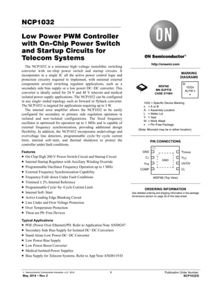
  • 1. © Semiconductor Components Industries, LLC, 2014 May, 2014 − Rev. 2 1 Publication Order Number: NCP1032/D NCP1032 Low Power PWM Controller with On-Chip Power Switch and Startup Circuits for Telecom Systems The NCP1032 is a miniature high−voltage monolithic switching converter with on−chip power switch and startup circuits. It incorporates in a single IC all the active power control logic and protection circuitry required to implement, with minimal external components several switching regulator applications, such as a secondary side bias supply or a low power DC−DC converter. This converter is ideally suited for 24 V and 48 V telecom and medical isolated power supply applications. The NCP1032 can be configured in any single−ended topology such as forward or flyback converter. The NCP1032 is targeted for applications requiring up to 3 W. The internal error amplifier allows the NCP1032 to be easily configured for secondary or primary side regulation operation in isolated and non−isolated configurations. The fixed frequency oscillator is optimized for operation up to 1 MHz and is capable of external frequency synchronization, providing additional design flexibility. In addition, the NCP1032 incorporates undervoltage and overvoltage line detectors, programmable cycle−by−cycle current limit, internal soft−start, and thermal shutdown to protect the controller under fault conditions. Features • On Chip High 200 V Power Switch Circuit and Startup Circuit • Internal Startup Regulator with Auxiliary Winding Override • Programmable Oscillator Frequency Operation up to 1 MHz • External Frequency Synchronization Capability • Frequency Fold−down Under Fault Conditions • Trimmed ± 2% Internal Reference • Programmable Cycle−by−Cycle Current Limit • Internal Soft−Start • Active Leading Edge Blanking Circuit • Line Under and Over Voltage Protection • Over Temperature Protection • These are Pb−Free Devices Typical Applications • POE (Power Over Ethernet)/PD. Refer to Application Note AND8247 • Secondary Side Bias Supply for Isolated DC−DC Converters • Stand Alone Low Power DC−DC Converter • Low Power Bias Supply • Low Power Boost Converter • Medical Isolated Power Supplies • Bias Supply for Telecom Systems. Refer to App Note AND8119/D http://onsemi.com MARKING DIAGRAMS 1032 = Specific Device Marking x = A or B A = Assembly Location L = Wafer Lot Y = Year W = Work Week G = Pb−Free Package PIN CONNECTIONS (Note: Microdot may be in either location) See detailed ordering and shipping information in the package dimensions section on page 20 of this data sheet. ORDERING INFORMATION WDFN8 MN SUFFIX CASE 511BH 1032x ALYW G G ÇÇ ÇÇ ÇÇ ÇÇ Ç Ç Ç Ç WDFN8 (Top View) GND GND CT VFB COMP VCC VDRAIN CL UV/OV 1
  • 2. NCP1032 http://onsemi.com 2 Figure 1. Typical Application – Dual Output Auxiliary Regulated Isolated Flyback D1 D2 COUT CVCC Cin R3 R4 RCL CCT CC RC CP R1 R2 NCP 1032 VDRAIN VCC CL COMP VFBGND CT UV/OV VIN VOUT 2.2 mF 22 mF 2.2 mF Figure 2. NCP1032 Simplified Block Diagram I1 3.0 V/ 3.5 V S R PWM COMP NCL NSS 30 ns One Shot − + 2.5 V Error Amplifier − + − + 5.7 V − + − + UV Comp OV Comp 2.24 V I2 Duty LEB ISET FB COMP OV/UV 7.6 V 10.2 V Fault Logic NUVLO NLOWVCC HIVCC NUVLO NLOWVCC HIVCC IN1 IN2 IN3 IN4 UVBAR UVBAR NUV OUT2 NUV NOV NOV IN5 IN6 nstart Fault Fault Fault LEBOUT LEBOUT Current Limit SS IN7Thermal Trip 12.5 mA PGND VDRAIN OUT3 Driver RT UVBAR Internal Bias nstart VCC Internal Bias Internal Bias (all pins except VDRAIN pin are protected by 10 V ESD diodes) Cycle = 75% Delay 2 kW 2 kW 1.0 V 2 kW 2 kW 2 kW 3.5 V 150 kW 2 kW 6.6 V Q SETCLR Q
  • 3. NCP1032 http://onsemi.com 3 Table 1. FUNCTIONAL PIN DESCRIPTION Pin Name Function Description 1 GND IC Ground Ground reference pin for the circuit. 2 CT Oscillator Frequency Selection An external capacitor connected to this pin sets the oscillator frequency up to 1 MHz. The oscillator can be synchronized to a higher frequency by charging or discharging CT to trip the internal 3.0 V/3.5 V comparators. If a fault condition exists, the power switch is disabled and the frequency is reduced. 3 VFB Feedback Signal Input The regulated voltage is scaled down to 2.5 V by means of a resistor divider. Regulation is achieved by comparing the scaled voltage to an internal 2.5 V reference. 4 COMP Error Amplifier Compensation The output of the internal error amplifier. External compensation network between COMP and VFB pin is required for stable operation. 5 CL Current Limit Threshold Selection A resistor RCL connected between this pin and ground sets the peak current value of the current limit. If the CL pin is left open, the current limit value is set to its initial maximum value of approximately 12 mA (CLIM_MAX). Programmable current limit threshold, together with internal soft−start feature effectively limits the primary transformer high current peaks during startup phase. 6 UV/OV Input Line Undervoltage and Overvoltage Shutdown Input line voltage is scaled down using an external resistor divider. The minimum operating Vin voltage is achieved when the voltage on UV/OV pin reaches UV threshold 1.0 V. The maximum operating voltage is then limited by 2.4 V on UV/OV pin. A device version without OV protection feature is available, see ordering information section. 7 VCC Powers the Internal Circuitry Supplies power to the internal control circuitry. Connect an external capacitor for energy storage during startup. The Vcc voltage should not exceed 16 V during operation. 8 VDRAIN Drain Connection Connects the power switch and startup circuit to the primary transformer windings. EP EP Thermal Flag This is the thermal flag for the IC and should be soldered to the ground plane. Table 2. MAXIMUM RATINGS Rating Symbol Value Unit Power Switch and Startup Circuits Voltage BVdss −0.3 to +200 V VCC Power Supply Voltage VCC −0.3 to +16 V Power Supply Voltage on all Pins, except VDRAIN and VCC VIO −0.3 to +10 V Drain Current Peak During Transformer Saturation IDS(pk) 1.0 A Thermal Resistance Junction−to−Air –W DFN8 3x3, case 511BH (100 sq mm, 2oz) (Note 4) (500 sq mm, 2oz) (Note 4) (100 sq mm,2oz,) (Note 5) RqJA 109 64 44 °C/W Maximum Junction Temperature TJMAX 150 °C Storage Temperature Range TSTG −60 to +150 °C ESD Capability, Human Body Model Pins 1−7 (Note 1) 4.0 kV ESD Capability, Machine Model Pins 1−7 (Note 1) 400 V Pin 8 is connected to the high voltage startup and power switch which is protected to the maximum drain voltage 200 V Stresses exceeding those listed in the Maximum Ratings table may damage the device. If any of these limits are exceeded, device functionality should not be assumed, damage may occur and reliability may be affected. 1. This device series contains ESD protection and passes the following tests: Human Body Model (HBM) ± 2.0 kV per JEDEC standard: JESD22−A114. Machine Model (MM) ± 200 V per JEDEC standard: JESD22−A115. 2. This device contains latch−up protection and it exceeds ± 100 mA per JEDEC standard: JESD78 class II 3. Moisture Sensitivity Level (MSL): 1 per IPC/JEDEC standard: J−STD−020A 4. EIA JEDEC 51.3, single layer PCB with added heat spreader 5. EIA JEDEC 51.7, four layer PCB with added heat spreader
  • 4. NCP1032 http://onsemi.com 4 Table 3. ELECTRICAL CHARACTERISTICS (For typical values Tj = 25°C, for min/max values Tj = −40°C to +125°C, VDRAIN = 48 V, VCC = 12 V, unless otherwise noted) Symbol Parameter Conditions Min Typ Max Unit SUPPLY SECTION AND VCC MANAGEMENT VCC_ON Vcc Voltage at Which the Switcher Starts Operation VCC Increasing 9.9 10.2 10.5 V VCC_MIN Minimum Operating VCC After Turn on at Which HV Current Source Restarts VCC Decreasing 7.40 7.55 7.7 V VCC_RST Vcc Undervoltage Lockout Voltage VCC Decreasing, VFB = VCOMP 6.75 6.95 7.15 V ICC1 Internal IC Consumption Power Switch Enabled MOSFET is switching at 300 kHz 2.0 2.9 4.0 mA ICC2 Internal IC Consumption Power Switch Disabled No Fault condition, VFB = 2.7 V − 2.0 2.5 mA ICC3 Internal IC Consumption Power Switch Disabled Fault condition, VFB = 2.7 V, VUV/OV < 1.0 V − 0.75 1.5 mA POWER SWITCH CIRCUIT RDSON Power Switch Circuit On−State Resistance ID = 100 mA TJ = 25°C TJ = 125°C − − 4.2 4.9 5.1 8.0 W BVdss Power Switch Circuit and Startup Breakdown Voltage IDS_OFF = 100 mA, VUV_OV < 1.0 V Tj = 25°C 200 − − V IDS_OFF Power Switch Circuit and Startup Circuit Off−State Leakage Current VDRAIN = 200 V, VUV_OV < 1.0 V TJ = 25°C TJ = −40°C to 125°C − − 20 20 25 30 mA tR Switching Characteristics − Rise Time VDS = 48 V, RL = 480 W, Time (10%−90%) − 7 − ns tf Switching Characteristics − Fall Time VDS = 48 V, RL = 480 W, Time (90%−10%) − 10 − ns INTERNAL STARTUP CURRENT SOURCE ISTART1 HV Current Source Vcc = 0 V, Tj = 25°C Tj = −40°C to 125°C 10.0 9.0 12.0 − 14.0 15.0 mA ISTART2 HV Current Source Vcc = VCC_ON − 0.2 V Tj = 25°C Tj = −40°C to 125°C 9.0 8.0 11.0 − 13.0 16.0 mA Vstart_min Minimum Startup Voltage ISTART2 = 0.5 mA, Vcc = VCC_ON − 0.2 V, Tj = 25°C − 16.3 − V ERROR AMPLIFIER VREF Reference Voltage VCOMP = VFB, Follower Mode TJ = 25°C TJ = −40°C to 125°C 2.45 2.40 2.5 2.5 2.55 2.60 V REGLINE Line Regulation VCC = 8 V to 16 V, TJ = 25°C − 1.0 3.0 mV IVFB Input Bias Current VFB = 2.3 V − 70 150 nA ISRC COMP Source Current VFB = 2.3 V 80 95 125 mA ISNK COMP Sink Current VFB = 2.7 V 500 700 900 mA VC_MAX COMP Maximum Voltage ISRC = 0 mA, VFB = 2.3 V 3.95 4.17 4.5 V VC_MIN COMP Minimum Voltage ISNK = 0 mA, VFB = 2.7 V − 91 200 mV AVOL Open Loop Voltage Gain (Note 6) − 80 − dB GBW Gain Bandwidth Product (Note 6) − 1.0 − MHz
  • 5. NCP1032 http://onsemi.com 5 Table 3. ELECTRICAL CHARACTERISTICS (For typical values Tj = 25°C, for min/max values Tj = −40°C to +125°C, VDRAIN = 48 V, VCC = 12 V, unless otherwise noted) Symbol UnitMaxTypMinConditionsParameter CURRENT LIMIT AND PWM COMPARATOR CLIM_MAX Max Current Limit Threshold CL pin Floating, TJ = 25°C, (di/dt = 0.5 A/ms) 420 512 600 mA CLIM_MIN Min Current Limit Threshold RCL = 20 kW, TJ = 25°C, (di/dt = 0.1 A/ms) − 57 − mA TPLH Propagation Delay from Current Limit Detection to the Drain OFF State (Note 6) − 100 − ns TON_MIN Min On Time Pulse Width FSW = 300 kHz (Note 6) − 240 − ns Tss Soft−Start Duration (Note 6) − 2.0 − ms LINE UNDER/OVERVOLTAGE PROTECTIONS Vuv Undervoltage Lockout Threshold VFB = VCOMP, Vin decreasing 0.95 1.067 1.18 V VUV_hys Undervoltage Lockout Hysteresis − 70 − mV Iuv Input Bias Current VFB = 2.3 V − 0 1 mA VOV Overvoltage Lockout Threshold VFB = VCOMP, Vin increasing (Note 7) 2.3 2.41 2.5 V Vov_hys Overvoltage Lockout Hysteresis − 158 − mV TEMPERATURE MANAGEMENT TSD Thermal Shutdown (Note 6) 175 °C Hysteresis in Shutdown (Note 6) 20 °C INTERNAL OSCILLATOR fOSC1 Oscillation Frequency, 300 kHz CT = 560 pF (Note 9) TJ = 25°C TJ = −40°C to 125°C 275 270 300 − 325 335 kHz fOSC2 Oscillation Frequency, 960 kHz CT = 100 pF, TJ = 25°C − 960 − kHz ICT_C Timing Charge Current VCT = 3.25 V − 172 − mA ICT_D Timing Discharge Current VCT = 3.25 V 517 mA VR_pk Oscillator Ramp Peak Voltage − 3.492 − V VR_VLY Oscillator Ramp Valley − 2.992 − V DCMAx Maximum Duty Cycle 70 76.5 80 % Product parametric performance is indicated in the Electrical Characteristics for the listed test conditions, unless otherwise noted. Product performance may not be indicated by the Electrical Characteristics if operated under different conditions. 6. Guaranteed by design and characterized 7. The OV/UV option is disabled on the NCP1032B version 8. Oscillator frequency can be externally synchronized to the maximum frequency of the device
  • 6. NCP1032 http://onsemi.com 6 TYPICAL OPERATING CHARACTERISTICS – Dual Output Isolated Flyback Converter Figure 3. Efficiency vs. IOUT at VIN = 24, 36, 48 and 72 V, T1 = CoilCraft B0226−EL Figure 4. VCC Pin Load Regulation at VIN = 24, 36, 48 and 72 V IOUT (mA) IOUT (mA) 2001751501007550250 0 10 20 30 50 60 70 80 2001751501007550250 12.060 12.065 12.070 12.075 12.080 12.090 12.095 12.100 Figure 5. Startup Sequence, RCL Open, Output Load = 80 W (IOUT = 150 mA), 1 VCC 3.0 V/ div DC, 2 VOUT 3.0 V/div DC, 3 VIN 10.0 V/ div DC, 4 IPRI 100 mA/div DC, T = 20 ms/div Figure 6. Soft−Start, RCL open, Output No Load 1 VCC 3.0 V/div DC, 2 VOUT 3.0 V/div DC, 3 VIN 10.0 V/div DC, 4 IPRI 100 mA/div DC, T = 500 ms/div Figure 7. Soft−Start, RCL = 32 kW (CLIM = 250 mA), Output Load = 240 W (IOUT = 50 mA), 1 VCC 3.0 V/div DC, 2 VOUT 3.0 V/div DC, 3 VIN 10.0 V/div DC, 4 IPRI 100 mA/div DC, T = 1.0 ms/div Figure 8. Discontinuous Conduction Mode (DCM), IOUT = 150 mA, 2 VDRAIN 20 V/div DC, 3 ISEC 30 mA/div DC, 4 IPRI 100 mA/div, DC, T = 500 ns/div EFFICIENCY(%) VOUT(V) 125 225 40 36 V 48 V 72 V 24 V 18 V 125 225 12.085 36 V 48 V 72 V 24 V 18 V
  • 7. NCP1032 http://onsemi.com 7 TYPICAL OPERATING CHARACTERISTICS Figure 9. Frequency vs. Timing Capacitor CT at 255C Figure 10. Oscillator Frequency vs. Junction Temperature CAPACITANCE (pF) AMBIENT TEMPERATURE (°C) 248020001520104056080 50 100 200 400 800 1600 100806040200−20−40 300 400 500 600 800 900 1000 1100 Figure 11. Maximum Duty Ratio vs. Temperature Figure 12. Maximum Duty Ratio vs. VCC Voltage AMBIENT TEMPERATURE (°C) VCC (V) 100806040200−20−40 74.0 74.2 74.6 74.8 75.0 75.4 75.8 76.0 15141312111098 74.0 74.3 74.6 74.9 75.2 75.5 Figure 13. Minimum On Time vs. VCC Figure 14. Power Switch Circuit and Startup Circuit Leakage Current vs. Drain Voltage VCC (V) DRAIN VOLTAGE (V) 15141312111098 100 120 160 180 220 240 280 300 24020016012080400 0 4 8 12 16 20 28 30 FREQUENCY(kHz) SWITCHINGFREQUENCY(kHz) DUTYCYCLE(%) DUTYCYCLE(%) MINONTIME(ns) IDS(off),POWERSWITCHANDSTARTUP CIRCUITSLEAKAGECURRENT(mA) 120 700 CT = 82 pF CT = 220 pF CT = 560 pF 120 74.4 75.2 75.6 1.04 MHz 597 kHz320 kHz 128 kHz 16 VDRAIN = 100 V VDRAIN = 48 V VDRAIN = 15 V 16 140 200 260 VDRAIN = 100 V VDRAIN = 48 V VDRAIN = 15 V 24 6 10 14 18 22 26 2 125°C 25°C −40°C
  • 8. NCP1032 http://onsemi.com 8 TYPICAL OPERATING CHARACTERISTICS Figure 15. Power Switch RDSON vs. Junction Temperature Figure 16. Vdrain Startup Threshold over Temperature TJ, JUNCTION TEMPERATURE (°C) TJ, JUNCTION TEMPERATURE (°C) 100806040200−20−40 2.9 3.1 3.5 3.9 4.3 4.7 5.1 5.5 100806040200−20−40 16.10 16.14 16.18 16.22 Figure 17. Startup Current vs. Junction Temperature Figure 18. Undervoltage Lockout Threshold vs. Junction Temperature TJ, JUNCTION TEMPERATURE (°C) TJ, JUNCTION TEMPERATURE (°C) 100806040200−20−40 10.2 10.4 10.8 11.2 11.6 11.8 12.4 12.8 100806040200−20−40 6.930 6.935 6.940 6.945 6.950 6.955 6.960 6.965 Figure 19. Supply Voltage Thresholds vs. Junction Temperature Figure 20. VCC Input Current at 12 V with an 18 V applied Drain voltage 255C VS Oscillator Frequency TJ, JUNCTION TEMPERATURE (°C) FREQUENCY (kHz) 100806040200−20−40 7.25 7.50 8.00 8.50 9.00 9.50 10.00 10.50 800700600500400300200100 2.00 2.25 3.00 3.25 3.75 4.25 4.75 5.25 RDS(on),POWERSWITCHON RESISTANCE(W) VCC(reset),UNDERVOLTAGE LOCKOUTTHRESHOLD(V) ISTART,STARTUPCURRENT(mA) VCC(reset),UNDERVOLTAGE LOCKOUTTHRESHOLD(V) UVTHRESHOLD(V) INPUTCURRENT(mA) 120 3.3 3.7 4.1 4.5 4.9 5.3 VCC = 16 V VCC = 12 V VCC = 8 V 16.12 16.16 16.20 16.24 16.30 16.34 16.38 16.28 16.32 16.36 16.40 16.26 120 120 10.6 11.0 11.4 12.0 12.2 12.6 VCC = VCC(on) − 0.2 V VCC = 0 V 120 120 7.75 8.25 8.75 9.25 9.75 10.25 Startup Threshold Minimum Operating Threshold 900 1000 2.50 2.75 3.50 4.00 4.50 5.00
  • 9. NCP1032 http://onsemi.com 9 TYPICAL OPERATING CHARACTERISTICS Figure 21. Operating Supply Current vs. Supply Voltage at 320 kHz Figure 22. VCC Input Current vs. Temperature over Frequency span VDrain = 48 V VCC, SUPPLY VOLTAGE (V) AMBIENT TEMPERATURE (°C) 15141312111098 2.1 2.3 2.7 2.9 3.1 3.5 3.7 4.1 100806040200−20−40 2.0 2.5 3.5 4.0 4.5 5.5 6.0 6.5 Figure 23. COMP Clamp Voltage vs. Junction Temperature Figure 24. Reference Voltage vs. Junction Temperature TJ, JUNCTION TEMPERATURE (°C) TJ, JUNCTION TEMPERATURE (°C) 100806040200−20−40 4.11 4.12 4.14 4.16 4.18 4.20 4.21 4.23 100806040200−20−40 2.488 2.490 2.491 2.493 2.495 2.496 2.498 2.500 Figure 25. COMP Source Current vs. Junction Temperature Figure 26. COMP Sink Current vs. Junction Temperature TJ, JUNCTION TEMPERATURE (°C) TJ, JUNCTION TEMPERATURE (°C) 100806040200−20−40 94.00 94.25 94.75 95.00 95.25 95.75 96.00 96.50 100806040200−20−40 620 640 680 700 720 740 780 800 ICC1,OPERATINGSUPPLY CURRENT(mA) INPUTCURRENT(mA) VcCLAMP(V) REFERENCEVOLTAGE(V) SOURCECURRENT(mA) SINKCURRENT(mA) 16 2.5 3.3 3.9 VDRAIN = 48 V TJ = 25°C CT = 560 pF 120 3.0 5.0 1.04 MHz 597 kHz 320 kHz 128 kHz 2.489 2.492 2.494 2.497 2.499 120 VCC = 16 V VCC = 12 VVCC = 8 V 120 94.50 95.50 96.25 VCC = 16 V VCC = 12 V VCC = 8 V 120 660 760 120 4.13 4.15 4.17 4.19 4.22
  • 10. NCP1032 http://onsemi.com 10 TYPICAL OPERATING CHARACTERISTICS Figure 27. Undervoltage Threshold vs. Junction Temperature Figure 28. Overvoltage Threshold vs. Junction Temperature TJ, JUNCTION TEMPERATURE (°C) TJ, JUNCTION TEMPERATURE (°C) 100806040200−20−40 1.060 1.061 1.063 1.065 1.067 1.069 1.070 1.072 100806040200−20−40 2.394 Figure 29. Under/Overvoltage Hysteresis vs. Junction Temperature Figure 30. Current Limit Threshold vs. RCL, Current Slew Rate = 0.5 A/ms TJ, JUNCTION TEMPERATURE (°C) RISET (kW) 100806040200−20−40 60 80 90 110 130 150 160 180 18014012010080604020 50 100 150 200 250 350 400 450 Figure 31. Current Limit Threshold vs. Current Slew Rate Figure 32. Current Limit Threshold vs. TJ, Current Slew RISET = Open = 0.5 A/ms, RISET = 55 kW = 0.3 A/ms, RISET = 22 kW = 0.1 A/ms CURRENT SLEW RATE (mA/mS) TJ, JUNCTION TEMPERATURE (°C) 10008007004003002001000 270 280 290 300 310 320 330 340 100806040200−20−40 50 100 200 250 300 400 500 550 UVTHRESHOLD(V) OVTHRESHOLD(V) VUV/OV(hys),HYSTERESIS(mV) ILIM,CURRENTLIMITTHRESHOLD(mA) ILIM,CURRENTLIMITTHRESHOLD(mA) VCC = 16 V VCC = 12 V VCC = 8 V 120 1.062 1.064 1.066 1.068 1.071 VCC = 16 V VCC = 12 V VCC = 8 V 120 2.396 2.398 2.400 2.402 2.404 2.406 2.408 2.410 2.412 2.414 2.416 2.418 2.420 2.422 70 100 120 140 170 120 OV Hysteresis UV Hysteresis 160 200 300 600500 900 25 V 72 V 120 mH ILIM,CURRENTLIMITTHRESHOLD(mA) 120 150 350 450 RISET = OPEN RISET = 50 kW RISET = 22 kW
  • 11. NCP1032 http://onsemi.com 11 CT Ramp CT Charge Signal PWM Comparator Output Power Switch Circuit Gate Drive PWM Latch Output Leading Edge Blanking Output Current Limit Propagation Current Limit Threshold Output OverloadNormal PWM Operating Range Figure 33. Pulse Width Modulation Timing Diagram Delay Output OverloadNormal OperationStartup Mode Dynamic Self Supply VCC(on) VCC(off) VCC(reset) 0 V ISTART 0 mA 0 V 3.0 V 2.5 V 0 V 0 V Figure 34. Auxiliary Winding Operation with Output Overload Timing Diagram VDRAIN VFB VUV
  • 12. NCP1032 http://onsemi.com 12 Introduction The NCP1032 is a monolithic voltage−mode switching regulator designed for isolated and non−isolated bias supply applications. The internal startup circuit and the MOSFET are rated at 200 V, making them ideal for 24 V through 48 V telecom and 42 V automotive applications. In addition, the NCP1032 can operate from an existing 12 V supply. The regulator is optimized for operation up to 1 MHz. The NCP1032 device incorporates all of the active power, control logic, protection circuitry, and power switch in a single IC. The compact design allows the designer to use minimal external components on several switching regulator applications, such as a secondary side bias supply or a low power DC−DC converter. The NCP1032 is available in the space saving WDFN8 3 x 3 mm package and is targeted for applications requiring up to 3 W. The NCP1032 has an extensive set of features including programmable cycle−by−cycle current limit, internal soft−start, input line under and over voltage detection comparators with hysteresis, regulator output undervoltage lockout with hysteresis and over temperature protection providing protection during fault conditions. A description of each of the functional blocks is given below and the functional block diagram is shown in Figure 2. Startup Supply Circuit and Undervoltage Lockout The NCP1032 contains an internal 200 V startup regulator that eliminates the need for external startup components. The startup regulator consists of a 12 mA (typical) current source that supplies power from the input line (VDRAIN) pin to charge the capacitor on the VCC pin (CVCC). The act of charging the CVCC capacitor until it reaches 10.2 V while holding the power switch off is called Startup Mode (SM). Once the current source charges the VCC voltage to 10.2 V (typical) the startup circuit is disabled and if no faults are present, the power switch circuit is enabled. The internal control circuitry will draw its current from the energy held by the CVCC capacitor. The startup regulator turns on again once VCC reaches 7.55 V. The charging of the CVCC capacitor to 10.2 V by the current source and the discharging by the control circuitry to 7.55 V will be henceforth referred to as Dynamic Self Supply (DSS). If VCC falls below 7.55 V while switching, the device enters a Restart Mode (RM). While in the RM the CVCC capacitor is allowed to discharge to 6.95 V while the power switch is enabled. Once the 6.95 V threshold is reached, the power switch circuit is disabled, and the startup regulator is enabled to charge the CVCC capacitor. The power switch is enabled again once the VCC voltage reaches 10.2 V. Therefore, the external CVCC capacitor must be sized such that a voltage greater than 6.95 V is maintained on the VCC pin while the converter output reaches regulation. The output is delayed 0.4 ms (TSS_Delay) from the released undervoltage lockout to the first switching pulse. The soft−start time TSS is fixed at 2 ms to ramp the current from its minimum value to its maximum value. The soft−start time is load and RCL dependent and can be computed in the soft−start section. The designer must evaluate the current draw of the regulator at the desired switching frequency over the VCC and temperature operating range shown in Figures 20 − 22. CVCC is calculated using the following equation: CVCC + ICC ǒTSS_Delay ) TSS Ǔ VCC_ON * VCC_MIN ³ 2.95 mF + 4.0 mA ǒ0.4 ms ) 2.0 msǓ 10.2 V * 6.95 V (eq. 1) ICC includes the NCP1032 bias current (ICC1_MAX) and any additional current used to bias the feedback (if used). Assuming an ICC1_MAX of 3.5 mA plus a 0.5 mA bias current for the feedback sensing resistors (if used), and Tss of 2 ms, CVCC is calculated at 2.95 mF and should be rounded up to ensure design margin to 3.3 mF. Please note that if the feedback sensing resistors are connected to the VCC pin (isolated main output topology) and CVCC is increased to match COUT, the transient response of the converter will suffer. The poor transient response is due to the imbalanced capacitance to current ratio. The auxiliary winding has a significantly greater capacitance to current ratio than the output winding, taking it longer for CVCC to follow COUT during a transient condition. After initial startup, the VCC pin should be biased above VCC_min using an auxiliary winding. This will prevent the startup regulator from turning on during normal operation, reducing device power dissipation. A load should not be directly connected to the VCC pin. A load greater than 12 mA will override the startup circuit possibly damaging the part. The maximum voltage rating of the startup circuit is 200 V. Power dissipation should be observed to avoid exceeding the maximum power dissipation of the package. Figure 35 shows the recommended configuration for a non−isolated flyback converter. Figure 35. Non−Isolated Bias Supply Configuration D1 D2 COUT CVCC Cin R3 R4 RCL CCT CC RC CP R1 R2 VDRAIN VCC CL COMP VFB GND CT UV/OV VIN VOUTT1 Lsec Lbias Lpri NCP1032
  • 13. NCP1032 http://onsemi.com 13 Soft−Start The NCP1032 features an internal soft−start which reduces power−on stress and also contributes to the lower output overshoot. Once the VCC_ON threshold is reached and there are no fault conditions, the power switch is enabled and the cycle−by−cycle current limit is ramped up slowly to the current limit threshold set by the CL pin. If the CL pin is open, the current limit will be set to its maximum value and the soft−start time will be 2 ms as shown in Figure 36. The equation below can be used to calculate the soft−start time for all other current limit set values. TSSR + SetCurrent * MinCurrent MaxCurrent * MinCurrent TSS ³ 1.07 ms + 300 mA * 57 mA 512 mA * 57 mA 2 ms (eq. 2) COMP Voltage 4.2 V 3.5 3.0 V PWM Signal Ramp Inductor Current Current Limit 57 mA Set Limit Soft−Start Time Correction Time Figure 36. Soft−Start Time The compensation of the converter must be manipulated to minimize the overshoot of the output voltage during startup, details are in the compensation section. Line Under and Over Voltage Detectors The NCP1032 incorporates Vin input line under voltage (UV) and over voltage (OV) shutdown circuits. If the UV/OV pin is set below 1.0 V or above 2.4 V thresholds the power switch will stop switching and the part will use DSS until the problem is corrected. The comparators incorporate typical voltage hysteresis of 70 mV (UV) and 158 mV (OV) to prevent noise from inadvertently triggering the shutdown circuit. The UV/OV sense pin can be biased using an external resistor divider from the input line as shown in Figure 37. The UV/OV pin should be bypassed using a 1 nF capacitor to prevent triggering the UV/OV circuit during normal switching operation. R3 VIN 1 nF R4 1 V 2.4 V OV Comparator UV Comparator Fault OV Enable Figure 37. UV/OV Resistor Divider from the Input Line CUV Logic The resistive network impedance must not be too high to keep good voltage accuracy and not too low to minimize power losses. A 200 kW to 1.2 MW range is recommended for the high side resistor R3. If the designer wanted to set the undervoltage threshold to 32 V, the resistor divider should be designed according to the following equation: R4 + VUV R3 VIN_UV * VUV ³ 34.49 kW + 1.067 1 MW 32 V * 1.067 [ 34.0 kW (R96 Value) (eq. 3)
  • 14. NCP1032 http://onsemi.com 14 The OV threshold monitored at the UV/OV pin is 2.41 times higher than the UV threshold, leading to an OV threshold of 73.3 V for the calculated R96 value. Designers can quickly set the OV/UV thresholds by referencing Figure 38. Figure 38. UV/OV Resistor Divider Thresholds with R4 Set to 10 k R3 (kW) 450400 500350300250200150 10 20 40 50 70 90 100 120 INPUTVOLTAGE(V) 30 60 80 110 Overvoltage Threshold Undervoltage Threshold The UV/OV pin can also be used to implement a remote enable/disable function. If an external transistor pulls the UV/OV pin below 1.0 V (or above 2.4 V) the converter will be disabled and no switching is allowed. A device version is available without the OV protection feature, see the ordering information section. Error Amplifier The internal error amplifier (EA) regulates the output voltage of the bias supply. The scaled signal is fed into the feedback pin (VFB) which is the inverting input of the error amplifier. It compares a scaled voltage signal to an internal trimmed 2.5 V reference connected to its non−inverting input. The output of the error amplifier is internally connected to a PWM comparator and also available externally through the COMP pin for frequency compensation. To insure normal operation, the EA compensation should be selected such that the EA frequency response crosses 0 dB below 80 kHz. The error amplifier feedback bias current is less than 200 nA over the operating range. The output source and sink currents are typically 95 mA and 700 mA, respectively. Under load transient conditions, COMP may need to move from the bottom to the top of the CT ramp. A large current is required to complete the COMP swing if small resistors or large capacitors are used to implement the compensation network. In which case, the COMP swing will be limited by the EA source current. Optimum transient responses are obtained if the compensation components allow the COMP pin to swing across its operating range in 1 cycle. Oscillator, Voltage Feed Forward, and Sync Capability The oscillator is optimized for operation up to 1 MHz and its frequency is set by the external timing capacitor (CT) connected to the CT pin. The oscillator has two modes of operation: free running and synchronized (sync). While in free running mode, an internal current source sequentially charges and discharges CT generating a voltage ramp between 3.0 V and 3.5 V. Under normal operating conditions, the charge (ICT_C) and discharge (ICT_D) currents are typically 172 mA and 515 mA, respectively. The charge/discharge current ratio of 1:3 discharges CT in 25% of the total period. The power switch is disabled while CT is discharging, guaranteeing a maximum duty cycle of 75% as shown in Figure 39. 25% 75%Signal Power Switch Enabled COMP Max Duty Cycle Figure 39. Auxiliary Winding Operation with Output Overload Timing Diagram CT Ramp CT Charge The oscillator frequency should be set no more than 25% below the target sync frequency to maintain an adequate voltage ramp and provide good noise immunity. A possible circuit to synchronize the oscillator is shown in Figure 40. C1 R1 R2 2 Figure 40. External Frequency Synchronization Circuit CT CT
  • 15. NCP1032 http://onsemi.com 15 Voltage feed forward can be implemented by connecting a resistor from the input voltage to the CT pin. RFF supplies a current that allows the input voltage to modify the maximum duty cycle rather than the standard 75% maximum. If the designer wanted to implement a fixed lower duty cycle, a resistor can be tied to a fixed voltage source such as VAUX or a voltage reference. If voltage feed forward is used, the frequency can shift dramatically depending on the value of the resistor. Cin RFF CCT NCP1032 VDRAIN GND CTVIN Z1 4 V IFF 2.2 mF Off On Time Off Time On Time 66% Off On Time 75% 58% 53% Off Time On Time 42% Off Time On Time 38% Off Time On Time 29% Off Time On 21% Off Time On Feed Forward Voltage CT PIN Voltage Figure 41. Voltage Feed Forward RVFF + VINMIN * Ramp ICT_D * DMAX ǒICT_C ) ICT_D Ǔ ³ 320 kW + 32 V * 3.25 V 517 mA * 62% ǒ172 mA ) 517 mAǓ (eq. 4) PWM Comparator and Latch The Pulse Width Modulator (PWM) comparator compares the error amplifier output (COMP) to the CT ramp and generates a proportional duty cycle. The power switch is disabled while COMP voltage is below the CT ramp signal. Once COMP reaches the ramp signal, the power switch is enabled. If COMP is at the bottom of the CT ramp, the converter operates at minimum duty cycle. While COMP increases, the duty cycle increases until COMP reaches the peak of the CT ramp, at which point the controller operates at maximum duty cycle. The CT charge signal is filtered through a one shot pulse generator to set the PWM latch and enable switching at the beginning of each period. Switching is allowed while the CT ramp is below COMP and a current limit fault is not present. The pulse width modulation technique is seen in Figure 39. The PWM comparator and latch propagation delay are less than 200 ns. If the system is designed to operate with a minimum on time less than 200 ns (no or light load), the converter will skip pulses. Skipping pulses is usually not a problem, unless operating at a frequency close to the audible range. Skipping pulses is more likely when operating at high frequencies during high input voltage and minimum load conditions. A 2 kW series resistor is included for ESD protection between the internal EA output and the COMP pin. Under normal operation, a 220 mV offset is observed between the CT ramp and the COMP crossing points. The series resistor does not interact with the error amplifier transfer function. Programmable Current Limit The power switch circuit incorporates SENSEFET® technology to monitor the drain current. A sense voltage is generated bydrivinga sense element, RSENSE, with a current proportional to the drain current. The sense voltage is compared to an externally programmable reference voltage on the non−inverting input of the current limit comparator. If the sense voltage exceeds the setup reference level, the comparator resets the PWM latch and the switching cycle is terminated. The reference level threshold is programmable by a resistor (RCL) connected to the CL pin shown in Figure 42. By limiting the peak current to the needs of the application, the transformer sizing can be scaled appropriately to the specific requirements which allows the PCB footprint to be minimized. The NCP1032 maximum drain current limit thresholds are 512 mA. RCL + 114 ln(Rset) * 142 (eq. 5) RCL + 309 ln(Rset) * 893 Rset t 42.2 kW 200 kW u Rset u 42.2 kW Current Limit Comparator Fault Logic Sense MOSFET DRIVER Leading Edge Blanking GND VDRAIN 100 ns RCL Soft−Start Ramp+ + − CL Figure 42. Current Limit Threshold and Propagation Delay 3.2 mA
  • 16. NCP1032 http://onsemi.com 16 The propagation delay is measured from the time an overcurrent fault appears at power switch circuit drain, to the start of the turn−off transition as shown in Figure 43. The current limit propagation delay time is typ. 100 ns. The propagation must be accounted for when designing the power supply, as it will result in a constant power output through the transformer when the output is shorted. The constant power can cause the transformer to rise in temperature permanently damaging the magnetics. This can be mitigated by placing a 10 W resistor in series with the output rectification diode. t Figure 43. Current Limit Threshold and Propagation Delay ISW ILIM TPHL VIN LP TPHL Adaptive Leading Edge Blanking Each time the power switch circuit is turned on, a narrow voltage spike appears across RSENSE. The spike is due to the power switch circuit gate to source capacitance, transformer interwinding capacitance, and output rectifier recovery time. The spike can cause a premature reset of the PWM latch. A proprietary active Leading Edge Blanking (LEB) circuit masks the current signal to prevent the voltage spike from resetting the PWM latch. The active LEB masks the current signal until the power switch turn on transition is complete. The adaptive LEB period provides better current limit control compared to a fixed blanking period. Power Switch Circuit Protection The NCP1032 monolithically integrates a 200 V power switch with control logic circuitry. The power switch is designed to directly drive the converter transformer. The gate drive is tailored to control switching transitions and help limit electromagnetic interference (EMI). For a Flyback topology a large transient voltage spike appears at the transformers primary side after the power switch turns off. These spikes are a function of the transformer leakage inductance (LLP) on either the primary or secondary side. A circuit is needed to clamp the leakage spike, limiting the voltage drain excursion to a safe value. The operating VDRAIN_MAX is 200 V as depicted in Figure 44. Two such circuits are the passive RCD network or a zener clamp as depicted in Figure 45 and Figure 46. t Figure 44. Power Switch Waveforms with Clamping VIN VCLAMP VR VDRAIN VLS (leakage spike) VDRAIN_MAX (180 V) Vin D_Clamp Cclamp − + Cin D1 + Rcl T1 − Cvcc Cout Rclamp U? NCP1032_33 VCC 7 VDRAIN 8 CL 5 VFB 3 COMP 4 GND 1 UV/OV 6 CT 2 Figure 45. Passive RCD Clamp Network VF The passive RCD network is the most standard circuitry and the formula below is used to calculate RCLAMP and CCLAMP. RCLAMP + 2 VCLAMP ǒVCLAMP * (VOUT ) VF) NǓ LLP IPEAK 2 FSW CCLAMP + VCLAMP VLS FSW RCLAMP (eq. 6)
  • 17. NCP1032 http://onsemi.com 17 The voltage leakage spike (VLS) is usually selected 50 to 70% above the reflected value VR = N x (VOUT + VF) and (VIN + VCLAMP) must be below the operating VDRAIN−MAX which is 200 V. The diode used for the clamping circuit needs to be at minimum fast or ultrafast recovery and an MURA110 represents a good choice. One major drawback of the RCD network lies in its dependency upon the peak current. The worse case occurs when IPEAK and VIN are at the maximum. Dz_clamp Vin D_Clamp − + Cin D1 + Rcl T1 − Cvcc Cout U? NCP1032_33 VCC 7 VDRAIN 8 CL 5 VFB 3 COMP 4 GND 1 UV/OV 6 CT 2 Figure 46. Zener Clamp Network VF The zener diode is probably the most expensive but offers the best protection and a very precise clamping level. Select the zener voltage to set VLS level between 10 to 15 V above the reflected voltage VR so VZener = VLS + VR. The zener diode must be able to handle the voltage rating and power dissipation during the switch turn−off time. For the NCP1032, a 0.5 W zener diode, like the MMSZ47T1 is suitable. Thermal Shutdown Internal thermal shutdown circuitry is provided to protect the integrated circuit in the event that the maximum junction temperature is exceeded. When activated at 165°C, the power switch circuit is disabled. Once the junction temperature falls below 145°C, the NCP1032 is allowed to resume normal operation. This feature is provided to prevent catastrophic failures from accidental device overheating. It is not intended to be used as a substitute for proper heat sinking. Application Considerations Typical Applications A 12 V / 3 W bias supply for 36 V to 75 V telecom systems, 1500 V isolation DC−DC converters. The NCP1032 is configured in Flyback topology and operates in Discontinuous Conduction Mode (DCM) to offer a low−cost, high efficiency solution. The circuit schematic is shown in Figure 47. Transformer T1 is available as a CoilCraft B0226−EL. Capacitor CCT sets the switching frequency at approximately 300 kHz. Output voltage regulation and overall efficiency are shown in Figure 3 and Figure 4 on page 6. The resistor divider formed by R3 and R4 sets the undervoltage lockout threshold at about 32 V. Application Note AND8119/D describes the design of this bias supply system. − + 2.2 mF Cin D2 NRVB0540 R2 5.1 K R1 19.6 K 2.2 mF Cvcc D1 MBR140 22 mF Cout + Cc 100 nF Rc 18 K Cp 68 pF R3 1 M R4 32.4 560 pF Cct T1 Lsec Lpri Lbias U1 NCP1032 VCC 7 VDRAIN 8 CL 5 VFB 3 COMP 4 GND 1 UV/OV 6 CT 2 L1 2.2mH Cclp 1 nF MBR1H100 Dclp Rclp 18 k 1000 pF C1 1 nF Cuv − Figure 47. 48 V to Isolated 12 V / 3 W Bias Supply Schematic
  • 18. NCP1032 http://onsemi.com 18 Layout Recommendations To prevent EMI problems high current copper traces which have high frequency switching should be optimized. Therefore, use short and wide traces for power current paths and for power ground traces especially transformer trace connections (primary and secondary). When power is transferred from input to output, there is a period of time when the power switch is on, referred to as “on time,” and a period of time when the switch is off, referred to as “off time.” When the power switch is on, the input voltage is applied across the primary side of the transformer and current increases in the primary inductance. Further, when the power switch is on the output current is supplied from the output capacitance. When the power switch is off, current on the primary side conducts through the clamp or snubber circuit. On the secondary side current is conducting through the rectification diode, providing power to the output and replenishing energy in the output capacitances as shown in Figure 48. Electromagnetic radiation is minimized by keeping VDRAIN leads, output diode, and output bypass capacitor leads as short as possible. It is important to minimize the area of the VDRAIN nodes and used the ground plane under the switcher circuitry to prevent interplane coupling and minimize cross−talk to sensitive signals and ICs. The exposed pad of the package must be connected to the ground plane of the board which is important for EMI and thermal management. Finally, it is always good practice to keep sensitive traces such as feedback connection (VFB and COMP) as far away from switched signal connections (VDRAIN) as possible. Figure 48 shows an example of an optimized PCB layout. Thermal Considerations Careful attention must be paid to the internal power dissipation of the NCP1032. Power dissipation is a function of efficiency and output power. As output power requirements increase, proper component selection includes adjusting RDSON, forward voltage of diodes, and enlarging packages. For example, if a transformer’s size were increased to lower the DCR or/and increase the inductance efficiency will improve at heavier loads. The exposed thermal pad is designed to be soldered to the ground plane used as a heat sink. The ground plane size should be maximized and connected to the internal and bottom copper ground planes with thermal vias placed directly under the package to spread heat generated by the NCP1032 as depicted Figure 48. Figure 48. Recommended PCB Layout
  • 19. NCP1032 http://onsemi.com 19 − + 2.2 mF Cin R2 20 K R1 20 K D1 MBR140SFT1G 22 mF Cout + Cc 100 nF Rc 18 K Cp 68 pF R3 1 M R4 32.4 560 pF Cct Vin 32 to 75 V LsecLpri U1 NCP1032 VCC 7 VDRAIN 8 CL 5 VFB 3 COMP 4 GND 1 UV/OV 6 CT 2 Cclp 1 nF MBR1H100SFT3G Dclp Rclp 18 k 1 nF Cuv − Vout 5.0 V 600 mA D4 MMSZ5243BT1G Q1 NSS1C201LT1G R7 18 k T14:1 1.0 mF Cvcc Figure 49. 48 V to 5.0 V DC−DC Converter Without Auxiliary Winding − + 2.2 mF Cin R2 20 K R1 20 K D1 MBR140SFT1G 22 mF Cout + Cc 100 nF Rc 18 K Cp 68 pF R3 1 M R4 32.4 560 pF Cct Lpri Vin 32 to 75 V Lsec U1 NCP1032 VCC 7 VDRAIN8 CL 5 VFB 3 COMP 4 GND 1 UV/OV 6 CT 2 Cclp 1 nF MBR1H100SFT3G Dclp Rclp 18 k 1 nF Cuv − Vout 12.0 V 300 mA T13:1 100 nF Cvcc Figure 50. 48 V to 12.0 V DC−DC Converter Without Auxiliary Winding
  • 20. NCP1032 http://onsemi.com 20 D1 MURA115 COUT 22 mF Cin 1 mF R3 294 kW RCL 40.2 kW CCT CC 1.5 nF CP 100 pF R1 78.7 kW NCP1032 VDRAIN VCC CL COMP VFB GND CT UV/OV VIN VOUT 560 mF 100 V 50 mA R4 10 kW R2 2 kW RC 100 kW Figure 51. Typical Application Circuit Boost Circuit Configuration ORDERING INFORMATION Device OV Protection Marking Package Shipping† NCP1032AMNTXG Enable 1032A WDFN8 3x3 (Pb−Free) 3,000 / Tape & Reel NCP1032BMNTXG Disable 1032B WDFN8 3x3 (Pb−Free) 3,000 / Tape & Reel †For information on tape and reel specifications, including part orientation and tape sizes, please refer to our Tape and Reel Packaging Specifications Brochure, BRD8011/D.
  • 21. NCP1032 http://onsemi.com 21 PACKAGE DIMENSIONS WDFN8 3x3, 0.65P CASE 511BH ISSUE O NOTES: 1. DIMENSIONING AND TOLERANCING PER ASME Y14.5M, 1994. 2. CONTROLLING DIMENSION: MILLIMETERS. 3. DIMENSION b APPLIES TO PLATED TERMINAL AND IS MEASURED BETWEEN 0.15 AND 0.30 MM FROM TERMINAL TIP. 4. COPLANARITY APPLIES TO THE EXPOSED PAD AS WELL AS THE TERMINALS. ÇÇÇÇ ÇÇÇÇÇÇÇÇ AD E B C0.10 PIN ONE 2X REFERENCE 2X TOP VIEW SIDE VIEW BOTTOM VIEW L D2 E2 C C0.10 C0.10 C0.08 A1 SEATING PLANE 8X NOTE 3 b8X 0.10 C 0.05 C A BB DIM MIN MAX MILLIMETERS A 0.70 0.80 A1 0.00 0.05 b 0.25 0.35 D 3.00 BSC D2 2.20 2.40 E 3.00 BSC E2 1.40 1.60 e 0.65 BSC L 0.20 0.40 1 4 8 *For additional information on our Pb−Free strategy and soldering details, please download the ON Semiconductor Soldering and Mounting Techniques Reference Manual, SOLDERRM/D. SOLDERING FOOTPRINT* 0.65 PITCH 1.66 3.30 1 DIMENSIONS: MILLIMETERS 0.53 8X NOTE 4 0.40 8X DETAIL A A3 0.20 REF A3 ADETAIL B L1 DETAIL A L ALTERNATE CONSTRUCTIONS ÉÉÉÇÇÇ A1 A3 L ÇÇÇÉÉÉ ÉÉÉDETAIL B MOLD CMPDEXPOSED Cu ALTERNATE CONSTRUCTIONS L1 −−− 0.15 OUTLINE PACKAGE e RECOMMENDED K 0.45 REF 5 2.46 ON Semiconductor and are registered trademarks of Semiconductor Components Industries, LLC (SCILLC). SCILLC owns the rights to a number of patents, trademarks, copyrights, trade secrets, and other intellectual property. A listing of SCILLC’s product/patent coverage may be accessed at www.onsemi.com/site/pdf/Patent−Marking.pdf. SCILLC reserves the right to make changes without further notice to any products herein. SCILLC makes no warranty, representation or guarantee regarding the suitability of its products for any particular purpose, nor does SCILLC assume any liability arising out of the application or use of any product or circuit, and specifically disclaims any and all liability, including without limitation special, consequential or incidental damages. “Typical” parameters which may be provided in SCILLC data sheets and/or specifications can and do vary in different applications and actual performance may vary over time. All operating parameters, including “Typicals” must be validated for each customer application by customer’s technical experts. SCILLC does not convey any license under its patent rights nor the rights of others. SCILLC products are not designed, intended, or authorized for use as components in systems intended for surgical implant into the body, or other applications intended to support or sustain life, or for any other application in which the failure of the SCILLC product could create a situation where personal injury or death may occur. Should Buyer purchase or use SCILLC products for any such unintended or unauthorized application, Buyer shall indemnify and hold SCILLC and its officers, employees, subsidiaries, affiliates, and distributors harmless against all claims, costs, damages, and expenses, and reasonable attorney fees arising out of, directly or indirectly, any claim of personal injury or death associated with such unintended or unauthorized use, even if such claim alleges that SCILLC was negligent regarding the design or manufacture of the part. SCILLC is an Equal Opportunity/Affirmative Action Employer. This literature is subject to all applicable copyright laws and is not for resale in any manner. PUBLICATION ORDERING INFORMATION N. American Technical Support: 800−282−9855 Toll Free USA/Canada Europe, Middle East and Africa Technical Support: Phone: 421 33 790 2910 Japan Customer Focus Center Phone: 81−3−5817−1050 NCP1032/D SENSEFET is a registered trademark of Semiconductor Components Industries, LLC. LITERATURE FULFILLMENT: Literature Distribution Center for ON Semiconductor P.O. Box 5163, Denver, Colorado 80217 USA Phone: 303−675−2175 or 800−344−3860 Toll Free USA/Canada Fax: 303−675−2176 or 800−344−3867 Toll Free USA/Canada Email: orderlit@onsemi.com ON Semiconductor Website: www.onsemi.com Order Literature: http://www.onsemi.com/orderlit For additional information, please contact your local Sales Representative