1. ICs for Audio Common Use
s Overview
The AN7171NK and AN7176K are ICs for power ampli-
fication of 14W (13.2V, 4Ω) output. It can provide stereo
operation since two BTL amplifiers are incorporated in a
chip. It incorporates various protective circuits, thus pro-
viding high reliability. The circuits can be turned on or off
with supply pins energized, because the stand-by circuit
is built-in.
s Features
• Two BTL 14W outputs built-in
• Stand-by circuit built-in
• Various protective circuits (for temperature, or against
over-voltage, short-circuit between output and earth
and between output and VCC, load short-circuit)
• Small shock noise at power ON/OFF
• Fewer external components required
• Good oscillation stability
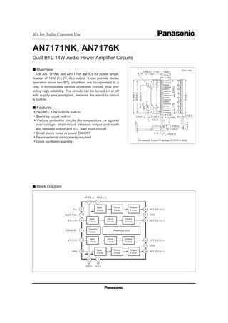
AN7171NK, AN7176K
Dual BTL 14W Audio Power Amplifier Circuits
Unit : mm
6.33±0.5
29.6±0.3
5.9±0.25 7.7±0.3 7.8±0.5
1
16
29.96±0.3
0.6±0.21.778
ø 3.6
28.0±0.3
20.0±0.25
R1.8
0.6
1.2±0.1
3.5±0.32.66
2.8±0.3 12.5±0.3
(14.1)
(4.06)
2.54±0.8
(0.25)
1.45±0.25
1.8±0.25
(1.2) 1.45±0.25
Fin-attached 16-lead ZIP package (EZIP016-P-0660)
s Block Diagram
1
13
6
5
12
10
11 9
14
15
16
4
3
2
8 7
VCC
Ripple Filter
(Ch.1) IN
STAND-BY
(Ch.2) IN
GND
OUT (Ch.1) (+)
GND
OUT (Ch.1) (–)
OUT (Ch.2) (+)
OUT (Ch.2) (–)
GND
Input
Circuit
Driver
Circuit
Output
Circuit
Input
Circuit
Driver
Circuit
Output
Circuit
Input
Circuit
Driver
Circuit
Output
Circuit
Input
Circuit
Driver
Circuit
Output
Circuit
Stand-by
Circuit
Protection Circuit
NF
(Ch.2)
NF
(Ch.2)
NF (Ch.1) NF (Ch.1)
2. ICs for Audio Common Use AN7171NK, AN7176K
Pin No. Pin Name
1
2
3
4
5
6
7
8
VCC
Output Ch.1 (+)
GND (Output Ch.1)
Output Ch.1 (–)
Stand-by
Input Ch.1
Negative Feedback Ch.1
Negative Feedback Ch.1
Pin No. Pin Name
9
10
11
12
13
14
15
16
Negative Feedback Ch.2
GND (Input)
Negative Feedback Ch.2
Input Ch.2
Ripple Filter
Output Ch.2 (–)
GND (Output Ch.2)
Output Ch.2 (+)
s Pin Descriptions
s Absolute Maximum Ratings (Ta= 25˚C)
VCC
Note 1)
VCC (surge)
Note 2)
ICC
PD
Note 3)
Topr
Tstg
Supply Voltage
Peak Supply Voltage
Supply Current
Power Dissipation
Operating Ambient Temperature
Storage Temperature
V
V
A
W
˚C
˚C
Parameter Symbol Rating Unit
24
50.0
6.0
37.5 Note 4)
– 30 ~ + 75
– 55 ~ + 150
Note 1) When no signals
Note 2) Time = 0.2s
Note 3) Rθj – c = 2˚C/W
Note 4) Ta = 75˚C
s Electrical Characteristics (VCC = 13.2V, RL= 4Ω, f = 1kHz, Ta = 25˚C)
Parameter Symbol Condition min. typ. max. Unit
Quiescent Current
Output Noise Voltage Note)
Voltage Gain
Total Harmonic Distortion
Max. Output Power (4Ω)
mA
mVrms
dB
%
W
Vin= 0mV
Vin= 0mV, Rg= 10kΩ
Vin= 5mV
Vin= 5mV
THD= 10%
ICQ
Vno
GV
THD
PO
Output Offset Voltage
Channel Balance
Total Harmonic Distortion
Total Harmonic Distortion
Frequency Characteristics
Frequency Characteristics
Crosstalk
Ripple Rejection Ratio Note)
Vin= 5mV
Vin= 5mV, 100Hz
Vin= 5mV, 10kHz
Vin= 5mV, –3dB down
Vin= 5mV, –3dB down
RR
Rg= 0Ω
Rg= 0Ω, Vin= 0mV,
Ripple= 300mVrms, 120Hz
VO (offset)
CB
THD
THD
fCH
fCL
ISTB
CT
Stand-by Pin ON
AN7171NK
AN7176K
Vin= 5mV, Rg= 10kΩ
50.5
9.0
120
0.60
52.5
0.20
12.5
200
1.50
54.5
0.75
35 40
–200
–1
0
0
0.26
0.45
22
21
21
650
61
400
+ 200
+ 1
1000
dB
mV
dB
%
%
kHz
Hz
µA
µA
dB
Note) With 15Hz to 30kHz (12dB/OCT) filter
Stand-by Current
Parameter Symbol Range
s Recommended Operating Range (Ta = 25˚C)
Operating Supply Voltage Range VCC 8.0V ~ 18.0V
3. ICs for Audio Common UseAN7171NK, AN7176K
f = 1kHz
THD = 10%
RL = 4Ω
PO – VCC
Supply Voltage VCC (V)
8 12 16 20
0
4
8
12
16
20
4
Max.OutputPO(W)
VCC = 13.2V
RL = 4Ω
f = 1kHz
PO, THD – Vin
Input Voltage Vin (mV)
OutputPowerPO(W)
1000.1 1 10
TotalHarmonicsDistortionTHD(%)
100
10
1.0
0.1
0.01
100
10
1.0
0.1
0.01
THD
PO
GV, THD – f
Frequency f (Hz)
VoltageGainGV(dB)
100k10 1k 10k
1.0
0.8
0.6
0.4
0.2
0
100
TotalHarmonicsDistortionTHD(%)
VCC = 13.2V
RL = 4Ω
PO = 1W
f = 1kHz
RL = 4Ω
Vin = 3mV
GV, THD – VCC
Supply Voltage VCC (V)
7 9 11
44
46
48
50
52
0
1
3
5
10
4
VoltageGainGV(dB)
42
40
36
38
9
8
7
6
4
2
3 5 6 8 10
TotalHarmonicsDistortionTHD(%)
ICQ – VCC
Supply Voltage VCC (V)
8 12 16 20
0
40
80
120
160
200
4
QuiescentCurrentICQ(mA)
GV
54
52
50
48
46
THD
GV
THD
s Precautions on use
1. Always attach an outside heat sink to use the chip. In addition, the outside heat sink must be fastened onto a chassis for use.
2. Connect the radiation fin to the GND potential.
3. Prevent atmospheric and ground faults, and load short-circuit.
4. The temperature protective circuit gets actuated when Tj = approx. 150˚C, but it is automatically reset when the chip
temperature drops below the above set level.
5. The overvoltage protective circuit starts the protective operation at VCC26V.
6. The ground fault protective circuit starts the protective operation at 0.3Ω or less of contact resistance.
7. The load short-circuit protective circuit starts the protective operation at 0.3Ω or less of contact resistance.
8. The atmospheric fault protective circuit protects the chip only from short-circuit between pins.
9. Take into consideration the heat radiation design particularly when VCC is set high or when the load is 2Ω.
4. ICs for Audio Common Use ICs for Audio Common Use
IN 2
OUT 2–2
0.1µF
2.2Ω
0.1µF
IN 1
OUT 1–2
0.1µF
2.2Ω
OUT 1–1
2.2Ω
AN7171NK, AN7176K
2.2Ω
1µF 200Ω 200Ω
0.047µF
0.047µF
200µF
100µF
100µF
1µF
2000µF
GND
0.1µF
MUTE
OUT 2–1
+
+–
–
+
–+
–
5
11
9
12
7
8
6
10
1
4
3
2
14
15
16
13
–
+
–
+
–
+
–
+
– +
– +
AN7171NK
AN7176K
GND
GND
(STAND-BY)
OUT Ch.2
4Ω
OUT Ch.1
4Ω
2000µF
0.1µF0.1
µF
2.2Ω2.2Ω
0.1µF0.1
µF
2.2Ω2.2Ω
200µF
Ripple Filter Pin
VCC =13.2V
VCC Pin
IN Ch.1
1µF
100µF
200Ω
IN Ch.2
1µF
100µF
200Ω
0.047µF
0.047µF
GND (Input side)
0V
+5V (Stand-by mode)
+5V
0V (Stand-by mode)
AN7171NK :
AN7176K :
s Application Circuit
s Printed Circuit Board Layout