SlideShare a Scribd company logo
1 of 17
Download to read offline
1
POWER SEMICONDUCTOR DEVICES
INTRODUCTION
Power Electronics is the technology of converting electric power from one
form to another using electronic power devices.
Several types of solid state power semiconductor devices have been
developed to control of output parameters, such as voltage, current or
frequency.
In a static power converter, the power semiconductor devices function as
switches, which operate statically, that is, without moving contacts.
The time durations, as well as the turn ON and turn OFF operations of these
switches, are controlled in such a way that an electrical power source at
the input terminals of the converter appears in a different form at its output
terminals. In most types of converters, the individual switches in the
converter are operated in a particular sequence in one time period, and this
sequence is repeated at the switching frequency of the converter.
Figure shows a scheme for converting DC to AC. This type of power
conversion is called inversion, and the circuit itself is called an inverter.
Our inverter power circuit consists of four switches labeled S1-S4. The
input is a DC voltage source of magnitude V (in V) connected to the input
terminals of the inverter, which are P (positive) and Q (negative). The
timing of the switches is shown in Fig. (d). For example, from instant t = 0
to instant t =t1, switches S1 and S4 are kept ON, the other two being kept
OFF.
2
Therefore the input DC voltage appears at the output terminals with
terminal A positive. During the next interval from S1 and S4 are kept OFF,
but S2 and S3 are kept ON. Therefore, during this interval, the input DC
voltage appears at the output terminals with reversed polarity (A negative).
This sequence of switching is repeated, and in this way the input voltage V
of fixed polarity shown in Fig.(b) is presented at the output terminals PQ
as an AC square wave voltage as shown in Fig. (с).
Figure (e) shows how the same circuit configuration of four switches
can be used to convert an AC voltage source connected at the terminals
AB into a DC voltage at the terminals PQ. This type of power conversion
is called rectification, and the circuit itself a rectifier. In our rectifier of
Fig. (e), the switches S1-S4 are operated according to the same timing as
indicated by Fig. (d). The input terminals of the rectifier are now A and B,
to which the AC square wave voltage such as that shown in Fig. (c) is
connected. The output terminals of our rectifier are P (positive) and Q
(negative). The input AC voltage is now presented as a unidirectional
voltage at the output terminals. Notice that the directions of current
through the switches will be different in Figs (a) and (e).
The objective of this course is to present the principles underlying
power conversion by the use of static switches and the techniques
employed for controlling output parameters such as voltage, current,
power, frequency and waveform. We shall, in a progressive sequence,
present all the important types of power converters that have proved useful
in the application areas of electric power. We shall also present important
application areas, and this will bring out how converter schemes and
control strategies can be tailored to meet specific needs.
3
TYPES OF STATIC SWITCHES
1. Uncontrolled Static Switch—The Power Diode
The simplest static switch is the diode. A power diode is a two-terminal
device, whose circuit symbol is shown in Fig. (a). An ideal diode conducts
when forward-biased, with negligible voltage drop across it and a forward
current, IF, flows through it. If, however, it is reverse-biased, ideally, it
does not conduct. A real diode will have a small forward voltage drop
across it when it conducts and a small reverse leakage current when it is
reverse-biased.
The diode switch blocks reverse voltages, but has no capability to block
forward voltages. We can describe the ideal power diode as an
uncontrolled static switch that turns ON and turns OFF by itself, depending
on the polarity of the voltage.
2 Controlled Switch
A controlled switch is one that could be turned ON and OFF by activating
and deactivating a control circuit. Figure 1.2(b) shows a nonstatic (with
moving contacts) switch of this kind. It has a control coil whose terminals
are labeled C1 and C2. The power terminals of the switch are labeled 1
and 2.
To turn ON this switch, we send a current through the control coil,
which will cause the plunger to move and connect the power terminals.
The following aspects should be noted here.
1. The switch has four terminals—two for the power circuit and two for
the control circuit.
2. The control circuit is electrically isolated from the power circuit.
The electrical isolation between the power terminals and the control circuit
4
is very often a requirement in static power converters. Unfortunately,
power semiconductor switching devices presently available do not provide
any isolation at all between the power and control terminals. In fact, every
power semiconductor switch is a three-terminal device. A typical example
is the power transistor. The power terminals are the collector and the
emitter. The third terminal, namely the base, and the emitter are the
control terminals.
The circuit symbol that we shall use to represent an ideal three-
terminal controlled unidirectional static switch is shown in Fig. (c). The
power terminals of the switch are labeled 1 and 2. The arrow shows the
direction of ON state current through it. The control input is across
terminals С and 1.
3 Directional Properties of Static Switches—Current Direction
The power diode is a static uncontrolled switch with only one direction for
current flow. The general circuit symbol that we have chosen and shown
in Fig. 1.2(c) is for a controlled switch, which is also unidirectional.
The unidirectional the power semiconductor switches are,
1. the power diode,
2. the bipolar power transistor,
3. the insulated gate bipolar transistor (IGBT),
4. the thyristor, also known as the silicon controlled rectifier (SCR),
5. the asymmetrical silicon controlled rectifier (ASCR),
6. the gate turn off thyristor (GTO)
7. the MOS controlled Thyristor (MCT).
The switches with bi-directional current capability are:
1. the power MOSFET,
2. the reverse conducting thyristor,
3. the triac.
Of these, the power MOSFET and the reverse conducting thyristor
function as controlled switches in the forward direction and as
uncontrolled switches in the reverse direction Fig. (d). The triac works as
a controlled switch in both directions.
5
4. Directional Voltage Capabilities of Static Switches
A distinction must be drawn between directional current flow capability
and directional voltage blocking capability for a static power
semiconductor switch.
The bipolar power transistor is a static switch that can only switch
current in the "forward" direction. This does not mean that it has ability to
block reverse voltages.
In contrast, the thyristor, which is also a unidirectional switch, has a
symmetrical voltage blocking capability in that it can block approximately
the same voltages in both forward and reverse directions.
TABLE 1 Properties of power semiconductor switching devices
TypeofForwardON
switchingControl
Iscontrolavailablefor
switchingOFFF.current?
Iscontrolavailableforreverse
conduction?
Iscontrolavailablefor
switchingOFFR.current?
CapabilitytoblockF.Voltage
CapabilitytoblockR.Voltage
Reversecondition
C+ L+ C L С L С L
Power diode No Yes No No control
Bipolar power transistor Yes No No Yes Yes Not
Power MOSFET Yes No Yes Yes Yes No No
Insulated Gate Bipolar
Transistor (IGBT)
Yes No No Yes Yes N/A
Thyristor (SCR) Yes Yes No Yes No N/A
Asymmetrical SCR Yes No No Yes No N/A
Reverse conducting thyristor Yes No Yes Yes No No No
Gate turn off thyristor (GTO),
reverse blocking type
Yes Yes No Yes Yes N/A
GTO without reverse voltage
blocking capability
Yes No No Yes Yes N/A
Triac Yes Yes Yes Yes No Yes No
MOS controlled thyristor Yes No No Yes Yes N/A
6
5. Types of Switching Control — Continuous or Latching
There is a major difference between static switches in the manner in
which the control terminal performs the switching operation.
In some devices, such as the bipolar power transistor and the power
MOSFET, after the turn ON switching is implemented by an input to the
control terminal, this input should continue to be present, to keep the
switch in the ON state. If the control input ceases, the switch will turn OFF.
With such a switch, both the turn ON and the turn OFF operations can be
implemented by the same control circuit. This type of control may be
described as "continuous".
In devices like the thyristor, the control input to implement turn ON need
be only a pulse of very short duration. Once the switch has turned ON,
there is no further need for the turn ON control pulse to be present.
Another example of this type of control is the gate turn OFF thyristor
(GTO). The GTO is turned ON by a short positive pulse and turned OFF by
a short negative pulse on its control terminal. This type of control may be
described as "latching", because the device is latched into the required
state by a pulse of short duration.
The thyristor, which is a latching device, has a serious limitation. Its
control terminal (gate) has the ability only to control the ON switching
operation. Once the device has been latched into the ON state, the gate
loses control and the device behaves like a diode. Its OFF switching has to
take place by reverse bias of the main terminals like a diode.
7
Ideal and Real Switches
To assess the performance of a switch, we look at two aspects of its
behavior—static and dynamic.
If the switch is either in its ON or OFF state, we call this a static condition.
The dynamic condition is the transition from one static state to the other.
1. Static Performance
An ideal switch should have zero voltage across it in the ON state and zero
current through it in the OFF state when it is blocking a voltage.
The product of current and voltage, which gives the power dissipated in
the switch, is zero in both conditions.
This is the basic reason why a power conversion scheme based on
switching is more efficient than other methods, because ideally, there is no
internal power loss.
Power semiconductor switches depart to some extent from the ideal—
there is a small but finite voltage drop in the ON state and a small but finite
"leakage current" in the OFF state.
The power dissipated in a switch during its ON state is given (in W) by
ff vip ⋅=
For an ON period duration t1 to t2,, during which Vf and if may vary, the
total energy (in J) dissipated in it will be
dtviJ
t
t
ff ⋅⋅= ∫
2
1
Energy dissipated in the switch causes its temperature to rise. The
efficiency of power conversion is also lowered, because of the power
dissipation in the switches.
The leakage current that flows in the OFF state causes the power
dissipation in the device.
Usually the power dissipation due to this leakage current is small in
comparison with the power dissipation in the ON state therefore the power
dissipation due to OFF state leakage can be neglected.
8
2 Dynamic Performance
An ideal switch should change from the OFF state to the ON state,
instantaneously, when the required switching control signal is applied to
its control terminal. Similarly, the transition time for the turn OFF
switching should also be zero. A real switch needs a finite ton for ON
switching and tof for OFF switching. These finite switching times have two
major consequences.
1. They limit the highest repetitive switching frequencies possible.
2. They introduce additional power dissipation in the switches themselves.
Of these, the second phenomenon needs further explanation.
Instantaneous voltages, currents and power in a static switch during the
switching transitions.
Figure shows the waveforms of (1) the voltage drop across the switch
and (2) the current I through it, when a turn ON switching is implemented
at t =t1 and a turn OFF - switching at t = t2.
9
We notice that during the transition there is power dissipation
taking place inside the switch, whose instantaneous value is given by
the product of voltage and current. The instantaneous power is also
plotted (3) as a function of time in Fig. Depending on the nature of the
current and voltage waveforms during the transition, the peak power
can reach a relatively large magnitude. The energy dissipation in the
switch is equal to the area shown hatched under the power waveform.
The total energy J (in J) dissipated in the switch in one switching cycle is
given by the sum of the areas under the power waveform during ton and
toff. The average switching power loss is therefore proportional to the
switching frequency, and is given (in W) by
JfPswitching ⋅=
f being the converter switching frequency (in Hz).
3. Temperature Rise—Use of Heat Sinks
The immediate consequence of energy dissipation in a static switch is its
temperature rise. The need for cooling arises to keep the switch
temperature below its safe limit. The exact location where the heat is
generated is in the silicon pellet that actually is the switch. Electrical
contacts are made to appropriate areas of this thin wafer, and these
constitute the terminals of the device, which are brought outside the casing
in which the silicon pellet is housed. The power losses of the switch raises
the temperature of the pellet. The temperature gradient thus created causes
the heat power to flow outwards to the casing surface. To facilitate the
easier flow of heat power to the ambient atmosphere outside, it is a
common practice to mount the casing on a "heat sink." Heat sinks are
made of metal, and provide a large surface area from which the heat power
can pass by convection and radiation to the ambient atmosphere. The
convection flow can be further enhanced, if needed, by using a fan to
provide forced air cooling.
10
With the device mounted on a heat sink, the path of heat flow can be
viewed as a series combination of the following individual paths: (1) from
the junction (J) to the surface of the casing (C); (2) from the surface of the
casing (C) to the outer surface of the heat sink (S); (3) from S to the
ambient atmosphere (A), which we shall assume to be an external region
sufficiently distant from the heat sink, at which the thermal gradient is
negligible.
With constant power dissipation inside the pellet, thermal equilibrium
conditions will be attained after a period of time. After this has happened,
the temperatures and temperature gradients stay constant in such a way
that all the power dissipated inside the device continually flows out into
the ambient. Taking thermal power flow as proportional to temperature
difference, we can represent this condition by an electrical analog in which
electric current (in A) represents thermal power (in W) and potential
difference (in V) represents temperature difference (in °C). Such an
analogous electric circuit will consist of resistances (Ω = V/A) as the
analog of "thermal resistance" (expressed as o
C/W). On this basis, Fig. 1.8
shows the thermal power flow model for a static switch mounted on a heat
sink. In this model, J represents the inside of the silicon pellet. ΘJC is the
thermal resistance (in °C/W) between J and the outer surface of the casing
C. The other thermal resistances are labeled by appropriate subscripts.
This model can be used to make estimates of the junction temperature
rise when the power dissipation is known, or to estimate the maximum
power dissipation possible for a specified junction temperature.
11
POWER DIODES
1 Available Ratings, Types
Diodes employed in static converters are essentially high power versions
of conventional low power devices used in analog and digital signal
processing circuits. Power diodes are manufactured in a wide range of
current and voltage ratings.
Current ratings vary from a few amperes to several hundred amperes.
Voltage ratings extend from tens of volts to several thousand volts.
The important parameter is its "reverse recovery time." – a time after the
forward conduction which is necessary to recover its ability to block
reverse voltages. Based on this time, diodes are classified as "fast
recovery" and "slow recovery" types. Certain types of converters require
the use of fast recovery power diodes.
2. Junction Structure, Packaging
The diode consists of a silicon pellet with a single internal pn
junction [Fig. (a)]. Typically, it is fabricated by diffusing p-
type impurity atoms into one side of a n-type crystal wafer of
silicon. It has two terminals, of which the anode (A) makes
contact with the p side surface of the pellet and the cathode
(K) with the n side. The forward direction of current flow is
from A to K, as shown by the diode circuit symbol [Fig. (b)].
The power diode:
junction structure,
circuit symbol and
package types.
12
The area of the pellet determines the current rating. For example, a
large area device using a silicon wafer of 4 in. diameter may have a
current rating of 1000 A.
The resistivity of the starting material and its thickness are mainly
responsible for the voltage blocking capability of the device - its voltage
rating will go up with the purity level of the starting wafer and its
thickness.
The impurity profile in the silicon pellet has a major effect on both its
ON state forward voltage drop and also on its reverse recovery time.
A trade off exists between blocking voltage capability and reverse
recovery time. High resistivity silicon has a long minority carrier lifetime.
A trade off also exists between blocking voltage capability and ON
state forward voltage drop. If a thicker and higher resistivity wafer is
employed to achieve higher voltage rating, this will result in a higher
forward voltage drop in the ON state.
There are two types of packages commonly used for housing the diode
pellet. In the stud type package shown in Fig. (c), the casing, which is of
metal, has a threaded stud for easy mounting on a heat sink. The metal
casing and the stud constitute one terminal of the diode. The other
terminal is brought out on the side opposite to the stud, with electrical
insulation from the casing. Stud-type diodes are available with either
polarity for the stud—anode or cathode. By choosing the stud polarity of
the diode to match the casing terminal of the controlled switching device,
both devices can be mounted on the same heat sink.
Diodes with very large current and voltage ratings employ the disc
package, also known as "hockey puck," illustrated in Fig. (d). Here, the
two terminals are flat metallic surfaces separated by a ceramic insulator.
Disc-type diodes are mounted with at least one side in contact with a flat
heat sink surface. For better cooling, two separate heat sinks may be
used—one on each side. Special mounting hardware, which provide for
adequate contact pressure and insulation between the two sides is usually
available from the manufacturer.
13
3 Reverse Recovery Characteristics
For most practical purposes, we can consider the turn ON switching of
a diode as instantaneous. But the turn OFF switching behavior requires
special consideration, because this has a significant effect on the
performance of most types of static converters.
Let us assume that S has been ON for a long time, as a result of which
a current has been established in the R-L circuit. After this, S в turned OFF.
But the current in the R-L circuit cannot instantly fall to zero, because of
the presence of the inductance L. When the current tends to fall, the
induced e.m.f. in the inductance will forward-bias the diode, and the
current, will "freewheel," that is, continue to flow through it due to the
stored energy in the inductance, even though there is no voltage source
present to drive this current. We shall assume that L is large, so that the
decay of current is negligible during the short period of our next sequence
of observations. In other words, / will be assumed to be constant.
1. From t = t0 to t = t1 in Fig. (b), when S is turned ON again. This
will cause a current is to build up in the DC source and through
switch S. We will assume that the rate of increase of is is constant.
This rate di/dt is determined by the residual inductance in the circuit
mesh consisting of the source, the diode D and S. Since I is constant,
the increase in is results in an equal decrease in the diode current id:
Iii ds =+ Therefore
dt
i
dt
i sd
−=
This linear fall of current in the diode is shown by the diode current
waveform in Fig. (b).
14
2. From t = t1 to t = t2
If the diode is ideal in its dynamic behavior, it should stop conducting
at t =t1 and recover its reverse voltage blocking ability. But, because of
the excess minority carriers it continues to conduct after t = t1, now in the
reverse direction. Therefore the diode continues to be a conducting switch
and the current waveform continues unaffected, until the excess carriers
are removed. This happens at t = t2.
3. From t = t2 to t = t3
After t = t2 the reverse current falls towards zero and the diode recovers
its reverse voltage blocking capability. In the reverse blocking condition,
the diode is charged to the reverse voltage. The diode current falls to zero
at t = t3, when this junction capacitance has been charged to the full
reverse voltage. At this instant, the turn OFF switching transition of the
diode is complete.
The "reverse recovery time" tr is the time interval measured from the
instant at which the forward current has fallen to zero to the instant at
which the reverse voltage recovery is completed.
The specified reverse recovery time in the data sheet of a power diode
is correct only for the specified test conditions. It does vary to some
extent, depending on the test conditions, and is higher for a larger ON state
current before the commencement of turn OFF.
If this time is very short, the diode is described as belonging to the
"hard recovery" category. If this interval is relatively long, it is a "soft
recovery" type. It follows that a soft recovery diode has a lower di/dt
during reverse recovery. Soft recovery diodes are generally preferable in
static power converters, because inductive voltage spikes resulting from
the diodes' reverse recovery transients, are smaller.
15
EFFECTS OF REVERSE RECOVERY TRANSIENT
1 High Currents In The Controlled Switches.
In DC/DC converters and DC/AC inverters, when S is repetitively
turned ON and turned OFF in each switching cycle, there is a current
transfer taking place at each switching, between S and the diode.
If the diode were ideal, with no reverse recovery current, S would
have to carry only the output current in the R-L circuit.
In the real situation S has to handle the sum of the output current and
the reverse recovery current immediately after it is turned ON. This means
that it should be capable of carrying a pulse current of very large
amplitude and of dissipating the additional power due to this current spike.
Alternatively, the amplitude of the current pulse itself should be limited by
inserting additional inductance in series with the source.
2 Over-Voltage Spike Across Diode.
Any inductance present in the loop causes a voltage spike to appear across
the diode, during the decay of the reverse current. The magnitude of this
reverse over-voltage spike depends on the loop inductance value and the
slope di/dt of the reverse current. In a real diode, the di/dt value during the
decay of reverse current is not constant, as we have assumed by the
approximated straight line from t2 to t3. Therefore, the reverse over-
voltage varies and has a peak value during this interval.
3 Limitation Of Converter Switching Frequency.
In a static converter, if the switching frequency is increased, the recovery
time tr of the diodes will constitute an increasing fraction of the total cycle
time. This will generally decrease the efficiency of the converter.
Therefore the reverse recovery time sets an upper limit to the converter
switching frequency.
16
Schottky Diodes
Schottky diodes do not have a pn junction. Instead, they employ a metal-
to-silicon barrier. In a Schottky diode, the current flow is due to the flow
of majority carriers. Therefore they are suitable for use at very high
frequencies. The barrier does have a capacitance, which accounts for a
certain amount of reverse current, to charge this capacitance to the reverse
voltage. Current ratings of Schottky diodes available are well below 100
A. Reverse voltage ratings are well below 100 V. They are very widely
used in "switch mode power supplies," which work at high switching
frequencies.
Snubber Circuits (Switching Aid Circuits)
A snubber circuit for a diode serves to protect it from damage that can
arise due to an over-voltage spike during reverse recovery. During the
decay of the reverse recovery current, the capacitor serves to limit the
voltage spike.
Snubber Circuits Series Operation of Diodes
Series and Parallel Operation of Diodes
When the voltage rating of an available diode type is not high enough
for a high voltage application, several such diodes connected in series can
be used to achieve the required voltage capability. If this is done, it is
necesssary to ensure that each diode in the series chain shares the total
reverse voltage nearly equally.
To achieve high current capability, several diodes of one type can be
connected in parallel. The recommended practice is to choose diodes that
are matched as regards forward voltage drop.
17
CURRENT AND VOLTAGE RATINGS OF POWER DIODES
1 Current Ratings. The data sheet of a power diode usually gives three
separate types of current ratings: (1) the average current, (2) the r.m.s.
current and (3) the peak current. It is important to ensure that none of these
ratings is exceeded in actual operation. To explain the significance of each
of these ratings, we shall use the current waveform shown bellow.
AIaverage 101/2.050 =×=
[ ] AIrms 4.221/2.0502
=×=
AI peak 50=
2 VOLTAGE RATINGS. For high power diodes, the data sheets usually
specify two voltage ratings: (1) the repetitive peak reverse voltage and (2)
the nonrepetitive peak reverse voltage. The non-repetitive peak is specified
to indicate the capability of a diode to withstand an occasional over-
voltage surge that may occur due to a circuit fault.
VVVV rmsBNpeakANpeak 1702120 ≈==
Total peak reverse Voltage is 2 x 170V= 340V

More Related Content

What's hot

Class a power amplifiers
Class a power amplifiersClass a power amplifiers
Class a power amplifiersAdarsh Raj
 
Controlled Rectifier
Controlled RectifierControlled Rectifier
Controlled RectifierFaraz Ahmed
 
Comparison of A, B & C Power Amplifiers
Comparison of A, B & C Power AmplifiersComparison of A, B & C Power Amplifiers
Comparison of A, B & C Power AmplifiersJayanshu Gundaniya
 
267182869 large-signal-amplifiers-ppt
267182869 large-signal-amplifiers-ppt267182869 large-signal-amplifiers-ppt
267182869 large-signal-amplifiers-pptprasadjanga85
 
Et201 chapter3 sinusoidal steady state circuit analysis
Et201 chapter3 sinusoidal steady state circuit analysisEt201 chapter3 sinusoidal steady state circuit analysis
Et201 chapter3 sinusoidal steady state circuit analysisnursheda
 
Power Electronics - Thyristor Commutation
Power Electronics - Thyristor CommutationPower Electronics - Thyristor Commutation
Power Electronics - Thyristor CommutationBurdwan University
 
power electronics digital notes.pdf
power electronics digital notes.pdfpower electronics digital notes.pdf
power electronics digital notes.pdfLucasMogaka
 
Unijunction transistor
Unijunction transistorUnijunction transistor
Unijunction transistorhepzijustin
 
Ic voltage regulators
Ic voltage regulatorsIc voltage regulators
Ic voltage regulatorsAnita Thattil
 
Power electronics note
Power electronics notePower electronics note
Power electronics noteravalgautu
 
Solid State Control of Electric Drive
Solid State Control of Electric DriveSolid State Control of Electric Drive
Solid State Control of Electric DriveSHIMI S L
 
Power amplifiers
Power amplifiersPower amplifiers
Power amplifiersmofassair
 
3 phase half wave controlled converter with r Load
3 phase half wave controlled converter with r Load3 phase half wave controlled converter with r Load
3 phase half wave controlled converter with r Loadmechatronics jf
 
Slew rate, Open and closed loop configurations
Slew rate, Open and closed loop configurationsSlew rate, Open and closed loop configurations
Slew rate, Open and closed loop configurationsGOWRISHANKAR RAJU
 
Basis principles of hvdc
Basis principles of hvdcBasis principles of hvdc
Basis principles of hvdcrakesh_rath
 
Delta star relationship (1)
Delta star relationship (1)Delta star relationship (1)
Delta star relationship (1)140120109032
 

What's hot (20)

Class a power amplifiers
Class a power amplifiersClass a power amplifiers
Class a power amplifiers
 
Controlled Rectifier
Controlled RectifierControlled Rectifier
Controlled Rectifier
 
Comparison of A, B & C Power Amplifiers
Comparison of A, B & C Power AmplifiersComparison of A, B & C Power Amplifiers
Comparison of A, B & C Power Amplifiers
 
267182869 large-signal-amplifiers-ppt
267182869 large-signal-amplifiers-ppt267182869 large-signal-amplifiers-ppt
267182869 large-signal-amplifiers-ppt
 
Et201 chapter3 sinusoidal steady state circuit analysis
Et201 chapter3 sinusoidal steady state circuit analysisEt201 chapter3 sinusoidal steady state circuit analysis
Et201 chapter3 sinusoidal steady state circuit analysis
 
Power Electronics - Thyristor Commutation
Power Electronics - Thyristor CommutationPower Electronics - Thyristor Commutation
Power Electronics - Thyristor Commutation
 
power electronics digital notes.pdf
power electronics digital notes.pdfpower electronics digital notes.pdf
power electronics digital notes.pdf
 
Unijunction transistor
Unijunction transistorUnijunction transistor
Unijunction transistor
 
AC Voltage Controller.pptx
AC Voltage Controller.pptxAC Voltage Controller.pptx
AC Voltage Controller.pptx
 
Ic voltage regulators
Ic voltage regulatorsIc voltage regulators
Ic voltage regulators
 
MOSFETs
MOSFETsMOSFETs
MOSFETs
 
Power electronics note
Power electronics notePower electronics note
Power electronics note
 
Solid State Control of Electric Drive
Solid State Control of Electric DriveSolid State Control of Electric Drive
Solid State Control of Electric Drive
 
Power amplifiers
Power amplifiersPower amplifiers
Power amplifiers
 
3 phase half wave controlled converter with r Load
3 phase half wave controlled converter with r Load3 phase half wave controlled converter with r Load
3 phase half wave controlled converter with r Load
 
Slew rate, Open and closed loop configurations
Slew rate, Open and closed loop configurationsSlew rate, Open and closed loop configurations
Slew rate, Open and closed loop configurations
 
EC6202 ELECTRONIC DEVICES AND CIRCUITS NOTES
EC6202 ELECTRONIC DEVICES AND CIRCUITS NOTESEC6202 ELECTRONIC DEVICES AND CIRCUITS NOTES
EC6202 ELECTRONIC DEVICES AND CIRCUITS NOTES
 
Basis principles of hvdc
Basis principles of hvdcBasis principles of hvdc
Basis principles of hvdc
 
Power amplifier
Power amplifierPower amplifier
Power amplifier
 
Delta star relationship (1)
Delta star relationship (1)Delta star relationship (1)
Delta star relationship (1)
 

Similar to Power Semiconductor Devices: An Introduction to Static Switches (39

PED drivers t5656979089897877ghvvnvgcxxn
PED drivers t5656979089897877ghvvnvgcxxnPED drivers t5656979089897877ghvvnvgcxxn
PED drivers t5656979089897877ghvvnvgcxxnnightbot15
 
Power supplies & regulators
Power supplies & regulatorsPower supplies & regulators
Power supplies & regulatorsDr.YNM
 
Modeling and Simulation of Closed Loop Controlled Parallel Cascaded Buck Boos...
Modeling and Simulation of Closed Loop Controlled Parallel Cascaded Buck Boos...Modeling and Simulation of Closed Loop Controlled Parallel Cascaded Buck Boos...
Modeling and Simulation of Closed Loop Controlled Parallel Cascaded Buck Boos...IJPEDS-IAES
 
Virgile Valente - Application Notes
Virgile Valente - Application NotesVirgile Valente - Application Notes
Virgile Valente - Application NotesVirgile Valente
 
Directional over current relay
Directional over current relayDirectional over current relay
Directional over current relayCS V
 
Dc chopper and switching ps vr
Dc chopper and switching ps vrDc chopper and switching ps vr
Dc chopper and switching ps vredwin deveza
 
Lecture note macine & drives (power electronic converter)
Lecture note macine & drives (power electronic converter)Lecture note macine & drives (power electronic converter)
Lecture note macine & drives (power electronic converter)Faiz Mansur
 
Thyristor technology
Thyristor technologyThyristor technology
Thyristor technologySHIMI S L
 
electrical-actuation-systems.ppt
electrical-actuation-systems.pptelectrical-actuation-systems.ppt
electrical-actuation-systems.pptPiyushGupta632209
 
A Comparative Study of Various AC-DC Converters for Low Voltage Energy Harves...
A Comparative Study of Various AC-DC Converters for Low Voltage Energy Harves...A Comparative Study of Various AC-DC Converters for Low Voltage Energy Harves...
A Comparative Study of Various AC-DC Converters for Low Voltage Energy Harves...paperpublications3
 
Review of Step down Converter with Efficient ZVS Operation
Review of Step down Converter with Efficient ZVS OperationReview of Step down Converter with Efficient ZVS Operation
Review of Step down Converter with Efficient ZVS OperationIJRST Journal
 
Inverters (DC-AC)
Inverters (DC-AC)Inverters (DC-AC)
Inverters (DC-AC)Taimur Ijaz
 
Current mode circuits & voltage mode circuits
Current mode circuits & voltage mode circuits Current mode circuits & voltage mode circuits
Current mode circuits & voltage mode circuits Kevin Gajera
 
Electrical Troubleshooting
Electrical TroubleshootingElectrical Troubleshooting
Electrical TroubleshootingNabeel Hassan
 

Similar to Power Semiconductor Devices: An Introduction to Static Switches (39 (20)

PED drivers t5656979089897877ghvvnvgcxxn
PED drivers t5656979089897877ghvvnvgcxxnPED drivers t5656979089897877ghvvnvgcxxn
PED drivers t5656979089897877ghvvnvgcxxn
 
Thesis
ThesisThesis
Thesis
 
Power supplies & regulators
Power supplies & regulatorsPower supplies & regulators
Power supplies & regulators
 
Modeling and Simulation of Closed Loop Controlled Parallel Cascaded Buck Boos...
Modeling and Simulation of Closed Loop Controlled Parallel Cascaded Buck Boos...Modeling and Simulation of Closed Loop Controlled Parallel Cascaded Buck Boos...
Modeling and Simulation of Closed Loop Controlled Parallel Cascaded Buck Boos...
 
1. Introduction.pdf
1. Introduction.pdf1. Introduction.pdf
1. Introduction.pdf
 
Virgile Valente - Application Notes
Virgile Valente - Application NotesVirgile Valente - Application Notes
Virgile Valente - Application Notes
 
Inverter
InverterInverter
Inverter
 
Directional over current relay
Directional over current relayDirectional over current relay
Directional over current relay
 
[IJET V2I5P12] Authors: Mr. Harikrishnan U, Dr. Bos Mathew Jos, Mr.Thomas P R...
[IJET V2I5P12] Authors: Mr. Harikrishnan U, Dr. Bos Mathew Jos, Mr.Thomas P R...[IJET V2I5P12] Authors: Mr. Harikrishnan U, Dr. Bos Mathew Jos, Mr.Thomas P R...
[IJET V2I5P12] Authors: Mr. Harikrishnan U, Dr. Bos Mathew Jos, Mr.Thomas P R...
 
Dc chopper and switching ps vr
Dc chopper and switching ps vrDc chopper and switching ps vr
Dc chopper and switching ps vr
 
Lecture note macine & drives (power electronic converter)
Lecture note macine & drives (power electronic converter)Lecture note macine & drives (power electronic converter)
Lecture note macine & drives (power electronic converter)
 
Thyristor technology
Thyristor technologyThyristor technology
Thyristor technology
 
PE_Converters.ppt
PE_Converters.pptPE_Converters.ppt
PE_Converters.ppt
 
electrical-actuation-systems.ppt
electrical-actuation-systems.pptelectrical-actuation-systems.ppt
electrical-actuation-systems.ppt
 
A Comparative Study of Various AC-DC Converters for Low Voltage Energy Harves...
A Comparative Study of Various AC-DC Converters for Low Voltage Energy Harves...A Comparative Study of Various AC-DC Converters for Low Voltage Energy Harves...
A Comparative Study of Various AC-DC Converters for Low Voltage Energy Harves...
 
Review of Step down Converter with Efficient ZVS Operation
Review of Step down Converter with Efficient ZVS OperationReview of Step down Converter with Efficient ZVS Operation
Review of Step down Converter with Efficient ZVS Operation
 
Inverters (DC-AC)
Inverters (DC-AC)Inverters (DC-AC)
Inverters (DC-AC)
 
Randeep.pptx
Randeep.pptxRandeep.pptx
Randeep.pptx
 
Current mode circuits & voltage mode circuits
Current mode circuits & voltage mode circuits Current mode circuits & voltage mode circuits
Current mode circuits & voltage mode circuits
 
Electrical Troubleshooting
Electrical TroubleshootingElectrical Troubleshooting
Electrical Troubleshooting
 

More from Hari Shankar Maurya (12)

5 safety rules and regulations
5 safety rules and regulations5 safety rules and regulations
5 safety rules and regulations
 
6 resistance thermometry
6 resistance thermometry6 resistance thermometry
6 resistance thermometry
 
2 dieselengineprocess
2 dieselengineprocess2 dieselengineprocess
2 dieselengineprocess
 
2.7 fire main system
2.7 fire main system2.7 fire main system
2.7 fire main system
 
1 4 c2 safety
1 4 c2 safety1 4 c2 safety
1 4 c2 safety
 
1.2 principle of fire fighting
1.2  principle of fire fighting1.2  principle of fire fighting
1.2 principle of fire fighting
 
Student misbehave
Student misbehaveStudent misbehave
Student misbehave
 
Hindi book final (1)
Hindi book final (1)Hindi book final (1)
Hindi book final (1)
 
Guidelines rhiss-hindi
Guidelines rhiss-hindiGuidelines rhiss-hindi
Guidelines rhiss-hindi
 
Guidelines for-construction-of-demonstration-houses
Guidelines for-construction-of-demonstration-housesGuidelines for-construction-of-demonstration-houses
Guidelines for-construction-of-demonstration-houses
 
Paclobutrazolpaper
PaclobutrazolpaperPaclobutrazolpaper
Paclobutrazolpaper
 
Paclobutrazolpaper
PaclobutrazolpaperPaclobutrazolpaper
Paclobutrazolpaper
 

Recently uploaded

MANUFACTURING PROCESS-II UNIT-5 NC MACHINE TOOLS
MANUFACTURING PROCESS-II UNIT-5 NC MACHINE TOOLSMANUFACTURING PROCESS-II UNIT-5 NC MACHINE TOOLS
MANUFACTURING PROCESS-II UNIT-5 NC MACHINE TOOLSSIVASHANKAR N
 
Call Girls in Nagpur Suman Call 7001035870 Meet With Nagpur Escorts
Call Girls in Nagpur Suman Call 7001035870 Meet With Nagpur EscortsCall Girls in Nagpur Suman Call 7001035870 Meet With Nagpur Escorts
Call Girls in Nagpur Suman Call 7001035870 Meet With Nagpur EscortsCall Girls in Nagpur High Profile
 
Analog to Digital and Digital to Analog Converter
Analog to Digital and Digital to Analog ConverterAnalog to Digital and Digital to Analog Converter
Analog to Digital and Digital to Analog ConverterAbhinavSharma374939
 
Microscopic Analysis of Ceramic Materials.pptx
Microscopic Analysis of Ceramic Materials.pptxMicroscopic Analysis of Ceramic Materials.pptx
Microscopic Analysis of Ceramic Materials.pptxpurnimasatapathy1234
 
GDSC ASEB Gen AI study jams presentation
GDSC ASEB Gen AI study jams presentationGDSC ASEB Gen AI study jams presentation
GDSC ASEB Gen AI study jams presentationGDSCAESB
 
Decoding Kotlin - Your guide to solving the mysterious in Kotlin.pptx
Decoding Kotlin - Your guide to solving the mysterious in Kotlin.pptxDecoding Kotlin - Your guide to solving the mysterious in Kotlin.pptx
Decoding Kotlin - Your guide to solving the mysterious in Kotlin.pptxJoão Esperancinha
 
Call for Papers - African Journal of Biological Sciences, E-ISSN: 2663-2187, ...
Call for Papers - African Journal of Biological Sciences, E-ISSN: 2663-2187, ...Call for Papers - African Journal of Biological Sciences, E-ISSN: 2663-2187, ...
Call for Papers - African Journal of Biological Sciences, E-ISSN: 2663-2187, ...Christo Ananth
 
Extrusion Processes and Their Limitations
Extrusion Processes and Their LimitationsExtrusion Processes and Their Limitations
Extrusion Processes and Their Limitations120cr0395
 
College Call Girls Nashik Nehal 7001305949 Independent Escort Service Nashik
College Call Girls Nashik Nehal 7001305949 Independent Escort Service NashikCollege Call Girls Nashik Nehal 7001305949 Independent Escort Service Nashik
College Call Girls Nashik Nehal 7001305949 Independent Escort Service NashikCall Girls in Nagpur High Profile
 
main PPT.pptx of girls hostel security using rfid
main PPT.pptx of girls hostel security using rfidmain PPT.pptx of girls hostel security using rfid
main PPT.pptx of girls hostel security using rfidNikhilNagaraju
 
Software Development Life Cycle By Team Orange (Dept. of Pharmacy)
Software Development Life Cycle By  Team Orange (Dept. of Pharmacy)Software Development Life Cycle By  Team Orange (Dept. of Pharmacy)
Software Development Life Cycle By Team Orange (Dept. of Pharmacy)Suman Mia
 
(SHREYA) Chakan Call Girls Just Call 7001035870 [ Cash on Delivery ] Pune Esc...
(SHREYA) Chakan Call Girls Just Call 7001035870 [ Cash on Delivery ] Pune Esc...(SHREYA) Chakan Call Girls Just Call 7001035870 [ Cash on Delivery ] Pune Esc...
(SHREYA) Chakan Call Girls Just Call 7001035870 [ Cash on Delivery ] Pune Esc...ranjana rawat
 
Introduction to IEEE STANDARDS and its different types.pptx
Introduction to IEEE STANDARDS and its different types.pptxIntroduction to IEEE STANDARDS and its different types.pptx
Introduction to IEEE STANDARDS and its different types.pptxupamatechverse
 
chaitra-1.pptx fake news detection using machine learning
chaitra-1.pptx  fake news detection using machine learningchaitra-1.pptx  fake news detection using machine learning
chaitra-1.pptx fake news detection using machine learningmisbanausheenparvam
 
the ladakh protest in leh ladakh 2024 sonam wangchuk.pptx
the ladakh protest in leh ladakh 2024 sonam wangchuk.pptxthe ladakh protest in leh ladakh 2024 sonam wangchuk.pptx
the ladakh protest in leh ladakh 2024 sonam wangchuk.pptxhumanexperienceaaa
 
Introduction and different types of Ethernet.pptx
Introduction and different types of Ethernet.pptxIntroduction and different types of Ethernet.pptx
Introduction and different types of Ethernet.pptxupamatechverse
 
Introduction to Multiple Access Protocol.pptx
Introduction to Multiple Access Protocol.pptxIntroduction to Multiple Access Protocol.pptx
Introduction to Multiple Access Protocol.pptxupamatechverse
 

Recently uploaded (20)

MANUFACTURING PROCESS-II UNIT-5 NC MACHINE TOOLS
MANUFACTURING PROCESS-II UNIT-5 NC MACHINE TOOLSMANUFACTURING PROCESS-II UNIT-5 NC MACHINE TOOLS
MANUFACTURING PROCESS-II UNIT-5 NC MACHINE TOOLS
 
Call Girls in Nagpur Suman Call 7001035870 Meet With Nagpur Escorts
Call Girls in Nagpur Suman Call 7001035870 Meet With Nagpur EscortsCall Girls in Nagpur Suman Call 7001035870 Meet With Nagpur Escorts
Call Girls in Nagpur Suman Call 7001035870 Meet With Nagpur Escorts
 
Analog to Digital and Digital to Analog Converter
Analog to Digital and Digital to Analog ConverterAnalog to Digital and Digital to Analog Converter
Analog to Digital and Digital to Analog Converter
 
Microscopic Analysis of Ceramic Materials.pptx
Microscopic Analysis of Ceramic Materials.pptxMicroscopic Analysis of Ceramic Materials.pptx
Microscopic Analysis of Ceramic Materials.pptx
 
GDSC ASEB Gen AI study jams presentation
GDSC ASEB Gen AI study jams presentationGDSC ASEB Gen AI study jams presentation
GDSC ASEB Gen AI study jams presentation
 
Decoding Kotlin - Your guide to solving the mysterious in Kotlin.pptx
Decoding Kotlin - Your guide to solving the mysterious in Kotlin.pptxDecoding Kotlin - Your guide to solving the mysterious in Kotlin.pptx
Decoding Kotlin - Your guide to solving the mysterious in Kotlin.pptx
 
Call for Papers - African Journal of Biological Sciences, E-ISSN: 2663-2187, ...
Call for Papers - African Journal of Biological Sciences, E-ISSN: 2663-2187, ...Call for Papers - African Journal of Biological Sciences, E-ISSN: 2663-2187, ...
Call for Papers - African Journal of Biological Sciences, E-ISSN: 2663-2187, ...
 
Extrusion Processes and Their Limitations
Extrusion Processes and Their LimitationsExtrusion Processes and Their Limitations
Extrusion Processes and Their Limitations
 
DJARUM4D - SLOT GACOR ONLINE | SLOT DEMO ONLINE
DJARUM4D - SLOT GACOR ONLINE | SLOT DEMO ONLINEDJARUM4D - SLOT GACOR ONLINE | SLOT DEMO ONLINE
DJARUM4D - SLOT GACOR ONLINE | SLOT DEMO ONLINE
 
★ CALL US 9953330565 ( HOT Young Call Girls In Badarpur delhi NCR
★ CALL US 9953330565 ( HOT Young Call Girls In Badarpur delhi NCR★ CALL US 9953330565 ( HOT Young Call Girls In Badarpur delhi NCR
★ CALL US 9953330565 ( HOT Young Call Girls In Badarpur delhi NCR
 
College Call Girls Nashik Nehal 7001305949 Independent Escort Service Nashik
College Call Girls Nashik Nehal 7001305949 Independent Escort Service NashikCollege Call Girls Nashik Nehal 7001305949 Independent Escort Service Nashik
College Call Girls Nashik Nehal 7001305949 Independent Escort Service Nashik
 
main PPT.pptx of girls hostel security using rfid
main PPT.pptx of girls hostel security using rfidmain PPT.pptx of girls hostel security using rfid
main PPT.pptx of girls hostel security using rfid
 
Software Development Life Cycle By Team Orange (Dept. of Pharmacy)
Software Development Life Cycle By  Team Orange (Dept. of Pharmacy)Software Development Life Cycle By  Team Orange (Dept. of Pharmacy)
Software Development Life Cycle By Team Orange (Dept. of Pharmacy)
 
(SHREYA) Chakan Call Girls Just Call 7001035870 [ Cash on Delivery ] Pune Esc...
(SHREYA) Chakan Call Girls Just Call 7001035870 [ Cash on Delivery ] Pune Esc...(SHREYA) Chakan Call Girls Just Call 7001035870 [ Cash on Delivery ] Pune Esc...
(SHREYA) Chakan Call Girls Just Call 7001035870 [ Cash on Delivery ] Pune Esc...
 
Introduction to IEEE STANDARDS and its different types.pptx
Introduction to IEEE STANDARDS and its different types.pptxIntroduction to IEEE STANDARDS and its different types.pptx
Introduction to IEEE STANDARDS and its different types.pptx
 
chaitra-1.pptx fake news detection using machine learning
chaitra-1.pptx  fake news detection using machine learningchaitra-1.pptx  fake news detection using machine learning
chaitra-1.pptx fake news detection using machine learning
 
the ladakh protest in leh ladakh 2024 sonam wangchuk.pptx
the ladakh protest in leh ladakh 2024 sonam wangchuk.pptxthe ladakh protest in leh ladakh 2024 sonam wangchuk.pptx
the ladakh protest in leh ladakh 2024 sonam wangchuk.pptx
 
Introduction and different types of Ethernet.pptx
Introduction and different types of Ethernet.pptxIntroduction and different types of Ethernet.pptx
Introduction and different types of Ethernet.pptx
 
9953056974 Call Girls In South Ex, Escorts (Delhi) NCR.pdf
9953056974 Call Girls In South Ex, Escorts (Delhi) NCR.pdf9953056974 Call Girls In South Ex, Escorts (Delhi) NCR.pdf
9953056974 Call Girls In South Ex, Escorts (Delhi) NCR.pdf
 
Introduction to Multiple Access Protocol.pptx
Introduction to Multiple Access Protocol.pptxIntroduction to Multiple Access Protocol.pptx
Introduction to Multiple Access Protocol.pptx
 

Power Semiconductor Devices: An Introduction to Static Switches (39

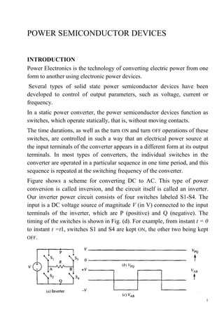
  • 1. 1 POWER SEMICONDUCTOR DEVICES INTRODUCTION Power Electronics is the technology of converting electric power from one form to another using electronic power devices. Several types of solid state power semiconductor devices have been developed to control of output parameters, such as voltage, current or frequency. In a static power converter, the power semiconductor devices function as switches, which operate statically, that is, without moving contacts. The time durations, as well as the turn ON and turn OFF operations of these switches, are controlled in such a way that an electrical power source at the input terminals of the converter appears in a different form at its output terminals. In most types of converters, the individual switches in the converter are operated in a particular sequence in one time period, and this sequence is repeated at the switching frequency of the converter. Figure shows a scheme for converting DC to AC. This type of power conversion is called inversion, and the circuit itself is called an inverter. Our inverter power circuit consists of four switches labeled S1-S4. The input is a DC voltage source of magnitude V (in V) connected to the input terminals of the inverter, which are P (positive) and Q (negative). The timing of the switches is shown in Fig. (d). For example, from instant t = 0 to instant t =t1, switches S1 and S4 are kept ON, the other two being kept OFF.
  • 2. 2 Therefore the input DC voltage appears at the output terminals with terminal A positive. During the next interval from S1 and S4 are kept OFF, but S2 and S3 are kept ON. Therefore, during this interval, the input DC voltage appears at the output terminals with reversed polarity (A negative). This sequence of switching is repeated, and in this way the input voltage V of fixed polarity shown in Fig.(b) is presented at the output terminals PQ as an AC square wave voltage as shown in Fig. (с). Figure (e) shows how the same circuit configuration of four switches can be used to convert an AC voltage source connected at the terminals AB into a DC voltage at the terminals PQ. This type of power conversion is called rectification, and the circuit itself a rectifier. In our rectifier of Fig. (e), the switches S1-S4 are operated according to the same timing as indicated by Fig. (d). The input terminals of the rectifier are now A and B, to which the AC square wave voltage such as that shown in Fig. (c) is connected. The output terminals of our rectifier are P (positive) and Q (negative). The input AC voltage is now presented as a unidirectional voltage at the output terminals. Notice that the directions of current through the switches will be different in Figs (a) and (e). The objective of this course is to present the principles underlying power conversion by the use of static switches and the techniques employed for controlling output parameters such as voltage, current, power, frequency and waveform. We shall, in a progressive sequence, present all the important types of power converters that have proved useful in the application areas of electric power. We shall also present important application areas, and this will bring out how converter schemes and control strategies can be tailored to meet specific needs.
  • 3. 3 TYPES OF STATIC SWITCHES 1. Uncontrolled Static Switch—The Power Diode The simplest static switch is the diode. A power diode is a two-terminal device, whose circuit symbol is shown in Fig. (a). An ideal diode conducts when forward-biased, with negligible voltage drop across it and a forward current, IF, flows through it. If, however, it is reverse-biased, ideally, it does not conduct. A real diode will have a small forward voltage drop across it when it conducts and a small reverse leakage current when it is reverse-biased. The diode switch blocks reverse voltages, but has no capability to block forward voltages. We can describe the ideal power diode as an uncontrolled static switch that turns ON and turns OFF by itself, depending on the polarity of the voltage. 2 Controlled Switch A controlled switch is one that could be turned ON and OFF by activating and deactivating a control circuit. Figure 1.2(b) shows a nonstatic (with moving contacts) switch of this kind. It has a control coil whose terminals are labeled C1 and C2. The power terminals of the switch are labeled 1 and 2. To turn ON this switch, we send a current through the control coil, which will cause the plunger to move and connect the power terminals. The following aspects should be noted here. 1. The switch has four terminals—two for the power circuit and two for the control circuit. 2. The control circuit is electrically isolated from the power circuit. The electrical isolation between the power terminals and the control circuit
  • 4. 4 is very often a requirement in static power converters. Unfortunately, power semiconductor switching devices presently available do not provide any isolation at all between the power and control terminals. In fact, every power semiconductor switch is a three-terminal device. A typical example is the power transistor. The power terminals are the collector and the emitter. The third terminal, namely the base, and the emitter are the control terminals. The circuit symbol that we shall use to represent an ideal three- terminal controlled unidirectional static switch is shown in Fig. (c). The power terminals of the switch are labeled 1 and 2. The arrow shows the direction of ON state current through it. The control input is across terminals С and 1. 3 Directional Properties of Static Switches—Current Direction The power diode is a static uncontrolled switch with only one direction for current flow. The general circuit symbol that we have chosen and shown in Fig. 1.2(c) is for a controlled switch, which is also unidirectional. The unidirectional the power semiconductor switches are, 1. the power diode, 2. the bipolar power transistor, 3. the insulated gate bipolar transistor (IGBT), 4. the thyristor, also known as the silicon controlled rectifier (SCR), 5. the asymmetrical silicon controlled rectifier (ASCR), 6. the gate turn off thyristor (GTO) 7. the MOS controlled Thyristor (MCT). The switches with bi-directional current capability are: 1. the power MOSFET, 2. the reverse conducting thyristor, 3. the triac. Of these, the power MOSFET and the reverse conducting thyristor function as controlled switches in the forward direction and as uncontrolled switches in the reverse direction Fig. (d). The triac works as a controlled switch in both directions.
  • 5. 5 4. Directional Voltage Capabilities of Static Switches A distinction must be drawn between directional current flow capability and directional voltage blocking capability for a static power semiconductor switch. The bipolar power transistor is a static switch that can only switch current in the "forward" direction. This does not mean that it has ability to block reverse voltages. In contrast, the thyristor, which is also a unidirectional switch, has a symmetrical voltage blocking capability in that it can block approximately the same voltages in both forward and reverse directions. TABLE 1 Properties of power semiconductor switching devices TypeofForwardON switchingControl Iscontrolavailablefor switchingOFFF.current? Iscontrolavailableforreverse conduction? Iscontrolavailablefor switchingOFFR.current? CapabilitytoblockF.Voltage CapabilitytoblockR.Voltage Reversecondition C+ L+ C L С L С L Power diode No Yes No No control Bipolar power transistor Yes No No Yes Yes Not Power MOSFET Yes No Yes Yes Yes No No Insulated Gate Bipolar Transistor (IGBT) Yes No No Yes Yes N/A Thyristor (SCR) Yes Yes No Yes No N/A Asymmetrical SCR Yes No No Yes No N/A Reverse conducting thyristor Yes No Yes Yes No No No Gate turn off thyristor (GTO), reverse blocking type Yes Yes No Yes Yes N/A GTO without reverse voltage blocking capability Yes No No Yes Yes N/A Triac Yes Yes Yes Yes No Yes No MOS controlled thyristor Yes No No Yes Yes N/A
  • 6. 6 5. Types of Switching Control — Continuous or Latching There is a major difference between static switches in the manner in which the control terminal performs the switching operation. In some devices, such as the bipolar power transistor and the power MOSFET, after the turn ON switching is implemented by an input to the control terminal, this input should continue to be present, to keep the switch in the ON state. If the control input ceases, the switch will turn OFF. With such a switch, both the turn ON and the turn OFF operations can be implemented by the same control circuit. This type of control may be described as "continuous". In devices like the thyristor, the control input to implement turn ON need be only a pulse of very short duration. Once the switch has turned ON, there is no further need for the turn ON control pulse to be present. Another example of this type of control is the gate turn OFF thyristor (GTO). The GTO is turned ON by a short positive pulse and turned OFF by a short negative pulse on its control terminal. This type of control may be described as "latching", because the device is latched into the required state by a pulse of short duration. The thyristor, which is a latching device, has a serious limitation. Its control terminal (gate) has the ability only to control the ON switching operation. Once the device has been latched into the ON state, the gate loses control and the device behaves like a diode. Its OFF switching has to take place by reverse bias of the main terminals like a diode.
  • 7. 7 Ideal and Real Switches To assess the performance of a switch, we look at two aspects of its behavior—static and dynamic. If the switch is either in its ON or OFF state, we call this a static condition. The dynamic condition is the transition from one static state to the other. 1. Static Performance An ideal switch should have zero voltage across it in the ON state and zero current through it in the OFF state when it is blocking a voltage. The product of current and voltage, which gives the power dissipated in the switch, is zero in both conditions. This is the basic reason why a power conversion scheme based on switching is more efficient than other methods, because ideally, there is no internal power loss. Power semiconductor switches depart to some extent from the ideal— there is a small but finite voltage drop in the ON state and a small but finite "leakage current" in the OFF state. The power dissipated in a switch during its ON state is given (in W) by ff vip ⋅= For an ON period duration t1 to t2,, during which Vf and if may vary, the total energy (in J) dissipated in it will be dtviJ t t ff ⋅⋅= ∫ 2 1 Energy dissipated in the switch causes its temperature to rise. The efficiency of power conversion is also lowered, because of the power dissipation in the switches. The leakage current that flows in the OFF state causes the power dissipation in the device. Usually the power dissipation due to this leakage current is small in comparison with the power dissipation in the ON state therefore the power dissipation due to OFF state leakage can be neglected.
  • 8. 8 2 Dynamic Performance An ideal switch should change from the OFF state to the ON state, instantaneously, when the required switching control signal is applied to its control terminal. Similarly, the transition time for the turn OFF switching should also be zero. A real switch needs a finite ton for ON switching and tof for OFF switching. These finite switching times have two major consequences. 1. They limit the highest repetitive switching frequencies possible. 2. They introduce additional power dissipation in the switches themselves. Of these, the second phenomenon needs further explanation. Instantaneous voltages, currents and power in a static switch during the switching transitions. Figure shows the waveforms of (1) the voltage drop across the switch and (2) the current I through it, when a turn ON switching is implemented at t =t1 and a turn OFF - switching at t = t2.
  • 9. 9 We notice that during the transition there is power dissipation taking place inside the switch, whose instantaneous value is given by the product of voltage and current. The instantaneous power is also plotted (3) as a function of time in Fig. Depending on the nature of the current and voltage waveforms during the transition, the peak power can reach a relatively large magnitude. The energy dissipation in the switch is equal to the area shown hatched under the power waveform. The total energy J (in J) dissipated in the switch in one switching cycle is given by the sum of the areas under the power waveform during ton and toff. The average switching power loss is therefore proportional to the switching frequency, and is given (in W) by JfPswitching ⋅= f being the converter switching frequency (in Hz). 3. Temperature Rise—Use of Heat Sinks The immediate consequence of energy dissipation in a static switch is its temperature rise. The need for cooling arises to keep the switch temperature below its safe limit. The exact location where the heat is generated is in the silicon pellet that actually is the switch. Electrical contacts are made to appropriate areas of this thin wafer, and these constitute the terminals of the device, which are brought outside the casing in which the silicon pellet is housed. The power losses of the switch raises the temperature of the pellet. The temperature gradient thus created causes the heat power to flow outwards to the casing surface. To facilitate the easier flow of heat power to the ambient atmosphere outside, it is a common practice to mount the casing on a "heat sink." Heat sinks are made of metal, and provide a large surface area from which the heat power can pass by convection and radiation to the ambient atmosphere. The convection flow can be further enhanced, if needed, by using a fan to provide forced air cooling.
  • 10. 10 With the device mounted on a heat sink, the path of heat flow can be viewed as a series combination of the following individual paths: (1) from the junction (J) to the surface of the casing (C); (2) from the surface of the casing (C) to the outer surface of the heat sink (S); (3) from S to the ambient atmosphere (A), which we shall assume to be an external region sufficiently distant from the heat sink, at which the thermal gradient is negligible. With constant power dissipation inside the pellet, thermal equilibrium conditions will be attained after a period of time. After this has happened, the temperatures and temperature gradients stay constant in such a way that all the power dissipated inside the device continually flows out into the ambient. Taking thermal power flow as proportional to temperature difference, we can represent this condition by an electrical analog in which electric current (in A) represents thermal power (in W) and potential difference (in V) represents temperature difference (in °C). Such an analogous electric circuit will consist of resistances (Ω = V/A) as the analog of "thermal resistance" (expressed as o C/W). On this basis, Fig. 1.8 shows the thermal power flow model for a static switch mounted on a heat sink. In this model, J represents the inside of the silicon pellet. ΘJC is the thermal resistance (in °C/W) between J and the outer surface of the casing C. The other thermal resistances are labeled by appropriate subscripts. This model can be used to make estimates of the junction temperature rise when the power dissipation is known, or to estimate the maximum power dissipation possible for a specified junction temperature.
  • 11. 11 POWER DIODES 1 Available Ratings, Types Diodes employed in static converters are essentially high power versions of conventional low power devices used in analog and digital signal processing circuits. Power diodes are manufactured in a wide range of current and voltage ratings. Current ratings vary from a few amperes to several hundred amperes. Voltage ratings extend from tens of volts to several thousand volts. The important parameter is its "reverse recovery time." – a time after the forward conduction which is necessary to recover its ability to block reverse voltages. Based on this time, diodes are classified as "fast recovery" and "slow recovery" types. Certain types of converters require the use of fast recovery power diodes. 2. Junction Structure, Packaging The diode consists of a silicon pellet with a single internal pn junction [Fig. (a)]. Typically, it is fabricated by diffusing p- type impurity atoms into one side of a n-type crystal wafer of silicon. It has two terminals, of which the anode (A) makes contact with the p side surface of the pellet and the cathode (K) with the n side. The forward direction of current flow is from A to K, as shown by the diode circuit symbol [Fig. (b)]. The power diode: junction structure, circuit symbol and package types.
  • 12. 12 The area of the pellet determines the current rating. For example, a large area device using a silicon wafer of 4 in. diameter may have a current rating of 1000 A. The resistivity of the starting material and its thickness are mainly responsible for the voltage blocking capability of the device - its voltage rating will go up with the purity level of the starting wafer and its thickness. The impurity profile in the silicon pellet has a major effect on both its ON state forward voltage drop and also on its reverse recovery time. A trade off exists between blocking voltage capability and reverse recovery time. High resistivity silicon has a long minority carrier lifetime. A trade off also exists between blocking voltage capability and ON state forward voltage drop. If a thicker and higher resistivity wafer is employed to achieve higher voltage rating, this will result in a higher forward voltage drop in the ON state. There are two types of packages commonly used for housing the diode pellet. In the stud type package shown in Fig. (c), the casing, which is of metal, has a threaded stud for easy mounting on a heat sink. The metal casing and the stud constitute one terminal of the diode. The other terminal is brought out on the side opposite to the stud, with electrical insulation from the casing. Stud-type diodes are available with either polarity for the stud—anode or cathode. By choosing the stud polarity of the diode to match the casing terminal of the controlled switching device, both devices can be mounted on the same heat sink. Diodes with very large current and voltage ratings employ the disc package, also known as "hockey puck," illustrated in Fig. (d). Here, the two terminals are flat metallic surfaces separated by a ceramic insulator. Disc-type diodes are mounted with at least one side in contact with a flat heat sink surface. For better cooling, two separate heat sinks may be used—one on each side. Special mounting hardware, which provide for adequate contact pressure and insulation between the two sides is usually available from the manufacturer.
  • 13. 13 3 Reverse Recovery Characteristics For most practical purposes, we can consider the turn ON switching of a diode as instantaneous. But the turn OFF switching behavior requires special consideration, because this has a significant effect on the performance of most types of static converters. Let us assume that S has been ON for a long time, as a result of which a current has been established in the R-L circuit. After this, S в turned OFF. But the current in the R-L circuit cannot instantly fall to zero, because of the presence of the inductance L. When the current tends to fall, the induced e.m.f. in the inductance will forward-bias the diode, and the current, will "freewheel," that is, continue to flow through it due to the stored energy in the inductance, even though there is no voltage source present to drive this current. We shall assume that L is large, so that the decay of current is negligible during the short period of our next sequence of observations. In other words, / will be assumed to be constant. 1. From t = t0 to t = t1 in Fig. (b), when S is turned ON again. This will cause a current is to build up in the DC source and through switch S. We will assume that the rate of increase of is is constant. This rate di/dt is determined by the residual inductance in the circuit mesh consisting of the source, the diode D and S. Since I is constant, the increase in is results in an equal decrease in the diode current id: Iii ds =+ Therefore dt i dt i sd −= This linear fall of current in the diode is shown by the diode current waveform in Fig. (b).
  • 14. 14 2. From t = t1 to t = t2 If the diode is ideal in its dynamic behavior, it should stop conducting at t =t1 and recover its reverse voltage blocking ability. But, because of the excess minority carriers it continues to conduct after t = t1, now in the reverse direction. Therefore the diode continues to be a conducting switch and the current waveform continues unaffected, until the excess carriers are removed. This happens at t = t2. 3. From t = t2 to t = t3 After t = t2 the reverse current falls towards zero and the diode recovers its reverse voltage blocking capability. In the reverse blocking condition, the diode is charged to the reverse voltage. The diode current falls to zero at t = t3, when this junction capacitance has been charged to the full reverse voltage. At this instant, the turn OFF switching transition of the diode is complete. The "reverse recovery time" tr is the time interval measured from the instant at which the forward current has fallen to zero to the instant at which the reverse voltage recovery is completed. The specified reverse recovery time in the data sheet of a power diode is correct only for the specified test conditions. It does vary to some extent, depending on the test conditions, and is higher for a larger ON state current before the commencement of turn OFF. If this time is very short, the diode is described as belonging to the "hard recovery" category. If this interval is relatively long, it is a "soft recovery" type. It follows that a soft recovery diode has a lower di/dt during reverse recovery. Soft recovery diodes are generally preferable in static power converters, because inductive voltage spikes resulting from the diodes' reverse recovery transients, are smaller.
  • 15. 15 EFFECTS OF REVERSE RECOVERY TRANSIENT 1 High Currents In The Controlled Switches. In DC/DC converters and DC/AC inverters, when S is repetitively turned ON and turned OFF in each switching cycle, there is a current transfer taking place at each switching, between S and the diode. If the diode were ideal, with no reverse recovery current, S would have to carry only the output current in the R-L circuit. In the real situation S has to handle the sum of the output current and the reverse recovery current immediately after it is turned ON. This means that it should be capable of carrying a pulse current of very large amplitude and of dissipating the additional power due to this current spike. Alternatively, the amplitude of the current pulse itself should be limited by inserting additional inductance in series with the source. 2 Over-Voltage Spike Across Diode. Any inductance present in the loop causes a voltage spike to appear across the diode, during the decay of the reverse current. The magnitude of this reverse over-voltage spike depends on the loop inductance value and the slope di/dt of the reverse current. In a real diode, the di/dt value during the decay of reverse current is not constant, as we have assumed by the approximated straight line from t2 to t3. Therefore, the reverse over- voltage varies and has a peak value during this interval. 3 Limitation Of Converter Switching Frequency. In a static converter, if the switching frequency is increased, the recovery time tr of the diodes will constitute an increasing fraction of the total cycle time. This will generally decrease the efficiency of the converter. Therefore the reverse recovery time sets an upper limit to the converter switching frequency.
  • 16. 16 Schottky Diodes Schottky diodes do not have a pn junction. Instead, they employ a metal- to-silicon barrier. In a Schottky diode, the current flow is due to the flow of majority carriers. Therefore they are suitable for use at very high frequencies. The barrier does have a capacitance, which accounts for a certain amount of reverse current, to charge this capacitance to the reverse voltage. Current ratings of Schottky diodes available are well below 100 A. Reverse voltage ratings are well below 100 V. They are very widely used in "switch mode power supplies," which work at high switching frequencies. Snubber Circuits (Switching Aid Circuits) A snubber circuit for a diode serves to protect it from damage that can arise due to an over-voltage spike during reverse recovery. During the decay of the reverse recovery current, the capacitor serves to limit the voltage spike. Snubber Circuits Series Operation of Diodes Series and Parallel Operation of Diodes When the voltage rating of an available diode type is not high enough for a high voltage application, several such diodes connected in series can be used to achieve the required voltage capability. If this is done, it is necesssary to ensure that each diode in the series chain shares the total reverse voltage nearly equally. To achieve high current capability, several diodes of one type can be connected in parallel. The recommended practice is to choose diodes that are matched as regards forward voltage drop.
  • 17. 17 CURRENT AND VOLTAGE RATINGS OF POWER DIODES 1 Current Ratings. The data sheet of a power diode usually gives three separate types of current ratings: (1) the average current, (2) the r.m.s. current and (3) the peak current. It is important to ensure that none of these ratings is exceeded in actual operation. To explain the significance of each of these ratings, we shall use the current waveform shown bellow. AIaverage 101/2.050 =×= [ ] AIrms 4.221/2.0502 =×= AI peak 50= 2 VOLTAGE RATINGS. For high power diodes, the data sheets usually specify two voltage ratings: (1) the repetitive peak reverse voltage and (2) the nonrepetitive peak reverse voltage. The non-repetitive peak is specified to indicate the capability of a diode to withstand an occasional over- voltage surge that may occur due to a circuit fault. VVVV rmsBNpeakANpeak 1702120 ≈== Total peak reverse Voltage is 2 x 170V= 340V