1. GeSn Photodetectors:
Ø Advantages: higher optical absorption in 1.3-1.55 µm wavelength range
than Si
Ø Challenges: narrow bandgap and surface defects (dangling bonds) cause
high dark current that reduce device sensitivity
Ø Goal: compare passivation methods to minimize dark current
C.E. Brendel*, M. Morea, J.S. Harris
Stanford University: Electrical Engineering Department
Fabrication and Characterization of Low Dark-Current GeSn Photodetectors
References:
1) Micromanipulator 6000. The MicroManipulator Co. Inc., n.d. Web. 22 Aug 2016.
All other photos and figures created by researchers of this project.
From left to right:
Corinna Brendel, Matthew Morea, Dr. James S. Harris
*Correspondence should be addressed to:
Corinna Brendel, cbrendel@stanford.edu
Acknowledgements:
1) Project organized by Stanford EE – REU Program
2) Atomic Layer Deposition done in part at CIS-111x Lab with assistance from Junkyo Suh of the Saraswat Group
3) Access to photocurrent measurement setup granted by Dr. Jorik van de Groep of the Brongersma Group
4) Part of this work was performed at the Stanford Nano Shared Facilities (SNSF)
Si substrate
i-Ge buffer
i-Ge spacer
i-GeSn well (3% Sn)
i-Ge barrier
i-GeSn well (3% Sn)
i-Ge barrier
i-GeSn well (3% Sn)
i-Ge spacer
p+ Ge contact (1x1019 cm-3)
n+ Ge (180 nm, 1x1019 cm-3)
35nm
35nm
35nm
35nm
35nm
35nm
500nm
1µm
180nm
35nm
SiNx
Au
Au Au
2 µm
PR Removal
Ø gasonics, wbsolvent (1165, acetone,
IPA), drytek2 descum
Clean wafers
Ø wbsolvent w/ N2 gun, SRD
Layer 0 Etch
Ø pt-mtl, 250nm Ge
SiNx Hard Mask
Ø wbflexcorr clean (BOE, N2)
Ø ccp, 350nm SiN
Layer 0 Litho
Ø Alignment mask
Layer 1 Litho
Ø Mesa mask
Mid-Process Passivation
Layer 1 Etch (pattern transfer, mesa etch)
Ø pt-ox, 350nm SiN
Ø pt-mtl, 900n Ge
Layer 2 Litho
Ø Via mask
Layer 2 Etch (open vias)
Ø pt-ox, 250nm SiN
Layer 3 Litho
Ø dual-layer PR coat, headway2 (LOL2000)
Ø Metal mask
Metal Contact Formation
Ø metalica deposition (10nm NiCr, 200nm Au)
Ø wbsolvent, Lift-off Process
Post-Process Passivation
Development
PR Coat
Ø svgcoat (1.0um SPR3612), SRD
Ø ASML exposure, bake, svgdev
PR Treat
Ø drytek2 descum
General Litho Step
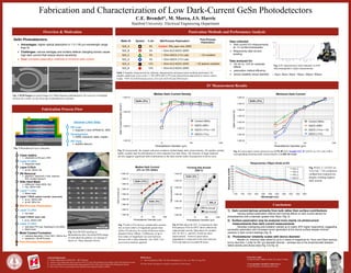
Fig. 3 (a) DI-H2O pooling on
photodetector dies, (b) aerial SEM image
of individual die patttern, (c) closeup of
layers on 50µm diameter device
Fig. 2 Photodetector layer schematic
1) Dark current derives primarily from bulk rather than surface contributions
Varying surface passivation method had minimal effects on dark current density for
photodetectors with a diameter greater than 50µm (Fig. 5)
2) Surface passivation may be analyzed more clearly via photocurrent
measurements than dark current measurements
Samples undergoing post-oxidation yielded up to nearly 30% higher responsivity, suggesting
successful passivation and increased carrier generation at the device surface despite minimal
variance in dark current readings (Fig. 9)
3) Photodetector reliability scales with device diameter
Median vs. minimum data varied by up to 2 orders of magnitude for 10µm and 20µm devices,
but by less than 1 order for 50+ µm diameter devices – perhaps due to the proportionality between
defect density and device area (Fig. 5 & Fig. 6)
Conclusions
Wafer ID Symbol % Sn Mid-Process Passivation*
Post-Process
Passivation
S22_A 3% Control: SiNx layer only (SNF) -
S22_B 3% • 10nm ALD Al2O3 (SNF) -
S22_C 3% • 10nm Al2O3 (111x Lab) • O3 oxidation
S22_D 3% • 10nm Al2O3 (111x Lab) -
S23_A 12% • 10nm ALD Al2O3 (SNF) • O2 plasma oxidation
S23_B 12% • 10nm ALD Al2O3 (SNF) -
Data collected:
Ø Dark current (IV) measurements
at -1V via Micromanipulator
Ø Responsivity data via wire
bonding
Data analyzed for:
Ø 3% Sn vs. 12% Sn substrate
effects
Ø passivation method efficiency
Ø device reliability versus diameter
Passivation Methods and Performance Analysis
Table 1 Samples characterized by substrate characteristics and passivation methods performed. All
samples underwent a two cycle 1:1 HF (49%) HCl (37%) pre-clean before deposition to remove native
oxides. *SNF ALD H2O based versus 111x Lab ALD O3 and TMA based
Fig. 4 IV characteristics (left) obtained via SNF
Micromanipulator (right) measurements
Fig. 1 SEM Images (a) aerial image of a 50µm diameter photodetector, (b) overview of multiple
devices on a wafer, (c) (d) close-ups of photodetector structure
a b c
d
a
b
c
0
20
40
60
80
100
120
140
160
180
200
1100 1150 1200 1250 1300 1350 1400 1450 1500 1550 1600
Responsivity(mA/W)
Wavelength (nm)
Responsivity (100µm Diode at 0V)
S22_A
S22_B
S22_C
S22_D
Fig. 9 S22_C (Al2O3 via
111x Lab + O3 oxidation)
yielded best responsivity
despite yielding highest
dark current.
1.00E-08
1.00E-07
1.00E-06
1.00E-05
1.00E-04
1.00E-03
1.00E-02
1.00E-01
1.00E+00
1 10 100 1000
DarkCurrent(A)
Photodetector Diameter (µm)
Median Dark Current
(3% vs 12% GeSn)
GeSn (12%)
GeSn (3%)
1.00E-08
1.00E-07
1.00E-06
1.00E-05
1.00E-04
1.00E-03
1.00E-02
1 10 100 1000
DarkCurrent(A)
Photodetector Diameter (µm)
Forming Gas Anneal
(250 C)
Pre-Anneal
Post-Anneal
GeSn (3%)
Fig. 7 GeSn (12%) devices yielded dark currents
two or more orders of magnitude greater than
GeSn (3%) devices for nearly all devices with a
diameter below 200µm. A difference of up to
four orders of magnitude was seen between
devices with a 10µm diameter. (see Table 1 for
passivation methods applied)
Fig. 8 Data taken for S22_A immediately after
Post-process FGA at 250 C shows effectively
reduced dark current. Data taken for samples
S22_B, S22_C, and S22_D did not show
improvement – however passivation
degradation is suspected as the time between
FGA and analysis exceeded 48 hours.
S22_A
-- 10µm, 20µm, 50µm, 100µm, 200µm, 500µm
Fabrication Process Flow
Overview & Motivation
IV Measurement Results
Fig. 5 Unexpectedly, the sample with post-oxidation yielded higher dark current density. All samples yielded
highly variable data for photodetectors with a diameter less than 50µm. The linearity of larger diameter
devices suggests significant bulk contributions as the dark current scales in proportion to device area.
Fig. 6 Lowest dark current achieved was 3.37E-09 A for Sample S22_D (Al2O3 via 111x Lab) with a
corresponding minimum dark current density of 4.28E-03 A/cm2.
1.00E-02
1.00E-01
1.00E+00
1.00E+01
1 10 100 1000
DarkCurrentDensity(A/cm2)
Photodetector Diameter (µm)
Median Dark Current Density
Control (SiNx)
Al2O3 (SNF)
Al2O3 (111x) + O3
Al2O3 (111x)
1.00E-09
1.00E-08
1.00E-07
1.00E-06
1.00E-05
1.00E-04
1.00E-03
1.00E-02
1 10 100 1000
DarkCurrent(A)
Photodetector Diameter (µm)
Minimum Dark Current
Control (SiNx)
Al2O3 (SNF)
Al2O3 (111x) + O3
Al2O3 (111x)
GeSn (3%) GeSn (3%)