Tem Crams of Distinctive NLO Material (Second Harmonic Generative Type) Bariu...
Adrianne diamond doping poster
1. References
http://awsch-
web.physics.ucsb.edu/research/solid_state/pnas_defe
cts/pnas_defects_01.jpg
Romana Schirhagl, Kevin Chang, Michael Loretz,
and Christian L. Degen, 2014, Optically Detected
Magnetic Resonance, Nitrogen-Vacancy Centers in
Diamond: Nanoscale Sensors for Physics and
Biology, Annual Reviews, Z ¨ urich, Switzerland
In six years the size of transistors will reach four
nanometers and ultimately their size and speed limit.
To further increase device performance, quantum
mechanics may hold the answer by manipulating the
spin of electrons. The most stable way to obtain
these electrons is by forming nitrogen-vacancy
centers (NV-Center) in a crystal lattice structure
through a process called doping. Using a hot filament
chemical vapor deposition (HFCVD) system, the
samples were grown and the attempt to successfully
dope was practiced. NV-Center characterization by
confocal microscopy was insufficient in determining
any presence.
Abstract
Adrianne Hargrove, Dr. Gary Harris, Mr. James Griffin, Ms. Bokani Mtengi
Howard Nanoscale Science and Engineering Facility, Howard University, DC
Acknowledgments
Howard University Nano-Technology Lab
Mentors: Mr. James Griffin and Bokani Mtengi
PI: Dr. Gary Harris
CIQM – Dr. Brower-Thomas
National Institute of Standards and Technology
Doping Nano Diamonds
DMR-1231319
Crystal lattice structure with a
nitrogen vacancy center (NV- Center)
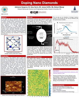
Results and Discussion
The doped nano diamond samples were tested
through the process of confocal microscopy at the
National Institute of Standards and Technology. On
the vertical scale, red indicates a higher intensity than
blue. For this particular sample, the nitrogen applied
to the diamond sample was 53% of the total flow rate;
the highest percentage used out of all the
experiments.
The objectives of this research were to grow and
characterize nano diamonds as well as doped nano
diamond. The characterization of the nano diamond
was performed through atomic force microscopy and
scanning electron microscopy. Once twelve samples
where completed the next goal was to dope them
with Nitrogen. The doped nano diamonds were then
characterized through the process of confocal
microscopy. The nitrogen doping is performed to
obtain NV- centers in a crystal lattice structure. The
vacancies which contain radical electrons will then
become exposed to microwaves or light in order to
manipulate the electron spin and ultimately store and
process information at faster speeds than modern
transistors.
Introduction
The red dots are an indication of nitrogen vacancy
centers in the sample but can not be confirmed until
the spectroscopy is viewed .
As shown above, the spectroscopy of an NV- center
should display a distinct peak at 638nm and a gradual
decline between 630and 800nm (blue graph) for a
single crystal diamond. Our sample (red graph),
which is polycrystalline, resulted in countless peaks,
none of which were distinct at the wavelength
specified. The spectrum reflected several broad
peaks which are characteristics of defects within the
materials and could also possibly be NV-centers.
A hot filament chemical vapor deposition system was
used to grow the nano diamond on a silicon wafer.
The filament was set to a temperature of 2300°C
where it was able to break the methane and di-
hydrogen bond to grow the synthetic diamond.
Methods
For the doping process, Nitrogen was put into the
HFCVD after growth. The filament temperature was
raised to 2500°C in an attempt to break the strong
bond nitrogen has with itself. Multiple experiments
were ran that changed the amount of nitrogen
entering the chamber, the methane flow rate, and the
growth time.
Atomic force microscopy image of nano diamond