IP PCIe
•
1 like•1,198 views

The document describes an AXI_PCIEX1 module that acts as a PCI Express to AXI bridge, allowing a system with an embedded AXI bus to connect to an external PCI Express bus. The module is compliant with DO-254 guidance for critical applications and has a low gate count and latency. It supports PCIe 1.0 at 2.5 Gbps on one lane and interfaces with AXI4 at 32 bits. The module is optimized for reliability and error reporting. DMAP provides Verilog RTL, verification testbenches, and all required certification documentation.

Recommended
More Related Content
What's hot
What's hot (20)
Viewers also liked
Viewers also liked (15)
Similar to IP PCIe
Similar to IP PCIe (20)
More from SILKAN
Recently uploaded
Recently uploaded (20)
IP PCIe
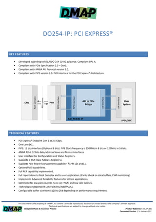
- 1. DO254-IP: PCI EXPRESS® KEY FEATURES Developed according to RTCA/DO-254 ED-80 guidance. Compliant DAL A. Compliant with PCIe Specification 2.0 – Gen1. Compliant with AMBA AXI Protocol version 2.0. Compliant with PIPE version 1.0. PHY Interface for the PCI Express® Architecture. Root Complex PIPE Interface PIPE Interface AXI Interface AXI Interface PCI Express AXI to PCIe User CPU PHY Bridge System AXI_PCIEX1 IP FPGA/ASIC TECHNICAL FEATURES PCI Express® Endpoint Gen 1 at 2.5 Gbps. One Lane (x1). PIPE: 16 bits interface (Optional 8 bits). PIPE Clock frequency is 250MHz in 8 bits or 125MHz in 16 bits. AMBA AXI4: 32 bits data/address Slave and Master Interfaces User interface for Configuration and Status Registers. Supports 6 BAR (Base Address Registers). Supports PCIe Power Management capability: ASPM L0s and L1. Optional MSI capabilities. Full AER capability implemented. Full report done to Root Complex and to user application. (Parity check on data buffers, FSM monitoring) Implements Advanced Reliability features for critical applications. Optimized for low gate count (4-5k LE on FPGA) and low core latency. Technology independent (Altera/Xilinx/Actel/ASIC). Configurable buffer size from 512B to 2kB depending on performance requirement. This document is the property of DMAP®. Its content cannot be reproduced, disclosed or utilized without the company's written approval. Technical specifications are subject to change without prior notice Design Methods & Assurance Process Product Reference: AXI_PCIEX1 Document Version: 1.3– January 2011
- 2. OVERVIEW The AXI_PCIEX1 module is a PCI Express® to AXI Bridge. It allows a system with an embedded AXI bus to be connected to an external PCI Express® Bus. The hardware item only covers digital layers of the PCI Express® bus architecture. In a typical system the main external processor is able to address the internal AXI bus used to interconnect all internal components all together. With its unique internal architecture the digital core is optimized for low gate count and low latency applications. The AXI_PCIEX1 is able to recover from SEU and to report any detected errors with the help of its embedded reliability features. Detected errors are then reported to external processor and to internal sub-system. The AXI_PCIEX1 matches major needs of any critical application and mainly those which require a DO-254 DAL-A compliance in the aerospace area. The development has been done according to the RTCA/DO-254 ED-80 guidelines. This component has been developed, verified and licensed by DMAP. DELIVERABLES Technology independent Verilog RTL sources code compliant with DMAP’s design standard. SystemVerilog Functional verification test-benches using best-in class BFM from Mentor Graphics with full code and functional coverage. Reference Design as integration example (Dry Run) on Xilinx device. DMAP’s support includes technical integration, DO-254 integration and certification phases. IP Datasheet and Customer Requirement Specification (CRS) document. It includes all required data for RTCA/DO-254/ED-80 certification, including configuration management records, change management records and assurance process records: Hardware Planning Process: Hardware Development Plan (HDP), Hardware Validation and Verification Plan (HVVP), Hardware Configuration Management Plan (HCMP), Hardware Process Assurance Plan (HPAP) and Plan for Hardware Aspects of Certification (PHAC). Standards: Hardware Requirement Standard (HRS), Hardware Design Standard (HDS). Hardware Development Process: Hardware Requirement Document (HRD), Hardware Conceptual Document (HCD), Hardware Detailed Document (HDD), Hardware Traceability Matrixes (HTM), Hardware Accomplishment Summary (HAS) and Hardware Software Interface Document (HSID). Hardware Verification and Validation Process: Hardware Verification Cases Procedures (HVCP) and Hardware Verification Results (HVR) and validation activities reports. Project Review: Initial Design Review (IDR), Preliminary Design Review (PDR), Critical Design Review (CDR) and Final Design Review (FDR). Hardware Configuration Management Process: Hardware Configuration Index (HCI), Hardware Environment Configuration Index (HECI). CONTACT Product Reference: AXI_PCIEX1. DMAP Email: contact@dmap.fr For further product’s information and other DMAP’s Web: http://www.dmap.fr services please contact: Phone: +33(0)4 42 61 29 13 100, route des Houillères, 13590 Meyreuil, France. This document is the property of DMAP®. Its content cannot be reproduced, disclosed or utilized without the company's written approval. Technical specifications are subject to change without prior notice Design Methods & Assurance Process Product Reference: AXI_PCIEX1 Document Version: 1.3– January 2011