18. Best Practices:
VCC should be connected via a star-like formation to sub
systems, with branches of equal length, NOT in a cascaded
or serial way where the last sub system is furthest away
from VCC. This will make the later sub systems vulnerable
to noise produced by the upstream ones.
:( :)
19. Best Practices:
-minimize trace lengths, components electronically close
should be physically close too. Longer traces have higher
resistance, capacitance and inductance.
:(
:)
20. Best Practices:
-Think in terms of a signal chain, with input on the left
moving towards output on the right. Divide things into
building blocks. Build each block separately and then throw
it on the main board.
Abstraction +
decomposition
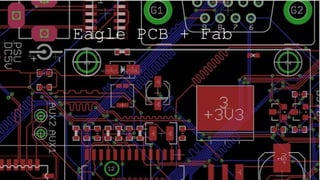
25. Board
https://cdn.sparkfun.com/assets/e/6/f/e/2/52051bb3757b7fad144bb8e4.png
Place edge components first, things like USB
ports, power jacks, headers, etc… And make
sure that decoupling capacitor is nice and
close to the IC.
Don't overlap parts: All of your components
need some space to breathe.
Limit criss-crossing airwires
Tighter placement means a smaller and cheaper
board, but it also makes routing harder
26. Board
Design Rules Check (DRC) checks for:
Clearance: A trace is too close to either another trace or a
via. You'll probably have to nudge the trace around using the
MOVE tool.
Overlap: Two different signal traces are overlapping each
other. This will create a short if it's not fixed. You might
have to RIPUP one trace, and try routing it on the other side
of the board. Or find a new way for it to reach its
destination.
Dimension: A trace, pad, or via is intersecting with (or too
close to) a dimension line. If this isn't fixed that part of
the board will just be cut off.
Etc.
47. Reverse Polarity protection
A P-Channel MOSFET set up where the gate is
connected to ground will only turn on when the
polarity is correct. If Vin is not greater than the
maximum allowed voltage you can put accross the
MOSFET from gate to source (Vgs max.), or the Vin is
not less than the threshold required for the P-FET
to turn on (Vgs th), then it doesn’t need any other
components.
48. Overvoltage protection
(https://circuitdigest.com/electronic-circuits/
overvoltage-protection-circuit):
When the voltage is below the Zener Diode’s 5.1V
reverse threshold, Q2’s base is HIGH (through the
2.2K resistor) so the PNP is off. This means that Q1
is ON (because it’s PNP base is connected to ground
via 6.8K) and the circuit is powered.
When the voltage is above the Zener Diode’s 5.1V
reverse threshold, Q2 is connected to ground and is
turned on. This connects Q1 with VCC and therefore
turns it off, disconnecting the circuit from the
power.
49. Short circuit protection
Q2 is a PNP, Q1 is an NPN. Here is my understanding
based on the site
https://circuitdigest.com/electronic-circuits/short-
circuit-protection-circuit-diagram
First a small amount of current reaches the base of
Q1 (via R5 and the D2), causing it to turn on Q2.
Now current flows through Q2 into R4 and D1 while
keeping Q1 on. Current is no longer flowing through
D2.
When a short occurs, current passes directly towards
ground from Q2 and therefore no longer turns Q1 on.
This turns off Q2 and now current passes via R5 and
D2, skipping D1 and still skipping R2 towards Q1,
directly to ground. Instead of having a short, we
now have current passing through R5 and D2.
54. More Best Practices:
-work in mils, most components are designed with 100 mil spacing (0.1 ).
″
-For your Eagle grid, had a 25 thou alt grid with a 50 thou main grid. Or a 25mil/10mil for finer work. Use a SNAP grid.
-bigger traces are better generally, they have lower DC resistance and lower inductance.
-25 thou for signal traces, 50 thou for power, 10-15 for traces going in between ICs is a good place to start.
-oval shaped pads for ICs, circular for leaded resistors and caps.
-minimize the number of drill bits that will be required by the board house to make your circuit.
-check that when you actually add the components, screws, etc., it all fits and doesn’t cause potential shorts.
-do not mix analog and digital sub systems in the same circuit, nor high current or frequency and low current and frequency.
-leave a rectangle at the top of the solder mask so you can write something in pen on the board!
-for a two sided board, the bottom can be a ground plane. You should not have the ground plane extend all the way to the edge of the board. The
more copper in your ground path the lower the impedance.
-Use multiple vias to connect the same signal to ground to lower impedance.
-One bypass cap per IC: 10nF or 1nF for higher frequencies, and 1uF or 10uF for low frequencies
-boards are typically made with 1oz. copper thickness and are 1.6mm thick fiberglass FR4.
Visualizing your circuit before building:
https://www.falstad.com/circuit/