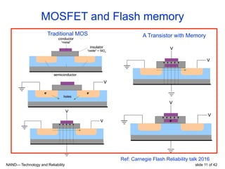
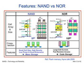
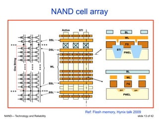
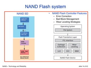
1. NAND Flash
– Technology and Reliability Issues
Swetha Mettala Gilla
Maseeh College of Engineering and Computer Science
Portland State University
Summer 2017
slide 1 of 63
2. NAND— Technology and Reliability slide 2 of 42
§ Introduction
q Memories
q Flash Applications
§ Flash Memory Technology
q NAND Flash
q Flash MCL
q Flash Operations
§ NAND Flash Reliability (Planar)
q Endurance (sustain stress and trap-up)
q Data retention (intrinsic)
q Program interference
All the content is from Internet search
Outline
3. NAND— Technology and Reliability slide 3 of 42
References
[1] Chimenton et al., “Improving Performance and Reliability of NOR-Flash
arrays by using Pulsed Operation,” Microelectronics Reliability, Jul 2006.
[2] Micheloni et al., “Ch5. Error Correction Codes for Non-volatile Memories”,
Springer International publications, 2008.
[3] Hynix, “Flash Memory Technology”, Hynix Semiconductors Micron Tech Slides,
2009.
[4] Khiwan Choi, “NAND Flash Memory”, Samsung electronics Slides, 2010.
[5] Chimenton et al., “A Statistical Model of Erratic Behaviors in Flash Memory
Arrays,” IEEE Transactions on Electron devices, Nov 2011.
[6] Zambelli et al., “Nonvolatile Memory Partitioning Scheme for Technology-
Based Performance-Reliability Tradeoff,” IEEE Embedded Systems Letters,
March 2011.
[7] Meza et al., “A Large-Scale Study of Flash Memory Failures in the Field”,
SIGMETRICS, 2015.
[8] Onur Mutlu, “Reliability (and Security) Issues of DRAM and NAND Flash
Scaling”, Memory Reliability Workshop slides, Carnegie Mellon, 2016.
[9] Spinelli et al., “Reliability of NAND Flash Memories: Planar Cells and Emerging
Issues in 3D Devices”, IEEE Transactions on Computers, 2017.
4. NAND— Technology and Reliability slide 4 of 42
Memory background
Ref: Carnegie workshop slides 2016
• Non-Volatile Memories
– A non-volatile memory is a memory that can hold its information without
the need for an external voltage supply. The data can be electrically
cleared and written.
• Limits of charge memory
– Difficult charge placement and control.
• Flash: floating gate charge
• DRAM: capacitor charge, transistor leakage
– Reliable sensing, data retention and charge control become more difficult
as charge storage unit size reduces.
5. NAND— Technology and Reliability slide 5 of 42
Memory technology
Ref: Hynix slides 2009
6. NAND— Technology and Reliability slide 6 of 42
Memory performance
Ref: Hynix slides 2009
10. NAND— Technology and Reliability slide 10 of 42
Evolution of NAND flash memory
• Flash memory applications
• Portable devices, laptop PCs, and enterprise servers
Ref: Carnegie Flash Reliability talk 2016
11. NAND— Technology and Reliability slide 11 of 42
MOSFET and Flash memory
Ref: Carnegie Flash Reliability talk 2016
Traditional MOS A Transistor with Memory
12. NAND— Technology and Reliability slide 12 of 42
Features: NAND vs NOR
Ref: Flash memory, Hynix talk 2009
13. NAND— Technology and Reliability slide 13 of 42
NAND cell array
Ref: Flash memory, Hynix talk 2009
14. NAND— Technology and Reliability slide 14 of 42
NAND Flash system
NAND SD • NAND Flash Controller Features
– Error Correction
– Bad Block Management
– Wear Leveling Strategies
15. NAND— Technology and Reliability slide 15 of 42
Flash cell operation read
Ref: Flash memory, Hynix talk 2009
16. NAND— Technology and Reliability slide 16 of 42
Flash write methods
Ref: Carnegie Flash Reliability talk 2016
17. NAND— Technology and Reliability slide 17 of 42
NAND flash: program & erase
Ref: Flash memory, Hynix talk 2009
18. NAND— Technology and Reliability slide 18 of 42
Flash cell coupling ratio
Ref: Flash memory, Hynix talk 2009
• Coupling ratio
1. For fast programming, high Vfg is required
2. Either high Vcg or large Alpha cg.
19. NAND— Technology and Reliability slide 19 of 42
Increasing Flash Density (MLC)
Ref: Carnegie Flash Reliability talk 2016
• Multilevel Cell (MLC)
1. Has several threshold voltages
2. MLC requires 2 reads
20. NAND— Technology and Reliability slide 20 of 42
Multilevel Cell Flash
Ref: Flash memory, Hynix talk 2009
• Multilevel Cell (MLC)
– 2 bits and 3 levels
• Storing data in SLC, MLC and
TLC NAND
26. NAND— Technology and Reliability slide 26 of 42
Flash reliability
Retention
• Ability to retain valid data for a prolonged period of time (non-volatile)
• Charge loss due to: de-trapping of electrons/holes
• Oxide defects
• Mobile ions
• Contamination
• Stress-induced leakage current
• Data retention prohibits tunnel oxide scaling
Endurance
• Ability to perform even after a large number of program erase cycles
• Causes: high electric fields inside the cell and high currents
• Wear out occurs: conductors become less conductive, dielectrics become less isolating
• One cell is programmed but entire row endures drain stress.
27. NAND— Technology and Reliability slide 27 of 42
How Flash Fails
• Bit flips
• Access limitations
• Program/erase cycles
• Retention
• Read/program disturb
28. NAND— Technology and Reliability slide 28 of 42
Bit flips
• Some cells don’t reach Vref
• Some cells are not fully erased
• Worse for MLC
• Work-around
Error Correcting Codes (ECC)
• ECC can detect or correct N
bitflips
29. NAND— Technology and Reliability slide 29 of 42
Error Correcting Codes
• Hamming
• Correct 1 bit, detect 2 bit
• 2*n parity bits protect 2n data bits
• Bose, Ray choudhuri, Hocquenghem (BCH)
• Correct M bits over 2n data bits with n*M parity bits
• Low density parity code
• Hamming but more freedom of # parity bits
• Can use soft information
• Working with ECC
• Extra area in Flash to store ECC
• When writing, also write ECC
• When reading calculate ECC and compare
• Correction algorithm if ECC is wrong
• Calculating ECC requies entire page
30. NAND— Technology and Reliability slide 30 of 42
Access limitations
• Erase blocks
• Erase full eraseblock before writing
• Write once
• ECC
• Read and write full sub-pages (512
bytes)
• MLC
• Write full pages
• Write upper page then lower page
• Flash file system
• Only write to erased pages
• Collect writes until a page is filled
• Copy on write file system
• Journal to deal with power failure
• Erased pages (empty space)
require special handling
• Each page can be written only
once
• ECC of erased page will be
wrong
• Software must detect this and
return 0XFF page
• Flashing tools should not
write all 0x FF pages
31. NAND— Technology and Reliability slide 31 of 42
Program/erase cycles
• Some electrons captured in dielectric
• Don’t escape easily even during erase
• Changes Vt
32. NAND— Technology and Reliability slide 32 of 42
Flash error analysis: P/E cycles
• Raw bit error rate increases exponentially with P/E cycles
• Retention errors are dominant
• Retention errors increase with retention time requirement.
33. NAND— Technology and Reliability slide 33 of 42
Manage/store bad blocks
Manage bad blocks
• When #errors is too high, mark
block as bad
• Flash chip detects failed erase
• Flash chip detects write errors
• Detect when #corrected errors
is high
• Torture erase block to confirm
– erase, check 0xff, write pattern,
check pattern
• ⇒ Scrubbing
• Some blocks already marked
bad in factory
Store bad blocks
• Two bytes in OOB of 1st page
– 0xFF 0xFF ⇒ OK anything else ⇒ BAD
– Consumes 2 OOB bytes → less space for
ECC BCH4 / 512 bytes = 8 bytes → 64
bytes / 2KB
– Used by factory-marked bad blocks
• Bad block table at well-known
flash location
– Must have enough space, if BBT itself goes
bad
– Must have 2 copies to deal with power
failure
Limit P/E cycles
= wear leveling
• Keep track of # erase
• Don’t write to same location
• Write to block with lowest erase
34. NAND— Technology and Reliability slide 34 of 42
Retention
• Electrons leak after some time
• Floating gate surrounded by insulator
• But still not perfect
• Retention is strongly dependent on temperature
35. NAND— Technology and Reliability slide 35 of 42
Retention error mechanism
• Retention error: due to electron loss from the floating gate
• Cells with more programmed electrons suffer more from retention errors
• Threshold voltage is more likely to shift by one window than by multiple
36. NAND— Technology and Reliability slide 36 of 42
Retention error value dependency
• Retention error dependent on value
• Cells with more programmed electrons tend to suffer more from retention
noise (i.e. 00 and 01)
38. NAND— Technology and Reliability slide 38 of 42
NAND program inhibit
Ref: Flash memory, Hynix talk 2009
• Programming inhibit
– Red cells should not be programmed (inhibit)
– The higher Vpass, the better Vpgm
disturbance
– But, higher Vpgm cause Vpass disturbance
• Cells
– Pages on same bitline
– Pages on same wordline
– Upper pages in same cell
• More important than read disturb
• 1->0 more likely effected
39. NAND— Technology and Reliability slide 39 of 42
NAND read disturbance
Ref: Flash memory, Hynix talk 2009
• Reading disturbance
1. Increasing Vread -> soft program occur in the unselected cell
of selected string
40. NAND— Technology and Reliability slide 40 of 42
NAND cell interference
Ref: Flash memory, Hynix talk 2009
• Cell interference
– Unwanted Vt shift by the P/E status of adjacent cells
41. NAND— Technology and Reliability slide 41 of 42
How to deal with disturb
• Detect bit flips and mark blocks for refresh
• Make sure that all pages are regularly read
• Also good for retention
(as long as device stays on)
• program disturb solutions: couldn’t find resources
43. slide 43 of 42NAND— Technology and Reliability
Back up
44. NAND— Technology and Reliability slide 44 of 42
Flash reliability
Flash reliability concerns
• Regular concerns of CMOS
• Oxide breakdown
• Interconnect problems (EM)
• Specific to Flash
• Retention
• Endurance
Scaling
• Make flash cell more compact?
• Dominant problem: scaling the dielectrics
Specific to Flash
• Fast programming and erasing done by controlled tunneling
• Leads to oxide degradation (trapping)
Functional requirement
• No charge leakage in stand by situation
• Distinguish 0 and 1 even after intensive use.
Ref: Cell-aware, White paper MentorG 2011
45. NAND— Technology and Reliability slide 45 of 42
Testing Methodology
Erase errors
• Count the number of cells that fail to be erased to ‘11’ state
Program interference errors
• Compare the data immediately after page programming and data after the
whole block programmed
Read errors
• Continuously read a given block and compare the data between
consecutive read sequences.
Retention errors
• Compare the data read before retention and after retention
• Characterize short term retention errors under room temperature
• Characterize long term retention errors by baking in the over under 125
degree C
46. NAND— Technology and Reliability slide 46 of 42
Flash cell
• MOS transistor + floating gate
• Vth changed -> store data
47. NAND— Technology and Reliability slide 47 of 42
NAND operation: write
• Write operation (part1)
• Incremental Step Pulse Programming plus verify scheme
48. NAND— Technology and Reliability slide 48 of 42
NAND operation: write
• Write sequence (part2)
• Shift data in shift registers
• Issue command to program data into page
49. NAND— Technology and Reliability slide 49 of 42
NAND device operation
• Interleave access
• Data bandwidth
• Data transfer time + page access time