SlideShare a Scribd company logo
1 of 91
Download to read offline
UNCLASSIFIED 9i~~'
SECURITY CLASSIFICATION OF THIS PAGE (When DaaeEntered),____________________ h
REPORT DOCUMENTATION PAGE BEFR COSTPLETINSOR
I. RPOR NUM3ER2. GOVT ACCESSION HO. 3. RECIPIENT'S CATALOG NUMBER
4. TITLE (and Subtitle) S. TYPE OF REPORT 6 PERIOD COVERED
A, 1(A--BND iP
,LUPY 09 AKILTURZE- MS THESIS
CCU?LEO CAV 9- b CKVD ,5LOT S. PERFORMIVIG ORG. REPORT NUMBER
7. AUTHOR(.) 5. CONT RACT OR GRANT NUMBER(.)
03Ef
.H CMAr-H
-. t3'JPNkS
9PERFORMING ORGANIZATION NAME AND ADDRESS 10. PROGRAM ELEMENT.' PROJECT. TASK
AREA & WORK UNIT NUMBERS
AFIT STUDENT AT: LUoi vus iTy O :ILL) 001-
CONTROLLING OFFICE NAME AND ADDRESS t2. REPORT DATE
1988
13. NUMBER OF PAGES
MONITO'NING AGENCY NAME 81 ADDRESS(If different from Controlling Office) IS. SECURITY CLASS. (of this. rePort)
AFIT/NR UCASFE
SWright-Patterson AFB OH 45433-6583 UNa
DCLASSFIEIODONRDG
SCNHEDULE
~I DISTRIBUTION STATEMENT (of this Reporl)
< DISTRIBUTED UNLIMITED: APPROVED FOR PUBLIC RELEASE
17. DISTRIBUTION STATEMENT (of the
abs tracfente red o
in lnc 20, If different from Repor t AUG 0 4 988
SAME AS REPORT
1SUPPL-EMENTARY NOTES LYNNve
E. r
WOLAVERlease:j) IAW AFR 190-1
Dean for Research an4'Prote-ssional Develomn
Air Force Institute f Technolog
Wright-Pattcerso AFBOH 45433-6S83
19. KEY WORDS (Continue on reverse side If necessary ttd Identify by block number)
20. ASSTRACT (Conntinue on reverse side It necensary and Identify by block number)
ATTACHED
DID I O F 1413 EDITION OF I NOV 65 IS OBSOLETE JtCLJjjUE
SECURITY CLASSIFICATION OF TNIS PAGE (When Date Entered)
ABS TRACT
A Broad-Band Array of Aperture-Coupled Cavity-Backed Slot Elements
A broad-band array of aperture-coupled cavity-backed slot (CBS) elements was
designed, constructed and tested. The antenna array design incorporated two
major departures from previous CBS arrays: aperture coupling, and 'half-width'
cavities. Expiremental results demonstrated these departures enhance the po-
tential for larger operating bandwidths using less physical space than pre-
vious arrays of CBS elements. Computer simulation and test results also in-
dicated that the antenna array was not hindered by the presence of a large
structural stopband such as was observed in all previous CBS arrays. Con-
sequently, modulation of the antenna feedline impedance was not required for
satisfactory performance. Antenna patterns for the array were similar over the
frequency range 1.75 - 3.5 GHz.
ceessicn For
DC sT.ki E
AvailabilJity i '4
U
A,9 "an2lor
ua.'st $
iproclal
A BROAD-BAND ARRAY OF
APERTURE-COUPLED CAVITY-BACKED
SLOT ELEMENTS
BY
JOSEPH MICHAEL BURNS
B.E.E., AUBURN UNIVERSITY, 1981
THESIS
Submitted in partial fulfillment of the requirements
for the degree of Master of Science in Electrical Engineering
in the Graduate College of the
University of Illinois at Urbana-Champaign, 1987
Urbana, Illinois
iii
ACKNOWLEDGEMENTS
There are many besides the author who made this paper possible. The
author wishes to thank his advisor, Professor Paul E. Mayes, for his superb
guidance, patience, and prodding. He would also like to express his appre-
ciation to Jeff Kromer for expertly building the antennas discussed herein;
Jim Drewniak for his training in antenna design, construction and testing;
Hugh Smith, Tom Sons, and Dave Tammen for sacrificing countless hours in an
effort to obtain antenna patterns for this report; and all the other people
in the Electromagnetics and Electromagnetic Communication Laboratories who
helped with this research over the last year.
In addition, the author would like to thank his office mates, Captain
Charles F. Smith and Captain Mark A. Mehalic, for their assistance with the
computer programs in the appendices of this report. Others whose help
contributed to this research include the Air Force Institute of Technology,
who paid the author's tuition and fees; TRW, Incorporated, who provided
funding (a portion of which went directly to this work) for research on
slot antennas; and Professor Weng C. Chew, whose enthusiastic, enlightening
and patient teaching of an early electromagnetics course sparked the
author's interest in this subject.
Of course, the author wishes to express loving thanks to his wife
Cindy, and their children Melissa, Amanda, Daniel, and Timothy for their
support, understanding, prayers, and love. Finally, and most importantly,
the author wishes to thank Almighty God for demonstrating many times
during this work that 'I can do a1 rhin-- tbrnc:gh Christ who gives me
strength.'
iv
TABLE OF CONTENTS
CHAPTER Page
1. INTRODUCTION .......... ......................... . 1
2. ANTENNA DESIGN AND CONSTRUCTION ....... ............... 3
2.1 Szmurlo's Antenna .......... .................... 3
2.2 Cavity Design ........... ...................... 5
2.3 Cavity Construction ....... ................... . 11
2.4 Aperture Coupling ....... .................... . 11
3. PROTOTYPE I .......... ......................... . 14
3.1 Prototype 1 Construction ...... ................ 14
3.2 Prototype 1 Testing Procedure ..... .............. 15
3.3 Advantages of Aperture Coupling .... ............. . 16
3.4 Prototype I Data and Analysis ..... .............. 17
3.5 Conclusions from Prototype I Testing ... .......... 25
4. OTHER PROTOTYPES .......... ...................... 26
4.1 The High Frequency Anomaly ..... ............... 27
4.1.1 Determining the cause ..... .............. 28
4.2 Further Testing of Prototypes 2, 3, and 4 .. ........ . 35
5. LOG-PERIODIC ARRAY OF APERTURE-COUPLED CAVITY-BACKED SLOTS . . 36
5.1 Feed Network/Cavity Bottom Design and Construction . . 36
5.2 S Parameter Measurement ...... ................. . 40
5.3 Antenna Array Pattern Measurements ... ........... . 43
6. COMPUTER SIMULATION AND STOPBAND ANALYSIS ... ........... 49
6.1 The Shorted-Stub Model of a Single Cavity .. ........ . 49
6.2 Location of the Structural Stopband ... ........... . 52
6.3 Eliminating the Structural Stopband ... ........... . 55
6.4 Effect of Eliminating the Structural Stopband
on Antenna Impedance ...... .................. 56
6.5 Cause and Impact of the Narrow Stopband ............. 9
7. CONCLUSIONS AND RECOMMENDATIONS ...... .............. 62
V
APPENDICES ........... .......................... 64
A: COMPUTER PROGRAM TO CALCULATE S PARAMETERS
OF SHORTED STUB MODEL ....... .................. 64
B: COMPUTER PROGRAM TO LOCATE THE STRUCTURAL STOPBAND . . . . 66
C: COMPUTER PROGRAM TO DETERMINE THE IMPEDANCE OF
THE MODULATED LINE ........ .................... 69
D: COMPUTER PROGRAM TO CALCULATE THE S PARAMETERS
OF A LPCBS ARRAY ........ ..................... 72
E: COMPLETE ELEVATION PATTERNS OF 11 CAVITY ANTENNA ARRAY
BY FREQUENCY AS MEASURED IN ANECHOIC CHAMBER ........ .. 76
REFERENCES ........... .......................... 81
vi
LIST OF TABLES
Table Page
3.1 PROTOTYPE 1 - PARAMETERS OF INTEREST .... ............ 19
3.2 POWER DISTRIBUTION AMONG ARRAY ELEMENTS, T 0.92
COUPLING SLOT LENGTH - 4.5 cm ...... ................ 24
vii
LIST OF FIGURES
Figure Page
1. Szmurlo's antenna [51 ..... .. .................... 4
2. Closed cavity, d << X .......... .................... 5
3. Top view of cavity with H wall ........ ................ 7
4. Top view of modified cavity ........ ................. 7
5. Modified cavity with slot ......... .................. 8
6. Exploded view of completed antenna ..... ................. 12
7. Aperture coupled cavity-backed slot antenna .. ......... ... 13
8. (a) S11 - Szmurlo's cavity 6 [51 ..... ............... ... 17
(b) S11 - Prototype 1, coupling slot length = 11.45 cm . . .. 17
9. S1I and S2 1 - Prototype 1, coupling slot length: 4.5 cm,
coupling slot position: against cavity wall opposite
radiating slot .......... ........................... 18
10. Efficiency versus frequency; coupling slot length = 4.5 cm . . 21
11. Antenna array with T - 0.92. To determine size of smaller
cavities, multiply dimensions of right-most cavity by (0.92)m. 23
12. (a) S11 - Prototype 2. (10.6 - 11.4 GHz) ... .............. 27
(b) S21 - Prototype 2. (10.6 - 11.4 GHz) .... ..........
... 27
13. Sii - Prototype 2 with plexiglass clamps. (10.6 - 11.4 GHz).. 28
14. S1 1 - Prototype 2 with shallower slot. (10.6 - 11.4 GHz) . . 29
15. S11 - Prototype 3. (6.5 - 8.5 GHz) .... ............. ... 29
16. S11 - Prototype 3 with 15 mil thick microstrip feed.
(6.8 - 8 GHz) .......... ........................... 30
17. (a) TDR - Poorly matched line ...... ................ .. 31
(b) Return loss - Poorly matched line .... ............ . 31
18. Return loss - Through ........ .................... . 32
19. (a) TDR - Reference short ....... ................. ... 33
(b) Return loss - Reference short ..... ............. ... 33
20. (a) S1I - Prototype 3 ........ .................... . 34
(b) Return loss - Reference short ..... .............. . 34
viii
Figure Page
21. Section of meandering line between two coupling slots . ... 38
22. Eleven cavity array feedline ...... ................. . 41
23. Measured SlI - 11 cavity array ..... ............... 42
24. Measured S2 1 - 11 cavity array ..... ............... 42
25. SIl - Szmurlo's 6 cavity array with
unmodulated feed. (Frequencies in MHz) ... ........... . 42
26. Azimuthal patterns for 11 cavity array .... ............ . 44
27. Elevation patterns for 11 cavity array .... ............ . 46
28. Shorted-stub model of cavity [5] ...... ............... 49
29. (a) Computed S11 using cavity model .... ............. 50
(b) Measured S1j - Prototype 1. (0.75 - 2.25 GHz).........
... 50
30. Model of cavity being fed by a modulated microstrip feed [5] . 51
31. jZif versus f (GHz) - Element 7 with unmodulated feedline 53
32. Phase versus f (GHz) - Element 7 with unmodulated feedline 54
33. Phase versus f (MHz) - Szmurlo's cavity 6 .. .......... . 55
34. JZij versus f (GHz) - Element 7 with modulated feedline . . 57
35. Phase versus f (GHz) - Element 7 with modulated feedline . . . 57
36. Computed S11 - 11 cavity array with unmodulated
feedline. (1.0 to 4.5 GHz) ...... .................. . 58
37. Computed S
11 - 11 cavity array with modulated
feedline. (1.0 to 4.5 GHz) ...... .................. . 59
CHAPTER 1
INTRODUCTION
In recent years, there has been a burgeoning interest in low-profile,
wide-band antennas. Low-profile antennas have numerous applications, espe-
cially for missiles and aircraft, because only these antennas can be con-
formally mounted. The most popular types of thin antennas are the microstrip
patch and the cavity-backed slot (CBS). Much research has been done on
both types, but the project reported herein involves only CBS antennas.
The main objective of this research is to extend the operating bandwidth of
a log-periodic (LP) array of thin CBS elements.
Research on CBS antennas dates back more than thirty years. Mayes
provides a good summary of early research and recent progress in developing
low-profile, wide-band CBS antennas in his report Very Wide Band Antennas
for Missile Fuze Applications [1]. One problem encountered in early
attempts to design log-periodic arrays of CBS elements was the structural
stopband which occurs in a periodic array of such elements. In this band
of frequencies there is no propagation down the feedline. When a corre-
aponding region of attenuation occurs between the feedpoint and the active
region of a log-periodic cavity-backed slot (LPCBS) array, the wave
launched at the input is mostly reflected before it reaches the active
(radiating) region. The structural stopband is caused by additive reflec-
tions from discontinuities presented by the slots. Ingerson and Mayes [2]
found that modulating the feedline impedance was an effective way of elimi-
nating the stopband. Building on their work, Ostertag [3] designed an
LPCBS array using smaller cavity depths and obtained a 50 9 mean impedance
through use of a computer-synthesized modulated impedance feedline. More
2
recently Tammen's research [41 focused on eliminating the structural stop-
bands associated with many LP antennas by combining CBS and monopole ele-
ments. Finally, Szmurlo [5] concentrated on increasing the bandwidth of an
LPCBS array while using very thin cavities of constant depth and optimizing
the design of the modulated impedance feedline. The bandwidth achievable
by antennas of his design is limited because of the immense amount of space
they require.
The goals of this research were to design and build an LPCBS antenna
which has a larger operating bandwidth, uses less 'real estate', and oper-
ates at much higher frequencies with a larger power gain than previous
LPCBS arrays. Achieving these goals requires taking several large steps
forward from the work done by Szmurlo. First, in an effort to reduce
losses, the antenna was designed to have air-filled cavities rather than
Rexolite-filled ones. Second, the cavities were to be excited by aperture
coupling, that is, energy would be coupled into the cavity through an aper-
ture in the bottom of the cavity rather than through the radiating slot in
the top of the cavity. Third, a new theory would be applied that allowed
each elemental cavity to be built only half as wide as Szmurlo's elemental
cavities. This theory and application will be discussed in more detail in
Chapter 2. Finally, it was desired that this new antenna would operate at
higher frequencies than any previous LPCBS. The high frequency testing of
the new antenna led to previously unseen problems, as will be pointed out
in Chapter 4.
3
CHAPTER 2
ANTENNA DESIGN AND CONSTRUCTION
Before constructing an LP array of CBS antennas that introduced
several new departures from the previous case, it was considered prudent to
test several prototype elements. From the testing of these prototypes, the
scaling factor (T) and many other useful design criteria used in the LP
array were determined.
This chapter will focus on the design and construction of these proto-
types. The testing of these prototypes and the selection of design cri-
teria will be discussed in detail in Chapters 3 and 4.
2.1 Szmurlo's Antenna
Since this research was, in many ways, a continuation of Szmurlo's, it
is useful to have a more detailed understanding of his antenna. A descrip-
tion from his thesis follows.
The antenna was constructed from a I/P-inch sheet of
Rexolite 2200. An aluminum sheet (also 1/8 inch) was used
a, backing for the Rexolite to provide support and to pro-
vide threaded holes for the screws. The brass screws that
form the vertical cavity walls were approximately 1/2 inch
apart for the four largest cavities and about 3/8 inch apart
for the remainder. These spacings had been determined ade-
quate to make the S-parameters of an isolated cavity-backed
slot with screw walls agree very well with those of one with
solid walls. Copper cladding forms the top and bottom
walls. A slot was cut into the top cavity wall by removing
the copper cladding to allow the cavity to radiate when
excited. A drawing of the cavities formed on the Rexolite
is shown in Figure 1.
To excite the cavities, a microstrip feed is passed over the
slot of each cavity. It was found that for symmetrical pat-
terns, the slot should be fed from the center. The feedline
was constructed on a 1/16-inch sheet of Rexolite 2200. The
characteristic impedance of the feedline was trimmed to 50 ohm
CY4
+
- -S
I.s
~h~tMIS
5
by observing its response when tested with a TDR. After
using the TDR, Lhe copper ground plane of the feed was cut
away where it would lay over the cavity slot. Good contact
between the ground plane and the cavity top wall must be
maintained, particularly in the vicinity of the slot, or
antenna performance will degrade.
A type N female bulkhead connector is present at both ends
of the feed. This allows for the measurement of reflection
and transmission coefficients of the antenna [5].
The antenna built by Szmurlo operated from 975 to 1325 MHz.
2.2 Cavity Design
As mentioned previously, the antenna was designed utilizing a theory
that allowed each elemental cavity to be built half as wide as elemental
cavities in previous CBS antennas. This theory was first proposed by
Tanner [6]. The basis for the bisection of the cavity can be seen by first
analyzing a closed cavity which is very thin (as compared to a wavelength)
in the z direction as shown in Figure 2.
Z
d0
Fub y
.x
~Figure 2. Closed cavity, d <( A.
6
For the transverse magnetic (TM) case, the time-harmonic (ej
wt
timp
dependence suppressed) fields inside this cavity can be written as:
E - E sin mx sin nly [7] (2.1)
z mnp a b
-j mnp I
i n)
Eo (ncos (71 (2.2)
(mlr)2 m 2 sin -a (S
jwe E mr Cos mrx) sin [71
y (mw)2 nn 2 aa bo [(3
where the z dependence has been dropped because of the thinness in the
z direction. Substituting the equation for Ez into the Helmholtz equation,
(V2 + B2) E - 0, yields the dispersion relation
2 O (mx)2 + (2.4)
Solving this equation for w yields
1 mst 2 +n 2 1/2
w nm)
/ - a (2.4a)
which is the resonant frequency of the mn mode of this cavity. One can
also note from the field equation E (with m - n = 1) that as x is held
z
constant and y is varied, E reaches a maximum at y - b/2. Furthermore, at
z
y - b/2, Hx - 0 for the TM110 mode. Thus, an H wall (a surface along which
HRTAr
- 0) can be inserted in the plane (x, b/2, z) without interfering with
the fields of the cavity. (Note: in most previous rectangular CBS anten-
nas, the radiating slot was placed along the line (x, b/2, d)). A top view
of this cavity with the H wall inserted would look like Figure 3.
7
X
4--H Wall
-- E Wall
zI
b/2 Y
Figure 3. Top view of cavity with H wall.
Next, consider a cavity that has a top view much like half of the
cavity in Figure 3. Pictorially, a top view of this cavity would look like
Figure 4 below.
x
1-H Wall
E Wall
Z b/2 y
Figure 4. Top view of modified cavity.
8
One three-dimensional realization of this cavity is shown in Figure 5.
Z
x - - hls
-Slot in Cavity Top
b/2 Y
X
Figure 5. Modified cavity with slot.
To determine the field equations of this modified cavity, begin with the
phasor form of Maxwell's equation
- V z
Z Ez J wu0H (2.5)
or, using rectangular coordinates and writing the curl as a determinant
yields
ax ay az i" 0 H (2.6)
o 0 E
z
aEZ aE +
ay a " 0 H (2.7)
zE aE
Therefore --- 3-
( E-z x 28Z)
J1 ax a (2.8)
L0
9
To find E , use the Helmholtz equation.
zz
[V2
+ w2 o0co0]
Ez .0(2.9)
This equation admits solutions of the form
0 sin x f sin Byy (
cos
E
o [8] (2.10)
Cos 0yy Cos Byy
where only one solution in each of the brackets must be selected. (Note
also that the variation with z has again been dropped because of the thin-
ness of the cavity in the z direction.) To determine which solutions to
select, consider the boundary conditions
EZ (x, 0, 0) --0 (2.11)
Z
E (0, y, 0) = 0 (2.12)
a
EZ (-a, y, 0) = 0 (2.13)
H (x, b/2, d) - 0 (2.14)
x
It is apparent from the first two boundary conditions that the only
admissible solution for E is
Ez - E sin $ x sin 8yy (2.15)
From the third boundary condition, it is clear that sin 8x (-a) = 0 or
=--- IF
Bx (2.16)
Now, the magnetic field can be calculated from (2.8)
-8y
H " (E° sin (SxX) cos (6yY)] (2.17)
Hx jW 0 0 x
o
The fourth boundary condition states that Hx (x, b/2, d) = 0. Therefore,
mm m fmmmmmmmm~
- -- "
10
8 b/2 n-
nodd
or Sy. (nZ); n odd (2.18)
Substituting (2.16) and (2.18) into (2.15) yields
E = E sin ( ) sin (.) (2.19)
2
Substituting (2.19) into (2.9) and solving for W ioCo0 give
2 (37r2 niT)2
(2.20)
o , +
which is the dispersion relation for the modified cavity. Solving (2.20)
for w yields
= n I [m(RI) 2 + (n T2]1/2 2.21)
mn - aI- ''J](.1
/ Uo Eo
which is the resonant frequency for the mn mode of this modified cavity.
Rewriting some of the important equations for the modified cavity:
Em E sin (--)
sin (fly) (2.22)
H- /b [E sin (") cos (2.23)
1 mir2 nn 2 1
/2
W 1 [ (-) + (a-)] (2.24)
Mn O a b
Note that these three equations for the modified cavity are of the same
form as (2.1), (2.2) and (2.4a) for the closed cavity of Figure 2. In
fact, (2.24) and (2.4a) are exactly alike. Thus, a cavity can be created
that is one half as wide as the closed cavity of Figure 2 (and still have
11
the same resonant frequency) by extending a slat across the top of the
cavity as shown in Figure 5. This is an extremely encouraging result
because it means that an array of modified cavity antennas (of the type in
Figure 5) can be built in about half the space of the previous arrays which
used unmodified cavities (of the type in Figures 1 and 3). The antennas
tested during this research were all designed in accordance with Figure 5
for a specific resonant frequency as given by (2.24).
2.3 Cavity Construction
In general, the prototype cavities were constructed by milling
1/16" deep into a 1/8" brass sheet. The length and width of the cavities
were determined by Eq. (2.24) with m = n - I since we are interested in
using the TMI1 0 mode. The radiating slot was cut along the length of one
edge of the cavity. At this point, the sides, top and radiating slot (in
the top of the cavity) were completed. The bottom of the cavity was a
sheet of double clad 1/16" Rexolite (E = 2.6) fastened to the cavity body
r
by brass screws tapped into the 1/8" brass. Figure 6 illustrates an
exploded view of the completed antenna.
2.4 Aperture Coupling
To turn this slotted cavity into an antenna, energy must somehow enter
into the cavity and be radiated out the radiating slot in the top. In the
past, this was usually done by either inserting a probe in the bottom of
the cavity, or running a microstrip line across the radiating slot as
Szmurlo did (see Chapter 1). Instead of using one of these traditional
12
,,..
z e. -. 14%
S101

0
0
0
0
ln¢o
/A
Figure
6. Exploded
view
of completed
antenna.
methods
to feed
these
cavities,
a new approach
was used:
aperture
coupling.
In aperture
coupling,
one side
of the double-clad
Rexolite
is
the cavity
bottom.
On the other
side,
the copper
cladding
is peeled
away
except
for a strip
of a specific
width
(4.4
mm for 50 in 1/16"
Rexolite)
which
acts
as the antenna
feedline.
On the cavity
bottom
side,
a narrow,
short
strip
of copper
orthogonal
to the
feedline
(which
is on the other
side)
is peeled
away
to form
the coupling
aperture
(or coupling
slot).
An
example
of an aperture
coupled
cavity-backed
slot
is shown
in Figure
7.
Aperture
coupling
has some
advantages
over
the more
traditional
methods
of
feeding
the cavity.
For one thing,
it is a flatter
system
of feeding
the
antenna
than
probe
feeding
and thus
is better
suited
for conformal
mounting.
Additionally,
aperture
coupling
does
not interfere
with
the
radiation
of energy
through
the radiating
slot.
When
the same
slot
is
used
for both
coupling
and radiation,
this
interference
(scattering
from
13
Radiating Slot
Copper Cavity Coupling Aperture (Slot)
Ground Plane
(Bottom) - ------
Feed Line
i. Rexollte (E?:2.6)
1/16"
Figure 7. Aperture coupled cavity-backed slot antenna.
the feedline) is unavoidable. With aperture coupling, the feedline can be
placed anywhere along the slot (not just the center) without affecting the
antenna patterns. Finally, aperture coupling offers a new degree of
freedom, variation of the coupling aperture size, not available heretofore.
On the other hand, when aperture coupling is used, some radiation will leak
out the coupling aperture. Thus, power gain may be lower when aperture
coupling is used.
Aperture coupled antennas are relatively new devices. Pozar [9] first
proposed the concept for exciting microstrip patch antennas in 1985. Since
then he and others, notably Sullivan and Schaubert [1I, have investigated,
with some success, the use of aperture coupling with simple microstrip
patch antennas. However, until now, aperture coupling has not been used to
drive cavity-backed slot antennas.
14
CHAPTER 3
PROTOTYPE 1
In this chapter, the first prototype antenna and initial testing will
be discussed. Four prototypes were constructed and tested: one that was
the same size as the largest cavity in the array (Prototype 1), one the
same size as the smallest cavity in the array (Prototype 2) and two others
in between the largest and smallest cavities (Prototypes 3 and 4). The
testing on Prototype 1 was by far the most conclusive. The results of
various tests on this prototype were used to establish the length and posi-
tion on the cavity bottom of the coupling slot as well as the antenna array
scaling factor (T). Testing on Prototypes 2 and 3 had some unexpected
results, which will be discussed in the next chapter.
3.1 Prototype 1 Construction
Prototype I was built to the specifications of Figure 5 with a = 10
9/16" (26.829 cm), b/2 1
1 17/32" (3.889 cm), and W . 5/32" (0.3969 cm).
5
The cavity bottom/feedline was constructed of 1/16" Rexolite (e = 2.6).
r
On the feedline side, all the copper except a narrow strip (the feedline)
was removed. The width of the strip (4.4 mm) was determined by formulas
proposed by Edwards [11] for the given height (1/16") and a characteristic
impedance of 50 ohms. SMA connectors were attached to each end of the
line. The line was tested on a TDR and trimmed for a good match. The
coupling aperture was then cut in the middle of the other side of the
Rexolite with the arbitrarily selected width of 2.5 mm and length 11.45 cm.
The length of the coupling slot was easily varied by covering portions of
the 11.45 cm opening with copper tape. The position of the coupling slot
15
in the cavity bottom was also variable by simply loosening the connecting
screws and sliding the cavity bottom in either direction.
To determine the resonant frequency of this cavity, its dimensions
were substituted into Equation (2.24). This substitution resulted in a
resonant frequency of 12.615 x 10⁹ rad/s or 2 GHz. For a closed cavity of
these dimensions, a resonant frequency of 2 GHz would be expected. But, in
fact, (2.24) assumes that W - 0 (which it is not) and does not take into
S
account the coupling aperture. Therefore, it was expected that the actual
resonant frequency of Prototype I would be proportionally less than 2 GHz
with the increase in size of the apertures.
3.2 Prototype 1 Testing Procedure
To test Prototype 1, and the other prototypes as well, the following
sequence of steps was followed using the HP 8510 Network Analyzer.
1) Using the calibration kit, a calibration over the frequency range
of interest was executed.
2) The measurement plane was then shifted to coincide with the
coupling aperture. For reflection measurements, this was accomplished
by using a reference short. The short was constructed similar to the
microstrip feed line except it was only half as long and had a shorted
plane on one end. Thus, the electrical distance between the shorted
plane and the connector was equal to the electrical distance between
either connector and the coupling slot of the microstrip feed line.
The short was connected to the HP 8510 and electrical delay and phase
mamlm~ i Imi ( H ( ( m
ms
16
offset were added until the trace (S1) on the 8510 collapsed to a
point at the left edge of the Smith chart on the real axis.
Similarly, electrical delay and phase offset were added to transmis-
sion measurements via a reference 'thru' (which was the cavity bottom/
feed line with the coupling aperture covered with copper tape).
3) Finally, the antenna itself was connected to the 8510 (with the
values of electrical delay and phase offset gained through step 2
above programmed into the 8510) as a two-port device and measurements
recorded of S11 and S21.
3.3 Advantages of Aperture Coupling
Once the first two steps were completed for the cavity bottom/feed
line and cables (from 8510 to antenna), numerous measurements as described
in step three were made with the length and position of the coupling aper-
ture as variables. As expected, the longer the coupling slot, the lower
the resonant frequency (as indicated by a crossing of the real axis by
SI). Furthermore, as the coupling slot was shortened, the size of the
S locus shrunk toward the center of the chart. The impact of this phe-
nomenon can best be seen by comparison of Prototype I data with Szmurlo's
single cavity data. Figure 8a is the S I data for Szmurlo's Cavity 6.
Note the similarity between the shape of the locus in Fig. 8a and that of
Fig. 8b, the S1 data for Prototype i with a coupling slot length of 11.45 cm.
Neither Szmurlo's Cavity 6 nor Prototype 1 (in this configuration) is a
very well-matched radiator (as evidenced by the large distance between the
center of the chart and the crossover point on the real axis at resonance).
17
Figure 8a. Figure 8b
S11 - Szmurlo's cavity 6 [5). S11 - Prototype 1,
coupling slot length 11.45 cm.
Figure 9 shows the S11 and $21 locus for Prototype 1 with the much shorter
coupling slot length of 4.5 cm. Note that the S locus of this figure
indicates a much better match than the antennas of Figure 8. This ability
to affect the antenna impedance by varying the length of the coupling slot
is exciting because it gives the antenna engineer a degree of freedom not
previously available. Conversely, the position 3f the coupling slot had
virtually no effect on the resonant frequency or the shape of the S1 and
S21 loci.
3.4 Prototype 1 Data and Analysis
As stated earlier, the purposes of testing the first prototype
included determining the optimum length of the coupling aperture and the
optimum scaling factor for the log-periodic array. The performance factor
18
MARKER MARKER
1. 77 5 1.7I 5-ki
"-. " "
- .,-.
[__ _
. .. . . . . .--
-. _ -_ ,
START - 6. 00
ThGO@ t START 6. 73e6"6 C43
STOP 2z9966@6 C34Z 51W 2. 2"6000 own
Figure 9. S11 and S2 1 Prototype 1,
coupling slot length: 4.5 cm,
coupling slot position: against
cavity wail opposite radiating slot.
that was used to determine the optimum was the upper bound on the radiation
efficiency as defined by
e , 100 1 - "l 2 _ Is21 2 % (3.1)
Rt I -llol isz
Il 2.I
A close look at this aqcation reveals that the numerator represents the
part of the signal that is neither reflected nor transmitted; this is the
portion of the signal that is radiated (discounting losses). The denomina-
tor, on the other hand, represents the portion of the signal that is not
reflected; this is the sum of the radiated and transmitted portions of the
signal. Hence, (3.1) could be rewritten as
eR 100 radiated (3.2)
relctd hi sth u
Rh radiated n
transmitted otoso h
19
Thus, eR is the percentage of the signal remaining after reflection that is
radiated. It was decided that a radiation efficiency at resonance of
around 60% would be best for application to a log-periodic array. The
reason is that no single element in the array should radiate so much of the
signal that there would not be enough signal left to excite remaining ele-
ments. If e >> 60%, the active region of the array would be made up of
r
just one or two elements.
With this in mind, the data from Prototype I testing were examined to
see how the efficiency changed as a function of the coupling slot length.
As expected, the efficiency declined as the length of the coupling slot
shortened, most likely because less energy is coupled into the cavity as
the coupling slot becomes shorter. The antenna performance with the three
specific coupling slot lengths that yielded an efficiency of around 60% was
then closely scrutinized. Table 3.1 lists the parameters of interest of
these three configurations.
TABLE 3.1
PROTOTYPE I - PARAMETERS OF INTEREST
Coupling Slot Resonant eR M
Length (cm) Freq. (GHz)
5 1.655 72.38
4.5 1.78 53.643
4 1.86875 50.64
20
To determine which of these three coupling slot lengths to choose, and to
simultaneously determine the scaling factor, a power distribution analysis
much like that done by Tammen for his log-periodic array of monopole-slot
elements was performed [4]. The goal of this analysis was to determine how
power would be distributed among the elements of the log periodic array at
different frequencies for a given scaling factor (and in our case, a given
coupling slot length). With this result a scaling factor can be selected
which, for a given frequency, will produce an adequate number of elements
with relative power above a desired threshold. The elements above the
threshold will be those that make up the active region of the antenna for
that frequency.
In a nutshell, the analysis consists of creating an efficiency versus
frequency curve for each cavity in the array. Then, for a given frequency,
the e versus f curve of the smallest cavity can be used to determine what
percentage of power incident on this first cavity will be radiated. Next,
the e versus f curve for the second smallest cavity is used to determine
what percentage of the remaining power is radiated by this second cavity,
and so on. Since it was too difficult to generate an e versus f curve for
each cavity, it was assumed that the curves for all the cavities had the
same shape. To obtain an e versus f curve for the higher frequency cavi-
ties, the frequencies of the e versus f curve for Prototype I were simply
scaled. For individual log-periodic elements, one could expect this
scaling to be accurate. The fact that the cavity depths in our array are
not log-periodically scaled should have little impact. Mayes found that
efficiency versus frequency characteristics for shallow cavities did not
change much with small changes in cavity depth [12].
21
A methodical example will serve to more clearly explain the analysis
described above. For this example a coupling slot length of 4.5 cm and a
scaling factor of T - 0.92 was used. The steps in the analysis follow:
1) Generate an efficiency versus frequency curve for the con-
figuration of interest (e.g., Prototype 1 with a coupling slot
length of 4.5 cm) using iSII I and is211 from the HP 8510 and
Equation (3.1). Figure 10 shows the curve generated for this
example.
70_
60
Resonance
50
0) 40-
30-
20
16
12 1.78
8 1 1 1 1 1 1 I
1
1.3 1.5 1.7 1.9 2.1
f (GHz)
Figure 10. Efficiency versus frequency; coupling slot length = 4.5 cm.
2) Determine the number of cavities, n, in the required array band-
width. Since an electrical bandwidth of 5:1 was desired, it was
felt that a structural bandwidth of 6:1 was needed. To achieve a
6:1 structural bandwidth with T = 0.92 indicates that for any
22
dimension Xo, of the largest element, the smallest element will
m
have that dimension equal to 6 X (0.92) , i.e.,
0
6 X (,. 9 2 ) m
- X
0 0
0.92 m
, 1/6
log (1/6) - 21.489
m log (0.92)
- number of other elements
in addition to the first element. Therefore, 22 elements were
needed to achieve a 5:1 electrical bandwidth with a scaling fac-
tor of 0.92. A drawing of such an array is shown in Figure 11.
3) Generate a power distribution table (see Table 3.2).
a) Translate a particular frequency of interest by multiplying
it by (0.9 2 )m (where m is the exponent referred to in Figure 10).
Start with the highest m in the array and continue to chaage m
until the translated frequency (ft) is greater than or equal to
1.25 GHz, the lowest frequency of Figure 9. (Alternatively,
solve m =
log fre 2 5 GHz
itrest) / log(Q.92) and round up to find
the highest m which yields a translated frequency above or equal
to 1.25 GHz.)
b) From Figure 9, find the value of e corresponding to f and
t
place it in a table (e.g. Table 3.2) where f and m intersect.
c) To find the fractional power for the m-I element, use the
following formula from Tammen [4)
i-I
FPi - e, [100 - I FPn ]
nml
23
' -.
E • ,,.4
.- ,
F. , 0 e'
0 ~ 0
-- -4.
.,o
.~--- -
, ,-4 >i
m.m i i i i
24
- -
I
-o
0 N
ON-
. . . . . , .
-
. . . . . .
N
~'caz --
25
where FPi is the fractional power of the ith element, FP is the
i n
fractional power of the nth element and ei is found from Figure 9
by using ft/.
d) Repeat previous steps until the whole line for the frequency
of interest is filled in (see Table 3.2).
Once the previous steps are completed over a range of frequencies, the
power distribution table can be completed. Several tables for different
scaling factors and different coupling slot lengths were created in this
manner. Based on previous research, it was decided the active region for a
given frequency needed to have at least three elements with relative power
above 10. The table with the greatest bandwidth of frequencies that had
three or more elements with relative power above 10 was selected. That
table corresponded to a r of 0.92 and a coupling slot length of 4.5 cm. It
is reproduced in this report as Table 3.2.
3.5 Conclusions from Prototype I Testing
Many valuable things were learned from testing Prototype 1. First of
all, the data verified the theory of bisecting the traditional rectangular
CBS. Second, the 'optimum' coupling slot length for Prototype 1 was
selected via power distribution analysis. Finally, and most importantly, a
new benefit of using aperture coupling was realized. That is, the perfor-
mance of the prototype antenna (and presumably the performance of the
entire array) can be controlled, in part, by the length of the coupling slot.
26
CHAPTER 4
OTHER PROTOTYPES
It was decided that a second prototype should be built and tested in
order to see if scaling the antenna altered the performance parameters
observed for Prototype I. This second prototype was designed to have the
same dimensions as the smallest element of the antenna array. Based on the
theory of scaling, its resonant frequency was expected to be approximately
11 GHz, an order of magnitude higher than any previously tested CBS
antenna. Since the wavelength shrinks proportionally as the frequency
rises, much greater attention to detail was used when constructing and
testing this higher frequency device than was used when building and
testing Prototype 1. Nevertheless, problems were anticipated and a major
problem was encountered during preliminary testing of Prototype 2.
The basic problem was that the impedance locus of S11 moved in a coun-
terclockwise (instead of clockwise) direction as frequency increased
(Fig. 12a). Interestingly, the $21 locus (Fig. 12b) was normal (clockwise).
When further testing of Prototype 2 did not reveal the cause of the anomaly,
a third prototype with a resonant frequency intermediate to those of
Prototypes I and 2 (fr - 7.35 GHz) was constructed and tested.
Unfortunately, Prototype 3 also manifested the unexplained phenomenon. A
fourth prototype with a resonant frequency still lower than that of
Prototype 3 was constructed and tested (fr . 3.77 GHz); the problem was not
observed for this final prototype. Eventually, the cause of this
frequency-related phenomenon was discovered. This chapter will detail
the problem, the steps taken in search of the cause, the cause, and the
solution to the problem.
27
4.1 The High Frequency Anomaly
Recall from Prototype 1 data (Figure 9) that both the S11 and $21 loci
travel clockwise (CW) around the Smith Chart as frequency increases.
I
11. t
-- - - ,
-- i " " . ,- -, ,
' 4-
 .- -..
/;7, - -,
 / s-j- - °
/"-- .'
/' -;
....-9/"<-"..
Figure 12a. S11 - Prototype 2. Figure 12b. S21 - Prototype 2.
(10.6 - 11.4 GHz) (10.6 - 11.4 GHz)
The reason for this clockwise progression can be found in Foster's
Reactance Theorem (FRT). This theorem states: "The slope of the reactance
or susceptance for a loss-free one-port is always positive" [13]. Granted,
by design an antenna is not lossless and those discussed here are two-
ports. However, until Prototype 2 was tested, no antennas had ever
seemingly violated this theorem.
28
4.1.1 Determining the cause
As can be seen from Figure 6, the prototypical CBS antenna has very
few components. It was decided, therefore, to change/alter different com-
ponents of the antenna (one at a time) and observe the effect on the
S11 trace. First, the metal clamps that held the microstrip feed in place
were replaced with plexiglass clamps. As Figure 13 illustrates, this
change had no effect.
Figure 13. S11 - Prototype 2 with plexiglass clamps.
(10.6 - 11.4 GHz)
Next, the radiating slot was made more shallow. This change shifted the
location of the trace, but not the shape of it (Figure 14).
Before making any further changes, Prototype 3 was built to determine
if this anomaly was also observed at slightly lower frequencies. As men-
tioned earlier, Prototype 3 also displayed the counterclockwise phenomenon
(Figure 15). It was then hypothesized that perhaps losses were responsible
29
for this effect and, therefore, an effort was made to reduce them wherever
possible. The first step in this direction was to replace the dielectric
Figure 14. S11 - Prototype 2 with shallower slot.
(10.6 -11.4 GHz)
8.5
'-4
(6.5 -8.5 GHz)
30
in the prototype with a much thinner one (15 mils). In addition to reducing
losses, this step was also taken to make sure that a quasi-TEM mode was
still being propagated on the microstrip line, because as frequency rises,
the microstrip height must shrink to ensure quasi-TEM propagation [i].
These modifications, however, had no impact on the counterclockwise phenom-
enon (Fig. 16). To lessen losses still more, the RG-214 cables used as
test port extensions from the 8510 to the antenna under test were replaced
 -"i
I 8.0
, h- /
 - /
Figure 16. Sll - Prototype 3 with 15 mil thick microstrip feed.
(6.8 - 8 GHz)
with precision semirigid cables. Although the S11 locus measured following
this modification indicated less loss, it still proceeded counterclockwise
with frequency. Again attempting to maximize performance and reduce loss,
the connectors on the antenna were replaced by a myriad of different higher
precision connectors. These changes had no effect on the problem.
31
Since alteration of virtually every antenna component had no impact on
the direction of the S11 locus, it was concluded that something outside the
antenna was the cause of the anomaly. Therefore, a closer examination of
the reference through (which also acts as the microstrip feed) and reference
short were made. In addition to the usual examination on the Time Domain
Reflectometer (TDR) mode of the 8510, the return loss of the through and
short was checked over a very wide bandwidth (0.0896 - 18.0 GHz). This was
done because it was discovered that poorly matched lines often exhibit per-
turbations in their return loss plots above a certain frequency. Figure 17
shows the TDR plot and return loss for a typical poorly matched microstrip
line and the associated return loss plot. The hypothesis was that these
perturbations indicated the propagation of higher-order modes which could
Ref. -100.0 mUnits, 50.0 oUnits/dP-
' Ref. 0.0 dB, 10.0 dBldiv
!
i iI IoI
MARKER 1 .. .ARKER '3
400.0 psi 3.552272 G-H
art7 -1.0 ns. Stop: 4.0 ns StaIrt: 0.0896 GHz. Stop: 18.0 GHZ
Figure 17a. Figure 17b.
TDR - Poorly matched line. Return loss -Poorly mitched line.
cause the S11 locus to behave abnormally. Although this hypothesis was
never confirmed during this research, the return loss plots did reveal
32
something interesting which ultimately pointed to the cause of the unusual
S loci.
The return loss plot for the through (Fig. 18) had no perturbations
throughout the frequency raiige. This indicated the transmission line was
probably not the source of the problem. The return loss plot of the short,
however, was extremely abnormal. A short should have zero return loss for
Ref. -20 dB, 10.0 dB/div
C. -
I I i
J,[ I
Start: 0.0896 GHz. Stop: 18.0 GHz
Figure 15. Return loss - Through.
all frequencies because Irl for a short is one. Although the reference
short for Prototype 3 had the TDR plot of a good short (Fig. 19a), its
return loss was not zero for all frequencies (Fig. 19b). In fact, there
were a number of frequencies where its return loss was substantially less
33
R- . -500.0 mUnits, 200.0 mUnits/'4 Ref. -20.0 dB, 10 dB/div
K-KR 2- LL
i
L I GHz 8.OGHz4
__ - 7.86GHzj
StarL: -1.0 ns. Stop: -4.0 ns Scart: 0.0896 GHz. Stop: 18.0 Giiz
Figure 19a. Figure 19b.
TDR - Reference short. Return loss - Reference short.
than zero. Note the two markers in Figure 19. They indicate the frequency
range within which Prototype 3 was tested. Figure 20a shows the S11 locus
for the third prototype when the measurement plane was established using
the short of Figure 20b (Figure 19b repeated). The plot of Figure 2
0a is
initially moving counterclockwise and then begins moving clockwise at about
7.8 GHz. In other words, the locus is abnormal from 6.5 - 7.8 GHz. A
close examination of Figure 20b reveals that 6.5 - 7.8 GHz is the same
range (within the 6.5 - 8 GHz band of Figure 20a) in which the return loss
of the reference short is not equal to zero.
It was concluded, therefore, that the cause of Che backward phenomenon
was the inconsistency of the reference short in the frequency range of
interest. Consequently, the measurement plane was also inconsistent
34
because the inconsistent reference short was used to establish its loca-
tion. Simply put, the measurement plane for tne reflection measurements
Ref. 0.0 dB. 10.0 dB/div
7 ., 6.5GHz i,;.8. GHz
I I 7.86GHz
Start: 0.0896 Gz. Stop: 18.0 GHz
Figure 20a. Figure 20b.
S11 - Prototype 3. Return loss - Reference short.
was changing with frequency. This explanation also accounts for the fact
that all of the transmission measurement plots (S2 1 ) were normal.
Although the evidence already discussed was convincing, a different
method of establishing the measurement plane had to be established and the
effect of the new method on the S trace observed to validate the theory.
Recall that the microstrip feed network doubled as the reference through
and the coupling aperture was exactly in the middle of it. Thus, the
electrical delay and phase offset we had established for the transmission
measurements could also be used to establish the reference plane for the
reflection measurements. This procedural modification was tested, and the
resulting S11 locus did indeed move in the right (clockwise) direction.
| !-
35
4.2 Further Testing of Prototypes 2, 3, and 4
The discovery of the cause of this anomaly allowed the research to
move forward but the performance factors of the first two prototypes were
never correlated because of equipment breakdowns and parts shortages.
Since time was limited, it was decided to hypothesize that the performance
factors would indeed correlate and to pursue the design, construction and
testing of the antenna array.
36
CHAPTER 5
LOG-PERIODIC ARRAY OF
APERTURE-COUPLED CAVITY-BACKED SLOTS
The design of the log-periodic elements was accomplished by multiplying
the dimensions of Prototype 1 by T
m
(= - 0.92; m is defined in Figure 11).
Two dimensions, however, were not scaled: the cavity depth and the separa-
tion between adjacent cavity walls. The cavity depth was not scaled in
order to make construction of the array easier. Furthermore, as stated in
Chapter 3, earlier research by Mayes indicated that variation in the depths
of shallow cavities had little effect on their performance parameters;
therefore, no impact was expected from this subtle deviation from true log-
periodic design. Conversely, the separation distance between antenna ele-
ments was not the result of a decision based on previous research and
theory; it was a design flaw. Fortunately, the data presented in this
chapter indicate that this design flaw had little, if any, effect on the
frequency-independent performance of the antenna, although it did impact
the design of the feeder and thereby limit the bandwidth of the antenna.
The array elements were milled out of 1/8" brass to the specifications
of Figure 11. The array feed network was constructed in the same manner as
the prototype feedlines using 1/16" double clad Rexolite. However, the
feed network for the array was designed much differently than were the pro-
totype feedlines. This chapter focuses on the design and construction of
the array feed network, the measurement of the scattering parameters, and
the antenna patterns of the antenna array.
5.1 Feed Network/Cavity Bottom Design and Construction
The design of the feed network was in large part dictated by the goal
of having an antenna array that produced a backfire radiation pattern. To
L
37
achieve backfire radiation, the waves radiated by the antenna elements must
add in phase in the backfire direction. One successful method of obtaining
this in-phase addition of radiated waves has been to ensure that the phase
shift going from one element to another and back is equal to 2n radians
[5]. In the case of this antenna array, the total phase shift is equal to
that of the incident wave as it travels along the feedline from the
coupling slot of one element to that of the next plus that of the radiated
wave as it travels in free space back to the radiating slot of the first
element. If the feedline followed a straight path between coupling slots,
this phase shift would be less than 27. Therefore, excess feedline, of
length d, must be added between coupling slots. Analytically, a formula
for d can be derived as follows:
8
0d + Bd 211 radidns (phase difference (5.1)
equivalent to dt = one wavelength)
2- 6od 231 - 6od
r 0
1 211.. d. 1 (2L
c - dJ
Therefore d ___ d) (5.2)
In Equation (5.2), d is the physical distancc between the radiating
slots, Cr is the relative permittivity of the dielectric substrate of the
feed network, c is the speed of light in free space, and f is the resonant
frequency (as defined by scaling resonant frequency of Prototype 1) of the
smaller of the two cavities.
38
If an infinite front-to-back ratio were desired, the feedline length
would be designed so that the waves radiated in the direction of the inci-
dent wave on the feedline would be 180 degrees out of phase. Because of
time limitations, an infinite front-to-back ratio was not one of the goals
of this research.
The resultant section of line between any two coupling slots would
have a displaced portion and a main-line portion as in Figure 21.
50%, 450 Mitre Displaced Portion
in Accordance With [14]
h Mainline Portion
Coupling Slot m-1 -. I Coupling Slot mn
h =Vertical Distance =1/2(d-d s )
Figure 21.
Section of meandering line between two coupling slots.
The whole feed network for the 23 cavity array was to be built using
the design shown in Figure 21, but another problem arose. At higher fre-
quencies (0 4.2 GHz), the distance, h, shrinks so much that the displaced
portion and the main-line portion of the feedline begin to blend together.
As the frequency continues to climb, h would eventually have to be a nega-
tive quantity in order for Equation (5.1) to be satisfied. This fact pre-
sents a problem because a negative distance is not physically realizable.
39
This problem is a result of the design flaw discussed in paragraph one
of this chapter. If the antenna did not have this flaw, then the distance
h of any given element would always be the scaled h of the previous ele-
ment. To see this, rewrite Equation 5.2 and consider the distance dm
between the elements m and un-1 of a correctly scaled array.
d = 1 c - d) (5.3)
where f is the resonant frequency of element m, and d is the distance
rm sin
between elements m and m-1. Equation (5.3) can then be written to include
the scaling factor as follows:
d - c (d ")(0.92)M ]
in / (fro)/( 0 .92 )m
d _
- [(A )(,.9 2 )m - (dso)(0.9 2 )m]
do (0.92) - (5.4)
where the parameters with zero in the subscript are parameters of the
largest (m-0) element. From Equation (5.4) it is apparent that d (and
thus h - dm - dsm) for any given element is dM-1 (0.92). In other words,
both d and h would be scaled distances and would never become zero unless
m
the antenna was infinite in length.
Therefore, the problem could be solved by rebuilding the array such
that the distance between cavities was scaled correctly. However, before
40
rebuilding the entire array in this fashion, it was thought wise to verify
that the original feedline design was correct for the cavities with reso-
nant frequencies below 4.2 GHz. A feed network was then constructed, as
described earlier, to excite only the 11 largest elements of the array.
Figure 22 shows the resultant feedline. The most severe drawback of this
decision was that the electrical bandwidth would be much smaller than orig-
inally planned. However, if the antenna would work in the 11 cavity con-
figuration, the bandwidth, theoretically, could be extended by rebuilding
the array such that the distances between cavities was scaled correctly.
As with the prototypes, the coupling apertures were cut in the other
side of the feed network. Finally, the antenna bottom/feed network was
attached to the array with brass screws tapped into the 1/8" brass.
5.2 S Parameter Measurement
To make S parameter measurements of the array, the same sequence as
was used for measurement of the prototypes was followed with a few excep-
tions. First, the frequency range of the 11 cavity array was broader (1.0
- 4.5 GHz). Second, the measurement plane for the array was set at Port 2
of the antenna array (see Figure 22).
The results of these measurements appear in Figures 23-24. The
S11 locus of Figure 23 behaves as expected for a log-periodic array of
cavity-backed slots, as did the S21 locus of Figure 23. Note from Figure
23 that the antenna is moderately well matched. In fact, comparison with
Szmurlo's SI1 locus (Figure 25) indicates that the 11 cavity array is
matched much better than previous CBS arrays. To improve the impedance
41
a
__
_
.
0I
_.--o
N_
0 C
o I
.L
- w
IoI I
i/ I
iE i--Ii~-I-li I I I
42
sit S" L Z
REF 1.0 Ur.t.
REF 1,0 Unt,t.,
1 z260.
a Z:' t.
3 20. ,.Jnt.
Vp 32.594 Q -6,6797 Q .3
A1.4,
MARKER MARKER~
:TAHI 1 0kIIOOOOR0 (*I START 1.000000000 Q-4Z
TLO' 4 5J@400006 L;H, s1oP 4.SAI0OOOGOO G-sz
Figure 23. Figur- 24.
Measured Sl
1 11icavity arrdv. Measured S2 1~-L cavity array.
Figure 25.
S11 -Szrnurlo's 6 cavity array with unmodulated feed.
(Frequencies in MHz)
match of his antenna, Szmurlo modulated the impedance of his feed network
to eliminate the structural stopband. This technique of feedline modula-
tion was first described by Ingerson and Mayes and has been successful in
improving LP antenna performance. The application of their technique to
this research is discussed in Chapter 6.
43
5.3 Antenna Array Pattern Measurements
Antenna pattern measurements were made at the 20 x 20 foot University
of Illinois Electromagnetics Laboratory Ground Plane Range. For the azi-
muthal patterns, the 11 cavity array was rotated and acted as the transmit-
ting antenna, and a log-periodic array of half trapezoids over a ground
plane was used as the receiving antenna. For elevation measurements, the
11 cavity array was the transmitting antenna, and a dipole mounted in a
corner reflector (or horn antenna) attached to a fiberglass boom was used
as the receiving antenna. The results of these measurements are shown in
Figures 26 and 27.
These antenna patterns were measured strictly to verify the antenna
had backfire radiation and that the pattern shape was essentially the same
over a fairly broad frequency bandwidth. The measurements show good back-
fire radiation, and the shape of the patterns are alike over the range
1.75 GHz to 3.5 GHz. It is also evident that the patterns do not have an
infinite front-to-back ratio. This, however, was expected because the
antenna feed network was not designed to cause an infinite front-to-back
ratio, but to cause backfire radiation (see Section 5.1).
Patterns were also made in the University of Illinois Electromagnetics
Laboratory Anechoic Chamber to determine if a large percentage of energy
was being radiated through the coupling apertures. The antenna array
was set up with the slots perpendicular to the floor and rotated through
3600. The patterns (Appendix E) display the radiation through the
radiating slots in the 0 - 1800 range, and the radiation through the
44
1.7GHz __ __ _ __ _ __ _ __ _ __ _
____ ___ ___ 2.2GHz _ _ _ _ _ _ _
__ __ _ __ _ __ _ __ _ __ _ 2.4GHZ
Figure 26.
Azimuthal patterns for 11 cavity array.
45
3.3GHzFigur 4.OGHz
Figure 26. (continued).
46
1.75 0Hz 2.5GHz
2.0G 27GHz_____ __
__ __ _ __ _ __ _ __ _ __ _ 3.0GHZ
Figure 27.
Elevation patterns for 11 cavity array.
47
3.5GHZ __ __ __ __ _ __ __ __ __ _
Figure 27. (continued).
48
coupling slots in the 1800 - 360* range. In all cases, the patterns
corresponding to radiation through the coupling slots are at least 10 dB
below the patterns corresponding to radiation through the radiating slots.
49
CHAPTER 6
COMPUTER SIMULATION AND STOPBA.ND ANALYSIS
Although the impedance match of the 11 cavity array was an improvement
over those for previous LPCBS arrays, it was expected that it could be
improved still more by elimination of the structural stopband through modi-
lation of the feed network impedance. The computer was employed as an aid
in locating the structural stopband and in determining what the impedance
of the modulated sections of the feedline should be to eliminate the struc-
tural stopband. Finally, a computer program modeling the 11 cavity array
was run first without and then with the modulated sections of line included
to determine if the impedance match was improved. A description of the
model used and the results of these computer analyses are presented in this
chapter.
6.1 The Shorted-Stub Model of a Single Cavity
The shorted-stub model of a single cavity has been shown to be ade-
quate for use in modeling LPCBS arrays [5). The model shown in Figure 28
consists of three parameters: the shunt conductance GS(m ), the stub
characteristic admittance GOS(m ), and the stub length (m). The first step
LS GOS
GS
Figur 28. Shorted-stub model of ca:iy 5.
50
in effectively modeling the 11 cavity array was to determine the values of
GS, GOS and LS which yielded an Sl
1 locus for the cavity model that was
similar to the S locus for Prototype 1. It is especially important that
the value of S at resonance is the same for both the model and the proto-
type.
At resonance (1.78 GHz), the return loss of Prototype I was 8.8828 dB.
Thus, IS11I at resonance equals 0.35963. The values of LS and GS necessary
for the model to yield is ll - 0.35963 at 1.78 GHz can be realized analyti-
cally through use of general network parameter (A, B, C, D or chain matrix)
analysis. The final parameter, GOS, can be realized by trial and error
through use of a computer program such as the one in Appendix A. The
resultant values for the model parameters are LS = 0.042135 m, GS
17.806 m-, and GOS - 831 mZ. Figure 29a shows the S11 locus from the model
with these values of LS, GS, GOS, while Figure 29b shows the actual S
locus of Prototype 1.
Figure 29a. Figure 29b.
Computed Sll using cavity model. Measured Sll - Prototype 1.
(0.75 - 2.25 GHz)
51
It is evident that the agreement between the model and Prototype I is good,
particularly around resonance (1.78 GHz).
The next step was to surround the cavity model with sections of modu-
lated and unmodulated transmission lines to simulate a single cavity fed by
a modulated microstrip transmission line. This model is shown in Figure 30.
LS GOS
ROt R02 GS R02 ROl
RVI RV2 RV2 RVI
0 0 0 0 0
Figure 30. Model of cavity being fed by a
modulated microstrip feed [5].
This model now includes all the components of a single element of the
array, and is called a cell. With GS = 17.806 mU, LS = 0.042135 m,
GOS = 831 m3, RO - 50 11,L 1 . 0.078, and R02 = 50 Q, this cell would model
the largest element of the 11 cavity array without a modulated feed net-
work. To include the effect of modulation in this cell, L2 and R02 would
be set to the appropriate values for the modulated section of line feeding
the largest element. Cells that model smaller array elements can be
derived by substituting the correct values (for the element of interest) of
LI, L2, ROI, R02 and LS for those above. The values of GS, GOS and RO will
be constant for all cells, while the value of LS for cell number n (where n
52
is defined in Figure 11) will be (0.042 13 5 )(0. 9 2 )n- 2 .
To model the entire
array, the cells modeling the individual elements are cascaded (connected
end-to-end) in the same order as the elements they model.
6.2 Location of the Structural Stopband
If the cascade of cells described above is approximated as an infinite
cascade of identical, symmetrical two ports, image parameter theory can be
used to analyze it [5]. To calculate the image parameters of a single cell
(or the entire cascade), an A, B, C, D matrix for each component of each
cell is formed. These matrices are then multiplied together (in the same
order as they occur in the cell/cascade) to yield a resultant A, B, C, D
matrix. The image parameters, Zi . image impedance and yi - propagation
factor, can then be computed using the elements of the resultant A, B, C, D
matrix as follows.
Z = *lB
/C
Zi
Yi - in (A + /A- 1 ) [51
It is possible to determine the stopband location using either of these
parameters. A dramatic change in the magnitude of the image impedance or a
phase shift in the imaginary part of the propagation factor indicates the
location of the stopband.
A computer program, STPMOD (Appendix B), was written to compute the
image parameters in the manner just described for a single unmodulated cell
(element number 7, f = 3.19 GHz) of the 11 cavity array. The program
Sr
calculated the image parameters at discrete frequencies from 2-4 GHz. The
location of the stopband could then be determined from an examination of
53
the data. Once the location of the structural stopband for element number 7
was known, the location of the structural stopband for any element could be
found by scaling the stopband range of element number 7.
The output of STPMOD for element number 7 is shown graphically in
Figures 31 and 32. The first of these figures displays 1zl as a function
230
SM
140
Go II /. U
--
_---
--..
...
. ..--
2 2.2 2.4 2.6 2.6 3 3a 3.4 3,b a
f (GHz)
Figure 31. iZi versus f(GHz) - Element 7
with unmodulated feedline.
of frequency. It is immediately obvious from looking at this figure that
there is a dramatic change in IZ1l over the range 2.35 to 2.38 GHz. This
is the location of the structural stopband. In this region, the image
impedance is far greater in magnitude than the 50 Q impedance of the feed-
line. Because of the severe mismatch in this stopband, reflections add up
in this region and prevent the incident wave from propagating farther down
the feedline. Note also that there is a much less dramatic variation in
iZij near 3.19 GHz. This is known as the two-terminal stopband [2] and
54
normally occurs, as it does in this case, at the resonant frequency of the
stub. As evidenced by the small variation in jzij in this region, the
impact of the two-terminal stopband is much less than that of the struc-
tural stopband.
Figure 32 is a graphical display of the variation of the phase with
frequency. Again, the location of the structural stopband can be
36a
3 2
PHS j ADIAS
A
. . . . . . . . . . . . . . . . . . . ..
/
//
//
//
Figure 32. Phase versus f (GHz) - Element 7
with unmodulated feedline.
pinpointed from this figure. Note that in the structural stopband region
(from 2.35 to 2.38 GHz), the value of B.i
remains constant at Tr. The two-
1
terminal stopband and the high frequency stopband are also evident. Of
special interest in this figure (and the last) is the width of the struc-
tural stopband: 0.04 GHz. In comparison to previo,,.s LPCBS arrays, this
number is very small. Szmurlo, for example, encountered structural
55
stopbands as great as 0.15 GHz in width as seen from Figure 33 [51.
Furthermore, the structural stopband encountered in this research is about
PHAS$E
320
3'0
203
800 0a :30 1100 1200 1300 1.00 :300 lama --. a
Figure 33. Phase versus f (AHz) - Szmurlo's cavity 6.
!E
2% of the projected operating bandwidth of the 11 cavity array, as compared
with about 43% for Szmurlo's antenna (for an operating bandwidth of 975 to
1325 Mflz). The impact of the narrow structural stopband is discussed in
detail in Section 6.5.
6.3 Eliminating the Structural Stopband
If the image impedance in the stopband region is made to be 50 ohms,
the structural stopband will effectively be matched out. As mentioned
before, modulation of the feedline impedance has historically minimized the
impact of the structural stopband. The difficulty was to determine the
length and impedance of the modulated sections of the line (L2 and R02).
As it turned out, the length of the modulated section was more or less
250 n
..
56
fixed by physical constraints of the feed network; thus, only R02 had to be
found to complete the design of the modulated cell.
For this task, another computer program, ITMOD (Appendix C), was
created. The required inputs for ITMOD are the center frequency of the
structural stopband and a range of possible modulation impedances. The
output of the program is 1Zi4 (at the stopband center frequency) as a func-
tion of possible modulation impedances. After numerous executions of this
program, it was discovered that the modulation impedance which yielded a
value for JziJ closest to 50 ohms was R02 - 47.3245976 n. This was a
startling result because, compared to the modulation impedances of previous
LPCBS arrays (e.g., modulation impedance for Szmurlo's antenna < 30 Q), it
is surprisingly close to 50 a.
To verify that the correct modulation impedance had indeed been found,
STPMOD was run again with R02 = 47.3245976 and LI and L2 adjusted for inclu-
sion of the modulated section in the cell. The results (Figures 34 and 35)
show that the structural stopband impact had indeed been greatly decreased
because of the modulated feedline. In fact, the structural stopband is
not visible in Figure 35. In other words, the data verified that R02
47.3245976 was, in fact, correct.
6.4 Effect of Eliminating the Structural Stopband on Antenna Impedance
Before making any modifications to the antenna, it was considered wise
to check, through the use of a computer program, the effect of modulation on
the antenna impedance. Hence, a program using chain matrix multiplication
as described in Section 6.2 was written to calculate S 1 for the II cavity
57
140
go
N
a a.2 2.4 2.8 2.8 2 3.2 3.4 3.6 3.8
f (GHz)
Figure 34.
versus f (GHz) - Element 7 with modulated feedline.
2 4 -
/
2.
.4 1.@ 2.2 2.8 3 3.4 36i 4.2 4.8 @
PHASE (RADIANS)
Figure 35.
Phase versus f (GHz) - Element 7 with modulated feedline.
58
array. The program, MODANT (Appendix D), was first run for the case of the
antenna without modulation, i.e., the impedance of all modulated sections
was set to 50 S. The computed S11 locus using MODANT for the 11 cavity
model over the frequency range from 1.0 to 4.5 GHz is displayed in
Figure 36. Although there is not point-to-point agreement between Figure 36
Figure 36. Computed Sli - 11 cavity array with unmodulated feedline.
(1.0 to 4.5 GHz)
and the measured S11 for the 11 cavity array (Figure 23), the general shape
and position of the two loci on the Smith Chart indicate that the 11 cavity
model is an adequate representation of the actual antenna.
Next, the program was run again; this time, however, the modulated
sections of line were included. The S locus for this case is shown in
Figure 37. There is very little difference between Figures 36 and 37.
59
Figure 37. Computed S1 1 - 11 cavity array with modulated feedline.
(1.0 to 4.5 GHz)
The major difference is that the locus in the latter figure does not move
in toward the center of the chart as the locus of the first figure does.
However, the impedance match (as indicated by the distance from the center
of the chart to the locus) has not improved with modulation.
6.5 Cause and Impact of the Narrow Stopband
The probable reason for the slight impact of modulating the feedline
is that the stopband seems to have little effect on the antenna impedance
for this array. Therefore eliminating it through modulation yields little
improvement. The evidence for this assumption includes the fact that the
i s tha thItp
a d s e s t a e l t l f e t o h n e n m e a c
60
impedance of the unmodulated antenna is rather good in comparison to those
for previous LPCBS arrays, the stopband for the antenna is very narrow both
in relation to the projected bandwidth and to the stopband of previous
LPC3S arrays, and the modulation impedance to eliminate the stopband is
very close to 50 ohms. In fact, the modulation impedance is so close to
50 Q that the modulated section of the microstrip line would be virtually
the same width as the unmodulated section.
These factors indicated that the structural stopband was not signifi-
cantly degrading antenna performance. Therefore, it was decided that modu-
lation of the feedline would not improve the antenna performance and would,
therefore, be unnecessary. This development is both startling and exciting
because it greatly simplifies feedline design. Not only will the construc-
tion of feedlines be easier, but the computer simulation to determine the
modulation impedance will now be unnecessary. Certainly, this development
should be exploited fully. Therefore, it is very important to understand
what caused the structural stopband to be so narrow and to have such little
impact on antenna performance.
Recall from Chapter 3 that Prototype I (with a coupling slot length of
4.5 cm) was a much better matched antenna than previous CBS elements.
Clearly, if the individual elements of an LP array are well matched, the
array itself will have a better chance of being well matched than if the
individual elements are poorly matched. Therefore, Lhe stopband for an
antenna with well-matched radiators would have much less effect on antenna
performance than the stopband of an antenna with poorly-matched radiators.
Why, then, are the elements of this array better matched than previous
61
LPCBS elements? Again, recall from Chapter 3 that the resonant frequency
and impedance at resonance were found to be functions of the length of the
coupling slot. In other words, the use of aperture coupling resulted in
the ability to create (by varying the coupling slot length) relatively
well-matched elements which, in turn, made up a fairly well-matched array.
It was concluded that the width and impact of the structural stopband
were greatly lessened because of the use of aperture coupling to feed the
array elements.
62
CHAPTER 7
CONCLUSIONS AND RECOMMENDATIONS
The goals for this research were met. The LP array of Aperture-
Coupled CBS (LPACCBS) antennas demonstrated the potential for a larger
operating bandwidth using less 'real estate' than previous LPCBS antennas.
It operated at much higher frequencies than any previous LPCBS array.
Moreover, the theory that cavity depths do not have to be faithfully scaled
for good frequency independent performance was again validated. In addi-
tion, it was discovered that the LPACCBS array was not hindered by the
presence of a large structural stopband. This was, perhaps, the most
important result of the research.
The goals just enumerated were reached primarily because the LPACCBS
antenna introduced two major departures from previous LPCBS design: 'half-
width' cavities, and aperture coupling. The use of half-width cavities as
suggested by Tanner made it possible for an array of CBS elements to be
constructed in about half the space required for previous CBS arrays.
Certainly this result will make the CBS array even more attractive to
potential users, especially those who have a requirement for conformal
mounting in limited space, e.g., aircraft and missile designers.
This research also demonstrated the many clear advantages of using
aperture coupling to feed an array of CBS elements. Not only does it elim-
inate scattering from the feedline, but also offers a new degree of freedom
for controlling antenna performance. One demonstrated advantage of this
new degree of freedom was the ability to improve the performance of an
individual element to such a degree that the antenna array structural stop-
band is almost nonexistent.
63
What should be the future research in CBS arrays? Obviously, the
advantages of aperture coupling as a feed system for CBS antennas should be
closely scrutinized in order to fully exploit this useful tool. In par-
ticular, research should be done to utilize aperture coupling as a method
to reduce antenna impedance still further by building on this and previous
research. One technique that had been successful [3] in reducing antenna
impedance in previous CBS antennas was to move the feedline away from the
center of the feed slot to a position that resulted in better overall
antenna impedance. Unfortunately, since the feed slot and the radiating
slot were one and the same, this technique resulted in asymmetrical pat-
terns and had to be abandoned. Because aperture coupling does not combine
the feed (coupling) slot and the radiating slot, this scattering will not
occur. Thus, patterns will not be affected by an effort to improve impe-
dance through lateral shifting of the feedline below the coupling slot.
Ultimately, perhaps the impedance match between the array elements and the
feedline could be improved enough through aperture coupling to eliminate
the structural stopband completely. In any case, the application of aper-
ture coupling to CBS arrays, based on this research alone, looks extremely
prowising and certainly merits more attention.
64
APPENDIX A
COMPUTER PROGRAM TO CALCULATE
S PARAMETERS OF SHORTED STUB MODEL
PROGRAM4
SPAPPI(IMPQUT1Pur
c
C NOOiFIED PROGRAM
PROM APPENIXI A Of SZMIJRLO
(5
C PROGRAM
CALCULATED
s PAnAmErERS fOR GIVEN VARIALES IN
C ShORTEDSTUB NOOEL
c
REAL LS
COMLEX( A.B.CD.DEN,YS1I.S12
OPEN (UNIT.4,FILE.'SOUT',STATUS'REW'j
C
PRINT *,'ENTER GNA*t. ADHITT. Of STUB IN NILLII*OS
READ *.005
%uirE (6.&1 G4AdR.ADNITT. OF STUll IN MILL 11610 ',003
C
PRINT *. 'ENTE SHUiNTCONDUCTANCE
IN NILLIMHOS'
READ -,G3
II TE (6, ') 'SHUNT COSS. 1NILL
I NNWOS'
C
PRINT'. 'ENTER CHAR. IOEAIC OF' MIR LINMEIN OWNS'
READ '.RO
WITE (6,'1 'MAIN LIRE CARN. IMP. ',RQ
C
PRINT'. 'ENTER LENGTH OF STUB IN CENITIMETERS'
READ -,LS
VAITIE (6.0) 'LENGTHOF STUB (CHI '.LS
C
PRINT'. 'ENTER LOWER FREQUENCY
LIMIT IN 0HZ'
READ *,FL
WITE (6.9) 'LOWR FREQ. I^,F
C
PRIlT','NTER UJPPERFREQUENCY
LIMI1T IN GHZ'
READ -. FU
WINITE(6) 'UPPER FREQ. ',.Fu
C
PRINT', 'ENTER FREQUENCYI NICIIEPENT
in GHZ'
READ -,Of
WRITE (6.') 'OE.TA FREQ. '.Of
C
PI=At.-ATAN(1.)
TOPI.2.'PI
c
G0.1./RD
M-0
C
WRITE(6,-)
WRIT1(6,-)
IITE (6,*)*FREQ 511 R/I S12 R/I $11 N/A S12 N/A'
C
C
S0 F.Pl~o~oll
ALOL&NSO./V"
rETS-TOP IOAL.SAN
C
BSTUB-)jODs'1.E-3)/TAN(r4ETS)
VtA(0S
*Oft E3,STS
sc./
c ~ 1,.
65
SI 104-CASSS11
SIIA=(360./rOPIlArAN(AMA(SI.EAL.SI'li
S1214-CASI$12)
S12A.(360./TOPI)ATAN2(AIA(S2).EAL(SI2l
A I i (6) F ,S11 ,S12.S1 lH.Sl IA.Sl2M.Sl2A
.F (FVVU) 30.30.40
c
"0 CONT
IMUE
STOP
END
66
APPENDIX B
COMPUTER PROGRAM TO LOCATE
THE STRUCTURAL STOPBAND
PROCRAP4 STPMOO
C PROGRAM4 TO LCCATE TME STRUCTURAL
STOPSAND
C
COMPLEX J(2,ZI1,A(2.2I .8(2.21 .C(2,2) 2' ,CAe.0(2.Zj1.E(2.21 .G(2.2j
PLA. F.LS.GS.GOS.LAMIA.ETA.LL.Pi.NM4.Y.NOPINACZ.W.AA.AtEAL
REAL X.SNOC.LM.BS
CMARACTERS6 OATAl.DATA2.OATA3 .OATAI
C
C0 'h/VDASi/J ,u..PHAs(0C
COMMNIVANtS2/A
CVMSIO/VARSl/O.rASED( .YNOO
C
DATA ENDIT/-1.234/
C
11 FORnSAT(F7.5.F IS.iR,69.3
C
OCEPIUN$IT.6,FILE.' IT',STATUS.'NEV')
C
W ITE(*.*)'FILERAM FootPHASE DATA'
READ-, DATAI
WIITE(O.*)'FILEAME FOR ATTENUATION DATA'
REAfl. OATA2
WITE(O.01'f'ILENAME FOR /A/ DATA'
NEAO *DATA3
kmir~E*,o)'FILEXAM[ FOR IZt/ DATA'
READ ODATAAS
OPENIUNI T-14JILE-OATAI)
0PENIUNIT-15,F ILE-DATA21
OPfNlUNIT.16.FILf.OATAS(
OPENIUNI T.17,V ILE-DATAAI
C
C INPUT THE MODULATION
IMPEDANCE
C
X.-o.
C
WRI TE(601'
W ITC(6.0)'NGOIULAT ION IMPEDANCE 'X, OHM'
UNITE(6.0)'
tat ITE(6. lop
UNITC(6.0)'
C INITIALIZE OTHIERVAR IABLES
C
DO 100 We.4_ 01
C
FxNP1 E9
LS.042135(.92 7)
OS- .6048
Got.631.
LANS-3.ES/f
BETA-TWOP I/LA
ftM.N7.317135
ymmO.I. /
C
C
C INTRODUCE LINE LENGTH Of U.IOULATED SECTIONS
C
67
C
C INTRtOGUCE
LINECLENGTH OF MOOULATEO SECTIONS
LH-. .03)/I 92*3)
C
C CREATE THIEFIRST UMMODULATED
LINE KATRII(
CALL LMAT(8ETARM.YU)
C
C
C CREATE THE FIRST M4OUILATED
LINE MATRIX
C
CALL. MAT (%ETA.LM.X)
C
C W.T I PLY THlEF IRST TWOMATRICES TOWNTER
CAN.I AflL(E,J.O)
C
C CREATE THEF IRST CAVITY MATRIX
C
CA.L QAT(BETA. LS. COS. 03)
C
C HU.TIPLY END M4ATRIXON MIGHT BY CAVITY MATRIX
C
CALL PlArNII.E.,A)
C
C PmILTPL END MATRIX ON MIGHTBY MOOIAAED LIME M4ATRIX
C
CALL MATIML(G.S.O)
C
C WJLTIPLY END MATRIX ON RIGHT BY WUILATED LIME MATRIX
C
CALL MAIUA.(C.G.J)
C
ZI.GSCRT(C( .2)/C(2,11)
AA.CAGS(CC 1,1))
C GAN..0G(C(1,11GCSQT(C(1 .1)'2-1 .)
IF(110.L0.0. aM9-S*TPI
wRlTEj611)W.AA.ZI ,MACZGAM
wiIE(1S5SS)5REAL(GAD) .'.',
WIaTE(16.556)AA..'.
IMITtE(1.5), ',MAGZ
C
100 CONTINUE
555 FVORATEV.5,A.F*.5)
5%6 FONMATCIT.1.A3.F8.5)
557 FOUPMAT(VS.5.A3.FlO.5)
556 F0RNAT(F?.3.AJ.F7.3)
WmlTI(1M.55I)EDIT.', *CMODIT
%A
I T( 15.5) ENDI T-. *.ENDIT
W ITE(tO.55a)ENDIT.., *,ENIT
W ITI(7.558IENSIT2', ',ENQIT
C
SWNOUTINE LJMAT
(BETARM. Y")
C
00111LEX J(2.21
REAL SETA.LL,RN.YW
C
c.O/VARtS/J.LL.PHASEDE
FMASEDE4TAL3-12. 146".5
68
I)1.;C"PLXCS(0ASEDCE .0.)
j(I
2
CMPLA(0.A9SN(P1ASEDE))
J(Z.2)CMPLACO3rHASEE) .0.)
RETURNG
END
SUBROUJTINE( MAT(B(TA.LM.,X)
COILEX 0(2.2)
RE(ALSElA.LN.x.yNCo
COMM/,'AIS/0 *FA31DE,* NII
0( 1. 't1Aq..N.( 2. 1lb4 .0.)
0(l.2I.O0t.Xfo .,X*Six(FEOt))
D(2.2).Oev"(COS(F~sEc 1 ..
RtETURN
cSUBROUTINEg CRAT(OETA.LS .GOS .G3)
Lo LEX A42.2) .YCAV
RECALLS.ItTA.00S.Gm
"I C /VAMS2/A
C
OCTADIE4CTA..s
SSTUB.-(GOSeI .E-3)/TAN(8ETAOC)
A( 1, )-CWLA(01 .0.)1
A(2.21.Ov#"(l .0.)
LS-LSO.92
RETURNU
END
SUBROUTINE 0NA1rAax.y.Z)
C SUBROUT
INE RETURNgS
X-YZ
c COMPLEX )(2.2).Y(2.2),Z(22)
X(2.1).Y(2.1)e2( I .)*V(2,2)eZ(2,I)
X(2.21.y(2. ?JZ( 1,2#(,1Z22
RETURN
END
69
APPENDIX C
COMPUTER PROGRAM TO DETERMINE
THE IMEDANCE OF THE
MODULATED LINE
PIROGRA'4
ITMOO
C
C PROCRAMTO OETERMI1NE
THE IMPEDANCEOF TME MODULATED
LIN4E
C
COMPLEXJ2ZA22S22.(,)Z CNOaZ CZZ.(a
REAL F.LS.GS.COS,LAIDA.SETA.LL,P? .RM,Yl4,rWOPi .MGZ.w,AA.AAtEAL
REAL X.Y1400.LM
C
CWOUW/VAAS1/J .LL ,PMASEOE
COMO/VARS2/A
CGUM0/VARS /0,FASEOC
.Y
VO
10 FORMAT (ROO.7,X.I'A/.9X '/ZII 15X, GAMPA
11 FORRA(F.3.6F9.7)
C
OPEN(UIT..FILE.' V .STArus.'NCw,
C
W ITE(6.)
b^ITE(6.0)'
W iTE(6. 101
W ITE(6.I)
C
C [III TIAL IZE VARIABLES
C
Pi.ft.ATAN( I.)
rloP I-2.*9I
C
DO 100 X-47.32459.47.32166..0000001
C
F-2.36041I.E9
LS-.0421j5(.92 7)
CS. 17.0
005-431.
LA.3.E8/F
SETArlkP I/LMOA
Wi1. /RM
C
C
C INTRODUCE
LI N LENGTHOf UMM0IA.ATED SECTIOMS
C
LL-.0215-E .0031/C .92"31
C
C I NTWOOUCLIKNE LENGTH Of M004".TE0 SECTIONS
LM-( .003)/C .92-3)
C
C CREATE THE FIRST UMSULATIED LINE MATRIX
C
CALL LMPAT(UETA.RM.YWC
C
C
C CREATE THE FIRST NGOaATUD LINE MATRIX
C
CALL MAT (SETA.LMI.Xl
C
C WAILTIPLY THE FIRST TW M4ATRICES
TOGETHER
C
CALL MATKLCE,J.0)
C
C CREATETHE FIRST CAVIrY M4ATRIX
C
CAI-L CMT(BETA.LS.OS,GS)
C
C I&ATIPI.Y END MATRIX ON RIGHT BY CAVITY M4ATRIX
C
70
CAL. ArTML:.E.A)
c MULTIPLY END M4ATRIX
ON RIGHT By MODULATED
LiNE MATRIX
CALL HATMNIL(C.B.0)
C MULT3PLY END MATRIX ON IGHT)4 BY UNDULATED LINE MATRIX
CALL. MA1IWULC.G.J)
C
NCzzCMS(z I 3
hACAaS(C( 1. 1))
C
GAM~O..0C(C(l1,1 3CS0TIC( 1*1)"2-1.) 3
WlTE (4,*)XEA .MAGZ. CAM
100 CONTIIWE
SUBROUTINE LJOAT(IIETA.414M.
.")
C
CONIPLE 42.2)
REAL GETA.LL.RM.YW
C
0CI6 R'VAAS1/J .LL PINASfEC
PKADIS(ETAU.L( 2. 146*.53
J( 1. 1I-CPIP(CS(PIAMEI .0.)
J(1.23.0UPL(. R*IN(PASEDE))
Jf2,13-CWL.(0. .V1111IN(PH4ASEDE)
J(2.2j.CMLXC(O(PNASEDC3 .0,3
C
C
SI804JTfME mmAr(s(TA.LNx3x
C
COWLEX D(2.2)
REAL GETA.LP.X.YMW
C
FASEDE-4TAft*( 2. 1N96".53
0(1 *1 )-CetA.(COS(ASCE ..
Dj1.2).aetLX30.X&SlNrASDE))
032.13.CIWXE.V
.YCSIN(FASCD))
0(2.2Z-CWllnAX(0S(FASCEt) .0.)
RETURIN
C
C
SUBROUTINE CRAT3SETA.LS ,OOSGS)
C
COSCIJX A42,2).YCAV
REAL LS.ETAGSS.$
C
Tcm I/VS2/A
C
OCTADC-OCTAOLS
SSTUs-(jOls~t.E-3)iTAft(8ETAOE)
YCAV-CW".(OS'1.E-3 .B31IJS
A( 1.2)-) ./PCAV
A(2.23GWLX"(1. .0.)
LS&LSO.92
RETURN
END
71
c
C SUBROUTINE~ RATS4ULC.,.Z)
C SUBROUTINE RETURNS ~~
C
CCOMPLEX x(2.2) ,Y(2,2 1 .Z(2.ZJ
X* 1-21
= 1
IZt 1)*Y(21 *)-Z(2. 1)
XI22 I *2
1)Z(1 .2).vY1.2)*Z(2.2)
RE
TI
END0
72
APPENDIX D
COMPUTER PROGRAM TO CALCULATE
THE S PARAMETERS
OF A LPCBS ARRAY
PROCAI "OOANT
C
C PROGRAM
TO CALCULATETHE~S-PARAMETERS OF A LPCBS ARRAY
C
COMPLEXJ(2.2.A(.).(2.2.(22.SllS21,S1tP,S1IPODE
COMPLEXO(2.2),E(2.2LG(2.21412.2NS1IMP.N4S2IMP
REAL. F.LS.G3.GOS.LAIDA.5ETA.LL(JO)LM13(.PI AIill)YmI ll)
REAL TWOPI.Z.YO,Et0iT.S11N
CNAAACTER06 DATAl ,OA1A2
C
COI u/VARS2/A
COMMONVARS3/D ,IM .YW
DATA ENOIT/.1.2314/
C
C
1
0 FORNlATZX'FREa' .9X. '511'.15X.'S2I' .13X, R1IM11P. *1Ox. NS$2IImp.'(
11 FDNAT(6.3.8119.3)
C
OPEN)UN
IT.ILE-''5112 1'.STATUS.' REV'I
C
.UITE('.') 'FILENAME FOR ISIIIMP DATA'
READ*. DATAl
%ITE(-,-) 'FILENAME FOR 4S21IMP DATA'
READ-, DATA2
OPEN) UN IT'.
iN.FtILI
OATA1I)
OPE(UNIT15,F ILE.OATA2)
C
W ITE(6,10)
tITI(6,')'
C
C INITIALIZE VARIABLES
C
PI-.ATAN(1.)
IWO
1. 2. " I
C
DO 100 W'.1,4.5.0.005
C
FW'.E.9
LS-.0163030
GS. 17.606
0-831.
LAMDA-3ES/F
BETA'.1OP I /LANDA
C
20-50.
Y0-1 ./20
C
C INTROIA ILINME
LENGCM SETWEENCAVITIES
C
I-1
LL I I3.056
U.(2-. 026675
LL( 3)'..031511
LL(N).03N596
U. (5)'. 0S1'94
LL(6)'. R1567
LL(7)'..065545
LL(S)'..049648
LL(9)'..05R525
LLIIO)'..059609
73
C
c INTROOUCE INOCULATED LI4E LENGTHS
C
00 40 K-.1.11.1
"0 CONT INUE
C
C INTRODUJCE CHARACTERISTIC RESISTANCE OF MODULATED SECTIONS
C
00 I&5K1,111.1
X(I()s-a.38STUS
415 CONTINUE
C
C CREATE THE FIRST UIOULATED LINE MATRIX
C
CALL LMAT(BETA.IZ0.Y0J
C
C CREATE THE FIRST MODULATED
LINE MATRIX
C
CALL mmAT(BETA.M,X)
C
C MULTIPLY THE FIRST TW.O
MATRICES TOGETHER
C
CALL MArMUILCE..J.O)
C
STOP. 13
50 CONT
INUE
C
C CREATE CAVITY MATRIX
C
CALL CHATISETA.LS,0OS.GSR1
C
C PUA.TIPLY 'END' MATRIX O0NRIGr BY CAVITY MATRIX
C
CALL MATWNA(B,E,Al
C
C MULTIPLY 'END MATRIX ON RIGHT BY MODULATED
LINE M4ATIRIX
C
CALL KAnNJL(G.B.O)
C
C CREATENEXT U MOULATED LINE MATRIX
C
CALL LMAT(BETA,I .ZOYO)
C
C MULTIPLY 'EW* MATRIX ON RIGHT BY UMMOOIRATED
LINE MATRIX
C
CALL MATUL(CG..JI
C F(ISTCP-I)60.60,55
55 CONTIMUE
C
C CREATENEAT MaCULATEDLIME MATRIX
C
CALL WiATISETA,1R.X)
C
C MULTIPLY 'END' MATRIX ON RIGHT By MODULATED
LIME MATRIX
C
CALL MATPIL (E.CD)
C
G0 TO 530
60 OEM-(ZO0C(1.1))3C(1,2V-'(ZO02. )C(2.1))*(Z0IC(2.Z))
S21.(2.*ZO 3/OEM
74
S21-MPZO-' -52')
AtS
2 I '*P =S2 IIMP,'ZO
AIlE 6.11 u.S 11.S2-iNS 11NP .NS2 IMP.SII1
uRITE)1I4,555) REAL(NSIlIM?) ,',, AINAG(%SIlMP)
bAiTE) 15.555) REAL.)NSZI IP),', AIKAG)NS21IMP)
1
00 CONT
INUE
55 FOR0ATI F1. I.A3 .F10. 6)
%MITE(14.555) EOIT.'. .,ENQIT
SUBROUTINE LMAT)SETA. I ZO,YO)
COMPLEXJ(2.2)
REAL LL(301
CO0W/VAAtS1/.J LL
I HASEE4ECTAtLL()
.16"
J1.1,).CPLXCOSPASEO1) .0.)
j(1.2)-CWLX((O..Z0SNPSEOE))
j(2,j.1)W6Lx). .yO*S I(PMASEDE))
J(2.2)QPLXCSPAEOE) .0.)
1.1.1
RETURN
SUBROUTINE 004AT(BETA.M.X)
COSPLEX 012.2)
REAL LN( SO) ,X) 1) ,Y1( 11)
COW"O/VARS3/O .LM. 7N
FASEE.GETAI.M(M))Z. 1I6-.5)
yml)q).1 ./X)M)1
0)1,1 ).CPL)(CO(FASEDf) .0.)
D)1 ,2)-CPX)0. *x)oNlSIN(FASEDE))
D(2. 1?.OLA)0. Y"(N)SIX(ASEDE) I
0(2.2).CM#P-)(COS(FASEEC) .0.)
RETURN4
SUBROUTIK CWOA(6fTAL5.00S.0S)
COULEX A(2.2) .YCAV
REAL LS.SE7TA.00S.3
COPGOONIVAR32/A
RETAOC.SC'TAOLS
BSTI*.-(00S
1
.E-3)/TAMq)61TAOC)
YCAV.QLU(r.Sl .E-3 RSTI!
A)?. 1) CULX)0. .0.)
A(2.21)QCWLA( I. .0.)
LS..S/0 .92
RETURR
ERD
75
SUBROUTINE MATM LC%.Y.Z)
C SUBROUTINE RETURN~S X=YZ
COWPLEX X(2.2).Yt2.ZL.Z(2.2)
XII.2)V( 1,11-Z( 12)*V(1.2)Z1(2,2)
X(2.1)-Y(2.1I*Z(I.IJ*Y(2.2J*Z(2. 11
XM2,1M 21-(,)-(,)Z22
£16UP
76
APPENDIX E
COMPLETE ELEVATION PATTERNS OF 11 CAVITY ANTENNA ARRAY
BY FREQUENCY AS MEASURED IN ANECHOIu CHAMBER
-' 11  I- T Ix
0
-J
a.
:360* 9 ISO0"-,0
f = 1.75 GHz
z "I
I F IV-
tl A IIl I I I1 I ItI I
I f II I t T1 I 
I~J I IV I
0a 111 - - - - - - - -
- , --- -
f =2.0 GHz
77
z
f =2. 5 GHz
z 7
-- I--1 - R
1- IF I I I Jil-l - -
fu =f
2.7 L%
zI
78
IF
- A-
A- L I
N
v I
a -- - - - - - !
- - / i i  I •
-
o TL
-/u I
- I
k
.6oo e Io* o-
f = 3.0 GHz
1 I I I I
z~M Ij I J
- - - -
/ -|
I 1 l -l -ihl
L.j - - -
I I 1
- ~I _ I
I--
q. 90
o
180" 8=0"
f = 3.25 Gliz
79
zI
_ _ _I
X1
I A
I fI
I
I Iv
1 1 1 1 1IFI
z~ ~ I I Ir.
 ~ I If/ I!
- " -I
I A- i# t I
'9 l180, 8-0.
f =3. 5 GHz
' ~~ A IIHIi
Ilf
z
0" A
I I V
I I IIIlI
If'
I
[ I
I I III N
I J IA I
If Al -T- I
,~~ ~
16
o
e=80" =0
f =3.5 GHz
I- !-I
- - - - -I
__ I -'
Cl -f - 1 - - - - -
1 -i~
l-- - - -
,, ,- -t
,- 'V ll -1I -
' " 1Ulf
• | I "
' ll6l
O" I80
fI II3.75
G l
z
- IIII II I I I i , ; - "
80
LI~~ At
1,
Ln
- 1 1 1 1 1
klLI I II II I
er~ ~
! IlIllX!
l L II
o ! ! - 11 -0
C- 3. 1 I I III!
I 1 I____
A' $60o 9 -i80" 0 o"
f = 3.95 GHz
81
REFERENCES
[I] P. E. Mayes, "Very wide band antennas for missile fuze applications,"
Final Report, Electromagnetics Laboratory, University of Illinois,
Urbana, Illinois, Navy Contract Reqn. No. 3313-0052-00-81, Contract
No. N60530-81-C-0304, 1982.
[2] P. G. Ingerson and P. E. Mayes, "Log-periodic antennas with modulated
impedance feeders," IEEE Trans. Antennas Propag., vol. AP-16, no. 6,
pp. 633-634, November 1968.
[3] E. Ostertag, "Experimental study of a log-periodic cavity-backed slot
array with computer synthesized 50-ohm modulated impedance feeder,"
M.S. Thesis, Electrical Engineering Department, University of
Illinois, Urbana, Illinois, 1973.
[4] D. J. Tammen, "A log periodic array of monopole-slot elements," M.S.
Thesis, Department of Electrical and Computer Engineering, University
of Illinois, Urbana, Illinois, 1985.
[5] T. E. Szmurlo, "A modified log-periodic cavity-backed slot antenna,"
M.S. Thesis, Department of Electrical and Computer Engineering,
University of Illinois, Urbana, Illinois, 1986.
[6] D. Tanner, private communication.
[7] J. A. Kong, Electromagnetic Wave Theory. New York: John Wiley and
Sons, Inc., 1986.
[8] W. C. Chew, "EE 350X Lecture Notes," Unpublished, Department of
Electrical and Computer Engineering, University of Illinois, Urbana,
Illinois, 1986.
[9] D. M. Pozar, "Microstrip antenna aperture-coupled to a microstrip
line," Electron. Lett., vol. 21, no. 2, pp. 49-50, January 1985.
[10] P. L. Sullivan and D. H. Schaubert, "Analysis of an aperture coupled
microstrip antenna," IEEE Trans. Antennas Propag., vol. AP-34,
no. 8, pp. 977-984, August 1986.
[11] T. C. Edwards, Foundations for Microstrip Circuit Design. New York:
John Wiley and Sons, Inc., 1981.
82
(12] P. E. Mayes, "Very Wide Band Antennas for Missile Fuze
Applications," Final Report Part I, Electromagnetics Laboratory,
University of Illinois, Urbana, Illinois, Navy Contract Reqn. No.
3313-0052-00-81, Contract No. N60530-81-C-0304, 1984.
[13] R. F. Harrington, Time Harmonic Electromagnetic Fields. New York:
John Wiley and Sons Inc., 1965.
[141 R. J. P. Douville and D. S. James, "Experimental Study of Symmetric
Microstrip Bends and Their Compensation," IEEE Trans. Microwave
Theory Tech., vol. MTT-26, no. 3, pp. 175-182, March 1978.

More Related Content

Similar to A Broad-Band Array of Aperture Coupled Cavity Backed Slot Elements.pdf

Evangelos_Stergiou_Planar Spirals for Multiband Antenna Radiators.
Evangelos_Stergiou_Planar Spirals for Multiband Antenna Radiators.Evangelos_Stergiou_Planar Spirals for Multiband Antenna Radiators.
Evangelos_Stergiou_Planar Spirals for Multiband Antenna Radiators.Evangelos Stergiou
 
Chang_gsas.harvard.inactive_0084L_11709
Chang_gsas.harvard.inactive_0084L_11709Chang_gsas.harvard.inactive_0084L_11709
Chang_gsas.harvard.inactive_0084L_11709Willy Chang
 
Emission Line Objects in Integral Field Spectroscopic Datacubes
Emission Line Objects in Integral Field Spectroscopic DatacubesEmission Line Objects in Integral Field Spectroscopic Datacubes
Emission Line Objects in Integral Field Spectroscopic DatacubesEdmund Christian Herenz
 
Durlav Mudbhari - MSME Thesis
Durlav Mudbhari - MSME ThesisDurlav Mudbhari - MSME Thesis
Durlav Mudbhari - MSME ThesisDurlav Mudbhari
 
MSc Thesis Jochen Wolf
MSc Thesis Jochen WolfMSc Thesis Jochen Wolf
MSc Thesis Jochen WolfJochen Wolf
 
Ali-Dissertation-5June2015
Ali-Dissertation-5June2015Ali-Dissertation-5June2015
Ali-Dissertation-5June2015Ali Farznahe Far
 
Microwave Engineering
Microwave EngineeringMicrowave Engineering
Microwave EngineeringSam Joey
 
151 south africa cap bank-protection-baker-duly-2008
151 south africa cap bank-protection-baker-duly-2008151 south africa cap bank-protection-baker-duly-2008
151 south africa cap bank-protection-baker-duly-2008wmelis
 
MSc Thesis - Luis Felipe Paulinyi - Separation Prediction Using State of the ...
MSc Thesis - Luis Felipe Paulinyi - Separation Prediction Using State of the ...MSc Thesis - Luis Felipe Paulinyi - Separation Prediction Using State of the ...
MSc Thesis - Luis Felipe Paulinyi - Separation Prediction Using State of the ...Luis Felipe Paulinyi
 
FREE VIBRATION ANALYSIS OF BEAMS AND PLATES
 FREE VIBRATION ANALYSIS OF BEAMS AND PLATES FREE VIBRATION ANALYSIS OF BEAMS AND PLATES
FREE VIBRATION ANALYSIS OF BEAMS AND PLATESkempaRaju5
 
Thesis_Eddie_Zisser_final_submission
Thesis_Eddie_Zisser_final_submissionThesis_Eddie_Zisser_final_submission
Thesis_Eddie_Zisser_final_submissionEddie Zisser
 
Integral Equation Formalism for Electromagnetic Scattering from Small Particles
Integral Equation Formalism for Electromagnetic Scattering from Small ParticlesIntegral Equation Formalism for Electromagnetic Scattering from Small Particles
Integral Equation Formalism for Electromagnetic Scattering from Small ParticlesHo Yin Tam
 
Vortex lattice modelling of winglets on wind turbine blades
Vortex lattice modelling of winglets on wind turbine bladesVortex lattice modelling of winglets on wind turbine blades
Vortex lattice modelling of winglets on wind turbine bladesDickdick Maulana
 

Similar to A Broad-Band Array of Aperture Coupled Cavity Backed Slot Elements.pdf (20)

slac-r-680
slac-r-680slac-r-680
slac-r-680
 
Evangelos_Stergiou_Planar Spirals for Multiband Antenna Radiators.
Evangelos_Stergiou_Planar Spirals for Multiband Antenna Radiators.Evangelos_Stergiou_Planar Spirals for Multiband Antenna Radiators.
Evangelos_Stergiou_Planar Spirals for Multiband Antenna Radiators.
 
Chang_gsas.harvard.inactive_0084L_11709
Chang_gsas.harvard.inactive_0084L_11709Chang_gsas.harvard.inactive_0084L_11709
Chang_gsas.harvard.inactive_0084L_11709
 
Semester_Sebastien
Semester_SebastienSemester_Sebastien
Semester_Sebastien
 
Emission Line Objects in Integral Field Spectroscopic Datacubes
Emission Line Objects in Integral Field Spectroscopic DatacubesEmission Line Objects in Integral Field Spectroscopic Datacubes
Emission Line Objects in Integral Field Spectroscopic Datacubes
 
MastersThesis
MastersThesisMastersThesis
MastersThesis
 
Durlav Mudbhari - MSME Thesis
Durlav Mudbhari - MSME ThesisDurlav Mudbhari - MSME Thesis
Durlav Mudbhari - MSME Thesis
 
MSc Thesis Jochen Wolf
MSc Thesis Jochen WolfMSc Thesis Jochen Wolf
MSc Thesis Jochen Wolf
 
thesis_main
thesis_mainthesis_main
thesis_main
 
Charles Tatossian - Thesis
Charles Tatossian - ThesisCharles Tatossian - Thesis
Charles Tatossian - Thesis
 
Ali-Dissertation-5June2015
Ali-Dissertation-5June2015Ali-Dissertation-5June2015
Ali-Dissertation-5June2015
 
Microwave Engineering
Microwave EngineeringMicrowave Engineering
Microwave Engineering
 
151 south africa cap bank-protection-baker-duly-2008
151 south africa cap bank-protection-baker-duly-2008151 south africa cap bank-protection-baker-duly-2008
151 south africa cap bank-protection-baker-duly-2008
 
MSc Thesis - Luis Felipe Paulinyi - Separation Prediction Using State of the ...
MSc Thesis - Luis Felipe Paulinyi - Separation Prediction Using State of the ...MSc Thesis - Luis Felipe Paulinyi - Separation Prediction Using State of the ...
MSc Thesis - Luis Felipe Paulinyi - Separation Prediction Using State of the ...
 
FREE VIBRATION ANALYSIS OF BEAMS AND PLATES
 FREE VIBRATION ANALYSIS OF BEAMS AND PLATES FREE VIBRATION ANALYSIS OF BEAMS AND PLATES
FREE VIBRATION ANALYSIS OF BEAMS AND PLATES
 
Thesis_Eddie_Zisser_final_submission
Thesis_Eddie_Zisser_final_submissionThesis_Eddie_Zisser_final_submission
Thesis_Eddie_Zisser_final_submission
 
Integral Equation Formalism for Electromagnetic Scattering from Small Particles
Integral Equation Formalism for Electromagnetic Scattering from Small ParticlesIntegral Equation Formalism for Electromagnetic Scattering from Small Particles
Integral Equation Formalism for Electromagnetic Scattering from Small Particles
 
Raghuraj_H_Dissertation
Raghuraj_H_DissertationRaghuraj_H_Dissertation
Raghuraj_H_Dissertation
 
Vortex lattice modelling of winglets on wind turbine blades
Vortex lattice modelling of winglets on wind turbine bladesVortex lattice modelling of winglets on wind turbine blades
Vortex lattice modelling of winglets on wind turbine blades
 
Final Thesis Report
Final Thesis ReportFinal Thesis Report
Final Thesis Report
 

Recently uploaded

Basic Civil Engineering first year Notes- Chapter 4 Building.pptx
Basic Civil Engineering first year Notes- Chapter 4 Building.pptxBasic Civil Engineering first year Notes- Chapter 4 Building.pptx
Basic Civil Engineering first year Notes- Chapter 4 Building.pptxDenish Jangid
 
SOCIAL AND HISTORICAL CONTEXT - LFTVD.pptx
SOCIAL AND HISTORICAL CONTEXT - LFTVD.pptxSOCIAL AND HISTORICAL CONTEXT - LFTVD.pptx
SOCIAL AND HISTORICAL CONTEXT - LFTVD.pptxiammrhaywood
 
Unit-V; Pricing (Pharma Marketing Management).pptx
Unit-V; Pricing (Pharma Marketing Management).pptxUnit-V; Pricing (Pharma Marketing Management).pptx
Unit-V; Pricing (Pharma Marketing Management).pptxVishalSingh1417
 
This PowerPoint helps students to consider the concept of infinity.
This PowerPoint helps students to consider the concept of infinity.This PowerPoint helps students to consider the concept of infinity.
This PowerPoint helps students to consider the concept of infinity.christianmathematics
 
Presentation by Andreas Schleicher Tackling the School Absenteeism Crisis 30 ...
Presentation by Andreas Schleicher Tackling the School Absenteeism Crisis 30 ...Presentation by Andreas Schleicher Tackling the School Absenteeism Crisis 30 ...
Presentation by Andreas Schleicher Tackling the School Absenteeism Crisis 30 ...EduSkills OECD
 
Holdier Curriculum Vitae (April 2024).pdf
Holdier Curriculum Vitae (April 2024).pdfHoldier Curriculum Vitae (April 2024).pdf
Holdier Curriculum Vitae (April 2024).pdfagholdier
 
Activity 01 - Artificial Culture (1).pdf
Activity 01 - Artificial Culture (1).pdfActivity 01 - Artificial Culture (1).pdf
Activity 01 - Artificial Culture (1).pdfciinovamais
 
The basics of sentences session 2pptx copy.pptx
The basics of sentences session 2pptx copy.pptxThe basics of sentences session 2pptx copy.pptx
The basics of sentences session 2pptx copy.pptxheathfieldcps1
 
PROCESS RECORDING FORMAT.docx
PROCESS      RECORDING        FORMAT.docxPROCESS      RECORDING        FORMAT.docx
PROCESS RECORDING FORMAT.docxPoojaSen20
 
fourth grading exam for kindergarten in writing
fourth grading exam for kindergarten in writingfourth grading exam for kindergarten in writing
fourth grading exam for kindergarten in writingTeacherCyreneCayanan
 
Introduction to Nonprofit Accounting: The Basics
Introduction to Nonprofit Accounting: The BasicsIntroduction to Nonprofit Accounting: The Basics
Introduction to Nonprofit Accounting: The BasicsTechSoup
 
Seal of Good Local Governance (SGLG) 2024Final.pptx
Seal of Good Local Governance (SGLG) 2024Final.pptxSeal of Good Local Governance (SGLG) 2024Final.pptx
Seal of Good Local Governance (SGLG) 2024Final.pptxnegromaestrong
 
Advanced Views - Calendar View in Odoo 17
Advanced Views - Calendar View in Odoo 17Advanced Views - Calendar View in Odoo 17
Advanced Views - Calendar View in Odoo 17Celine George
 
Beyond the EU: DORA and NIS 2 Directive's Global Impact
Beyond the EU: DORA and NIS 2 Directive's Global ImpactBeyond the EU: DORA and NIS 2 Directive's Global Impact
Beyond the EU: DORA and NIS 2 Directive's Global ImpactPECB
 
Explore beautiful and ugly buildings. Mathematics helps us create beautiful d...
Explore beautiful and ugly buildings. Mathematics helps us create beautiful d...Explore beautiful and ugly buildings. Mathematics helps us create beautiful d...
Explore beautiful and ugly buildings. Mathematics helps us create beautiful d...christianmathematics
 
Paris 2024 Olympic Geographies - an activity
Paris 2024 Olympic Geographies - an activityParis 2024 Olympic Geographies - an activity
Paris 2024 Olympic Geographies - an activityGeoBlogs
 
Gardella_Mateo_IntellectualProperty.pdf.
Gardella_Mateo_IntellectualProperty.pdf.Gardella_Mateo_IntellectualProperty.pdf.
Gardella_Mateo_IntellectualProperty.pdf.MateoGardella
 
Grant Readiness 101 TechSoup and Remy Consulting
Grant Readiness 101 TechSoup and Remy ConsultingGrant Readiness 101 TechSoup and Remy Consulting
Grant Readiness 101 TechSoup and Remy ConsultingTechSoup
 
Unit-IV- Pharma. Marketing Channels.pptx
Unit-IV- Pharma. Marketing Channels.pptxUnit-IV- Pharma. Marketing Channels.pptx
Unit-IV- Pharma. Marketing Channels.pptxVishalSingh1417
 

Recently uploaded (20)

Basic Civil Engineering first year Notes- Chapter 4 Building.pptx
Basic Civil Engineering first year Notes- Chapter 4 Building.pptxBasic Civil Engineering first year Notes- Chapter 4 Building.pptx
Basic Civil Engineering first year Notes- Chapter 4 Building.pptx
 
SOCIAL AND HISTORICAL CONTEXT - LFTVD.pptx
SOCIAL AND HISTORICAL CONTEXT - LFTVD.pptxSOCIAL AND HISTORICAL CONTEXT - LFTVD.pptx
SOCIAL AND HISTORICAL CONTEXT - LFTVD.pptx
 
Unit-V; Pricing (Pharma Marketing Management).pptx
Unit-V; Pricing (Pharma Marketing Management).pptxUnit-V; Pricing (Pharma Marketing Management).pptx
Unit-V; Pricing (Pharma Marketing Management).pptx
 
This PowerPoint helps students to consider the concept of infinity.
This PowerPoint helps students to consider the concept of infinity.This PowerPoint helps students to consider the concept of infinity.
This PowerPoint helps students to consider the concept of infinity.
 
Presentation by Andreas Schleicher Tackling the School Absenteeism Crisis 30 ...
Presentation by Andreas Schleicher Tackling the School Absenteeism Crisis 30 ...Presentation by Andreas Schleicher Tackling the School Absenteeism Crisis 30 ...
Presentation by Andreas Schleicher Tackling the School Absenteeism Crisis 30 ...
 
Holdier Curriculum Vitae (April 2024).pdf
Holdier Curriculum Vitae (April 2024).pdfHoldier Curriculum Vitae (April 2024).pdf
Holdier Curriculum Vitae (April 2024).pdf
 
Activity 01 - Artificial Culture (1).pdf
Activity 01 - Artificial Culture (1).pdfActivity 01 - Artificial Culture (1).pdf
Activity 01 - Artificial Culture (1).pdf
 
The basics of sentences session 2pptx copy.pptx
The basics of sentences session 2pptx copy.pptxThe basics of sentences session 2pptx copy.pptx
The basics of sentences session 2pptx copy.pptx
 
PROCESS RECORDING FORMAT.docx
PROCESS      RECORDING        FORMAT.docxPROCESS      RECORDING        FORMAT.docx
PROCESS RECORDING FORMAT.docx
 
fourth grading exam for kindergarten in writing
fourth grading exam for kindergarten in writingfourth grading exam for kindergarten in writing
fourth grading exam for kindergarten in writing
 
Introduction to Nonprofit Accounting: The Basics
Introduction to Nonprofit Accounting: The BasicsIntroduction to Nonprofit Accounting: The Basics
Introduction to Nonprofit Accounting: The Basics
 
Seal of Good Local Governance (SGLG) 2024Final.pptx
Seal of Good Local Governance (SGLG) 2024Final.pptxSeal of Good Local Governance (SGLG) 2024Final.pptx
Seal of Good Local Governance (SGLG) 2024Final.pptx
 
Advanced Views - Calendar View in Odoo 17
Advanced Views - Calendar View in Odoo 17Advanced Views - Calendar View in Odoo 17
Advanced Views - Calendar View in Odoo 17
 
Beyond the EU: DORA and NIS 2 Directive's Global Impact
Beyond the EU: DORA and NIS 2 Directive's Global ImpactBeyond the EU: DORA and NIS 2 Directive's Global Impact
Beyond the EU: DORA and NIS 2 Directive's Global Impact
 
Explore beautiful and ugly buildings. Mathematics helps us create beautiful d...
Explore beautiful and ugly buildings. Mathematics helps us create beautiful d...Explore beautiful and ugly buildings. Mathematics helps us create beautiful d...
Explore beautiful and ugly buildings. Mathematics helps us create beautiful d...
 
INDIA QUIZ 2024 RLAC DELHI UNIVERSITY.pptx
INDIA QUIZ 2024 RLAC DELHI UNIVERSITY.pptxINDIA QUIZ 2024 RLAC DELHI UNIVERSITY.pptx
INDIA QUIZ 2024 RLAC DELHI UNIVERSITY.pptx
 
Paris 2024 Olympic Geographies - an activity
Paris 2024 Olympic Geographies - an activityParis 2024 Olympic Geographies - an activity
Paris 2024 Olympic Geographies - an activity
 
Gardella_Mateo_IntellectualProperty.pdf.
Gardella_Mateo_IntellectualProperty.pdf.Gardella_Mateo_IntellectualProperty.pdf.
Gardella_Mateo_IntellectualProperty.pdf.
 
Grant Readiness 101 TechSoup and Remy Consulting
Grant Readiness 101 TechSoup and Remy ConsultingGrant Readiness 101 TechSoup and Remy Consulting
Grant Readiness 101 TechSoup and Remy Consulting
 
Unit-IV- Pharma. Marketing Channels.pptx
Unit-IV- Pharma. Marketing Channels.pptxUnit-IV- Pharma. Marketing Channels.pptx
Unit-IV- Pharma. Marketing Channels.pptx
 

A Broad-Band Array of Aperture Coupled Cavity Backed Slot Elements.pdf

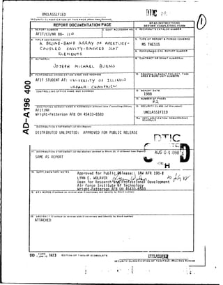
  • 1. UNCLASSIFIED 9i~~' SECURITY CLASSIFICATION OF THIS PAGE (When DaaeEntered),____________________ h REPORT DOCUMENTATION PAGE BEFR COSTPLETINSOR I. RPOR NUM3ER2. GOVT ACCESSION HO. 3. RECIPIENT'S CATALOG NUMBER 4. TITLE (and Subtitle) S. TYPE OF REPORT 6 PERIOD COVERED A, 1(A--BND iP ,LUPY 09 AKILTURZE- MS THESIS CCU?LEO CAV 9- b CKVD ,5LOT S. PERFORMIVIG ORG. REPORT NUMBER 7. AUTHOR(.) 5. CONT RACT OR GRANT NUMBER(.) 03Ef .H CMAr-H -. t3'JPNkS 9PERFORMING ORGANIZATION NAME AND ADDRESS 10. PROGRAM ELEMENT.' PROJECT. TASK AREA & WORK UNIT NUMBERS AFIT STUDENT AT: LUoi vus iTy O :ILL) 001- CONTROLLING OFFICE NAME AND ADDRESS t2. REPORT DATE 1988 13. NUMBER OF PAGES MONITO'NING AGENCY NAME 81 ADDRESS(If different from Controlling Office) IS. SECURITY CLASS. (of this. rePort) AFIT/NR UCASFE SWright-Patterson AFB OH 45433-6583 UNa DCLASSFIEIODONRDG SCNHEDULE ~I DISTRIBUTION STATEMENT (of this Reporl) < DISTRIBUTED UNLIMITED: APPROVED FOR PUBLIC RELEASE 17. DISTRIBUTION STATEMENT (of the abs tracfente red o in lnc 20, If different from Repor t AUG 0 4 988 SAME AS REPORT 1SUPPL-EMENTARY NOTES LYNNve E. r WOLAVERlease:j) IAW AFR 190-1 Dean for Research an4'Prote-ssional Develomn Air Force Institute f Technolog Wright-Pattcerso AFBOH 45433-6S83 19. KEY WORDS (Continue on reverse side If necessary ttd Identify by block number) 20. ASSTRACT (Conntinue on reverse side It necensary and Identify by block number) ATTACHED DID I O F 1413 EDITION OF I NOV 65 IS OBSOLETE JtCLJjjUE SECURITY CLASSIFICATION OF TNIS PAGE (When Date Entered)
  • 2. ABS TRACT A Broad-Band Array of Aperture-Coupled Cavity-Backed Slot Elements A broad-band array of aperture-coupled cavity-backed slot (CBS) elements was designed, constructed and tested. The antenna array design incorporated two major departures from previous CBS arrays: aperture coupling, and 'half-width' cavities. Expiremental results demonstrated these departures enhance the po- tential for larger operating bandwidths using less physical space than pre- vious arrays of CBS elements. Computer simulation and test results also in- dicated that the antenna array was not hindered by the presence of a large structural stopband such as was observed in all previous CBS arrays. Con- sequently, modulation of the antenna feedline impedance was not required for satisfactory performance. Antenna patterns for the array were similar over the frequency range 1.75 - 3.5 GHz. ceessicn For DC sT.ki E AvailabilJity i '4 U A,9 "an2lor ua.'st $ iproclal
  • 3. A BROAD-BAND ARRAY OF APERTURE-COUPLED CAVITY-BACKED SLOT ELEMENTS BY JOSEPH MICHAEL BURNS B.E.E., AUBURN UNIVERSITY, 1981 THESIS Submitted in partial fulfillment of the requirements for the degree of Master of Science in Electrical Engineering in the Graduate College of the University of Illinois at Urbana-Champaign, 1987 Urbana, Illinois
  • 4. iii ACKNOWLEDGEMENTS There are many besides the author who made this paper possible. The author wishes to thank his advisor, Professor Paul E. Mayes, for his superb guidance, patience, and prodding. He would also like to express his appre- ciation to Jeff Kromer for expertly building the antennas discussed herein; Jim Drewniak for his training in antenna design, construction and testing; Hugh Smith, Tom Sons, and Dave Tammen for sacrificing countless hours in an effort to obtain antenna patterns for this report; and all the other people in the Electromagnetics and Electromagnetic Communication Laboratories who helped with this research over the last year. In addition, the author would like to thank his office mates, Captain Charles F. Smith and Captain Mark A. Mehalic, for their assistance with the computer programs in the appendices of this report. Others whose help contributed to this research include the Air Force Institute of Technology, who paid the author's tuition and fees; TRW, Incorporated, who provided funding (a portion of which went directly to this work) for research on slot antennas; and Professor Weng C. Chew, whose enthusiastic, enlightening and patient teaching of an early electromagnetics course sparked the author's interest in this subject. Of course, the author wishes to express loving thanks to his wife Cindy, and their children Melissa, Amanda, Daniel, and Timothy for their support, understanding, prayers, and love. Finally, and most importantly, the author wishes to thank Almighty God for demonstrating many times during this work that 'I can do a1 rhin-- tbrnc:gh Christ who gives me strength.'
  • 5. iv TABLE OF CONTENTS CHAPTER Page 1. INTRODUCTION .......... ......................... . 1 2. ANTENNA DESIGN AND CONSTRUCTION ....... ............... 3 2.1 Szmurlo's Antenna .......... .................... 3 2.2 Cavity Design ........... ...................... 5 2.3 Cavity Construction ....... ................... . 11 2.4 Aperture Coupling ....... .................... . 11 3. PROTOTYPE I .......... ......................... . 14 3.1 Prototype 1 Construction ...... ................ 14 3.2 Prototype 1 Testing Procedure ..... .............. 15 3.3 Advantages of Aperture Coupling .... ............. . 16 3.4 Prototype I Data and Analysis ..... .............. 17 3.5 Conclusions from Prototype I Testing ... .......... 25 4. OTHER PROTOTYPES .......... ...................... 26 4.1 The High Frequency Anomaly ..... ............... 27 4.1.1 Determining the cause ..... .............. 28 4.2 Further Testing of Prototypes 2, 3, and 4 .. ........ . 35 5. LOG-PERIODIC ARRAY OF APERTURE-COUPLED CAVITY-BACKED SLOTS . . 36 5.1 Feed Network/Cavity Bottom Design and Construction . . 36 5.2 S Parameter Measurement ...... ................. . 40 5.3 Antenna Array Pattern Measurements ... ........... . 43 6. COMPUTER SIMULATION AND STOPBAND ANALYSIS ... ........... 49 6.1 The Shorted-Stub Model of a Single Cavity .. ........ . 49 6.2 Location of the Structural Stopband ... ........... . 52 6.3 Eliminating the Structural Stopband ... ........... . 55 6.4 Effect of Eliminating the Structural Stopband on Antenna Impedance ...... .................. 56 6.5 Cause and Impact of the Narrow Stopband ............. 9 7. CONCLUSIONS AND RECOMMENDATIONS ...... .............. 62
  • 6. V APPENDICES ........... .......................... 64 A: COMPUTER PROGRAM TO CALCULATE S PARAMETERS OF SHORTED STUB MODEL ....... .................. 64 B: COMPUTER PROGRAM TO LOCATE THE STRUCTURAL STOPBAND . . . . 66 C: COMPUTER PROGRAM TO DETERMINE THE IMPEDANCE OF THE MODULATED LINE ........ .................... 69 D: COMPUTER PROGRAM TO CALCULATE THE S PARAMETERS OF A LPCBS ARRAY ........ ..................... 72 E: COMPLETE ELEVATION PATTERNS OF 11 CAVITY ANTENNA ARRAY BY FREQUENCY AS MEASURED IN ANECHOIC CHAMBER ........ .. 76 REFERENCES ........... .......................... 81
  • 7. vi LIST OF TABLES Table Page 3.1 PROTOTYPE 1 - PARAMETERS OF INTEREST .... ............ 19 3.2 POWER DISTRIBUTION AMONG ARRAY ELEMENTS, T 0.92 COUPLING SLOT LENGTH - 4.5 cm ...... ................ 24
  • 8. vii LIST OF FIGURES Figure Page 1. Szmurlo's antenna [51 ..... .. .................... 4 2. Closed cavity, d << X .......... .................... 5 3. Top view of cavity with H wall ........ ................ 7 4. Top view of modified cavity ........ ................. 7 5. Modified cavity with slot ......... .................. 8 6. Exploded view of completed antenna ..... ................. 12 7. Aperture coupled cavity-backed slot antenna .. ......... ... 13 8. (a) S11 - Szmurlo's cavity 6 [51 ..... ............... ... 17 (b) S11 - Prototype 1, coupling slot length = 11.45 cm . . .. 17 9. S1I and S2 1 - Prototype 1, coupling slot length: 4.5 cm, coupling slot position: against cavity wall opposite radiating slot .......... ........................... 18 10. Efficiency versus frequency; coupling slot length = 4.5 cm . . 21 11. Antenna array with T - 0.92. To determine size of smaller cavities, multiply dimensions of right-most cavity by (0.92)m. 23 12. (a) S11 - Prototype 2. (10.6 - 11.4 GHz) ... .............. 27 (b) S21 - Prototype 2. (10.6 - 11.4 GHz) .... .......... ... 27 13. Sii - Prototype 2 with plexiglass clamps. (10.6 - 11.4 GHz).. 28 14. S1 1 - Prototype 2 with shallower slot. (10.6 - 11.4 GHz) . . 29 15. S11 - Prototype 3. (6.5 - 8.5 GHz) .... ............. ... 29 16. S11 - Prototype 3 with 15 mil thick microstrip feed. (6.8 - 8 GHz) .......... ........................... 30 17. (a) TDR - Poorly matched line ...... ................ .. 31 (b) Return loss - Poorly matched line .... ............ . 31 18. Return loss - Through ........ .................... . 32 19. (a) TDR - Reference short ....... ................. ... 33 (b) Return loss - Reference short ..... ............. ... 33 20. (a) S1I - Prototype 3 ........ .................... . 34 (b) Return loss - Reference short ..... .............. . 34
  • 9. viii Figure Page 21. Section of meandering line between two coupling slots . ... 38 22. Eleven cavity array feedline ...... ................. . 41 23. Measured SlI - 11 cavity array ..... ............... 42 24. Measured S2 1 - 11 cavity array ..... ............... 42 25. SIl - Szmurlo's 6 cavity array with unmodulated feed. (Frequencies in MHz) ... ........... . 42 26. Azimuthal patterns for 11 cavity array .... ............ . 44 27. Elevation patterns for 11 cavity array .... ............ . 46 28. Shorted-stub model of cavity [5] ...... ............... 49 29. (a) Computed S11 using cavity model .... ............. 50 (b) Measured S1j - Prototype 1. (0.75 - 2.25 GHz)......... ... 50 30. Model of cavity being fed by a modulated microstrip feed [5] . 51 31. jZif versus f (GHz) - Element 7 with unmodulated feedline 53 32. Phase versus f (GHz) - Element 7 with unmodulated feedline 54 33. Phase versus f (MHz) - Szmurlo's cavity 6 .. .......... . 55 34. JZij versus f (GHz) - Element 7 with modulated feedline . . 57 35. Phase versus f (GHz) - Element 7 with modulated feedline . . . 57 36. Computed S11 - 11 cavity array with unmodulated feedline. (1.0 to 4.5 GHz) ...... .................. . 58 37. Computed S 11 - 11 cavity array with modulated feedline. (1.0 to 4.5 GHz) ...... .................. . 59
  • 10. CHAPTER 1 INTRODUCTION In recent years, there has been a burgeoning interest in low-profile, wide-band antennas. Low-profile antennas have numerous applications, espe- cially for missiles and aircraft, because only these antennas can be con- formally mounted. The most popular types of thin antennas are the microstrip patch and the cavity-backed slot (CBS). Much research has been done on both types, but the project reported herein involves only CBS antennas. The main objective of this research is to extend the operating bandwidth of a log-periodic (LP) array of thin CBS elements. Research on CBS antennas dates back more than thirty years. Mayes provides a good summary of early research and recent progress in developing low-profile, wide-band CBS antennas in his report Very Wide Band Antennas for Missile Fuze Applications [1]. One problem encountered in early attempts to design log-periodic arrays of CBS elements was the structural stopband which occurs in a periodic array of such elements. In this band of frequencies there is no propagation down the feedline. When a corre- aponding region of attenuation occurs between the feedpoint and the active region of a log-periodic cavity-backed slot (LPCBS) array, the wave launched at the input is mostly reflected before it reaches the active (radiating) region. The structural stopband is caused by additive reflec- tions from discontinuities presented by the slots. Ingerson and Mayes [2] found that modulating the feedline impedance was an effective way of elimi- nating the stopband. Building on their work, Ostertag [3] designed an LPCBS array using smaller cavity depths and obtained a 50 9 mean impedance through use of a computer-synthesized modulated impedance feedline. More
  • 11. 2 recently Tammen's research [41 focused on eliminating the structural stop- bands associated with many LP antennas by combining CBS and monopole ele- ments. Finally, Szmurlo [5] concentrated on increasing the bandwidth of an LPCBS array while using very thin cavities of constant depth and optimizing the design of the modulated impedance feedline. The bandwidth achievable by antennas of his design is limited because of the immense amount of space they require. The goals of this research were to design and build an LPCBS antenna which has a larger operating bandwidth, uses less 'real estate', and oper- ates at much higher frequencies with a larger power gain than previous LPCBS arrays. Achieving these goals requires taking several large steps forward from the work done by Szmurlo. First, in an effort to reduce losses, the antenna was designed to have air-filled cavities rather than Rexolite-filled ones. Second, the cavities were to be excited by aperture coupling, that is, energy would be coupled into the cavity through an aper- ture in the bottom of the cavity rather than through the radiating slot in the top of the cavity. Third, a new theory would be applied that allowed each elemental cavity to be built only half as wide as Szmurlo's elemental cavities. This theory and application will be discussed in more detail in Chapter 2. Finally, it was desired that this new antenna would operate at higher frequencies than any previous LPCBS. The high frequency testing of the new antenna led to previously unseen problems, as will be pointed out in Chapter 4.
  • 12. 3 CHAPTER 2 ANTENNA DESIGN AND CONSTRUCTION Before constructing an LP array of CBS antennas that introduced several new departures from the previous case, it was considered prudent to test several prototype elements. From the testing of these prototypes, the scaling factor (T) and many other useful design criteria used in the LP array were determined. This chapter will focus on the design and construction of these proto- types. The testing of these prototypes and the selection of design cri- teria will be discussed in detail in Chapters 3 and 4. 2.1 Szmurlo's Antenna Since this research was, in many ways, a continuation of Szmurlo's, it is useful to have a more detailed understanding of his antenna. A descrip- tion from his thesis follows. The antenna was constructed from a I/P-inch sheet of Rexolite 2200. An aluminum sheet (also 1/8 inch) was used a, backing for the Rexolite to provide support and to pro- vide threaded holes for the screws. The brass screws that form the vertical cavity walls were approximately 1/2 inch apart for the four largest cavities and about 3/8 inch apart for the remainder. These spacings had been determined ade- quate to make the S-parameters of an isolated cavity-backed slot with screw walls agree very well with those of one with solid walls. Copper cladding forms the top and bottom walls. A slot was cut into the top cavity wall by removing the copper cladding to allow the cavity to radiate when excited. A drawing of the cavities formed on the Rexolite is shown in Figure 1. To excite the cavities, a microstrip feed is passed over the slot of each cavity. It was found that for symmetrical pat- terns, the slot should be fed from the center. The feedline was constructed on a 1/16-inch sheet of Rexolite 2200. The characteristic impedance of the feedline was trimmed to 50 ohm
  • 14. 5 by observing its response when tested with a TDR. After using the TDR, Lhe copper ground plane of the feed was cut away where it would lay over the cavity slot. Good contact between the ground plane and the cavity top wall must be maintained, particularly in the vicinity of the slot, or antenna performance will degrade. A type N female bulkhead connector is present at both ends of the feed. This allows for the measurement of reflection and transmission coefficients of the antenna [5]. The antenna built by Szmurlo operated from 975 to 1325 MHz. 2.2 Cavity Design As mentioned previously, the antenna was designed utilizing a theory that allowed each elemental cavity to be built half as wide as elemental cavities in previous CBS antennas. This theory was first proposed by Tanner [6]. The basis for the bisection of the cavity can be seen by first analyzing a closed cavity which is very thin (as compared to a wavelength) in the z direction as shown in Figure 2. Z d0 Fub y .x ~Figure 2. Closed cavity, d <( A.
  • 15. 6 For the transverse magnetic (TM) case, the time-harmonic (ej wt timp dependence suppressed) fields inside this cavity can be written as: E - E sin mx sin nly [7] (2.1) z mnp a b -j mnp I i n) Eo (ncos (71 (2.2) (mlr)2 m 2 sin -a (S jwe E mr Cos mrx) sin [71 y (mw)2 nn 2 aa bo [(3 where the z dependence has been dropped because of the thinness in the z direction. Substituting the equation for Ez into the Helmholtz equation, (V2 + B2) E - 0, yields the dispersion relation 2 O (mx)2 + (2.4) Solving this equation for w yields 1 mst 2 +n 2 1/2 w nm) / - a (2.4a) which is the resonant frequency of the mn mode of this cavity. One can also note from the field equation E (with m - n = 1) that as x is held z constant and y is varied, E reaches a maximum at y - b/2. Furthermore, at z y - b/2, Hx - 0 for the TM110 mode. Thus, an H wall (a surface along which HRTAr - 0) can be inserted in the plane (x, b/2, z) without interfering with the fields of the cavity. (Note: in most previous rectangular CBS anten- nas, the radiating slot was placed along the line (x, b/2, d)). A top view of this cavity with the H wall inserted would look like Figure 3.
  • 16. 7 X 4--H Wall -- E Wall zI b/2 Y Figure 3. Top view of cavity with H wall. Next, consider a cavity that has a top view much like half of the cavity in Figure 3. Pictorially, a top view of this cavity would look like Figure 4 below. x 1-H Wall E Wall Z b/2 y Figure 4. Top view of modified cavity.
  • 17. 8 One three-dimensional realization of this cavity is shown in Figure 5. Z x - - hls -Slot in Cavity Top b/2 Y X Figure 5. Modified cavity with slot. To determine the field equations of this modified cavity, begin with the phasor form of Maxwell's equation - V z Z Ez J wu0H (2.5) or, using rectangular coordinates and writing the curl as a determinant yields ax ay az i" 0 H (2.6) o 0 E z aEZ aE + ay a " 0 H (2.7) zE aE Therefore --- 3- ( E-z x 28Z) J1 ax a (2.8) L0
  • 18. 9 To find E , use the Helmholtz equation. zz [V2 + w2 o0co0] Ez .0(2.9) This equation admits solutions of the form 0 sin x f sin Byy ( cos E o [8] (2.10) Cos 0yy Cos Byy where only one solution in each of the brackets must be selected. (Note also that the variation with z has again been dropped because of the thin- ness of the cavity in the z direction.) To determine which solutions to select, consider the boundary conditions EZ (x, 0, 0) --0 (2.11) Z E (0, y, 0) = 0 (2.12) a EZ (-a, y, 0) = 0 (2.13) H (x, b/2, d) - 0 (2.14) x It is apparent from the first two boundary conditions that the only admissible solution for E is Ez - E sin $ x sin 8yy (2.15) From the third boundary condition, it is clear that sin 8x (-a) = 0 or =--- IF Bx (2.16) Now, the magnetic field can be calculated from (2.8) -8y H " (E° sin (SxX) cos (6yY)] (2.17) Hx jW 0 0 x o The fourth boundary condition states that Hx (x, b/2, d) = 0. Therefore, mm m fmmmmmmmm~ - -- "
  • 19. 10 8 b/2 n- nodd or Sy. (nZ); n odd (2.18) Substituting (2.16) and (2.18) into (2.15) yields E = E sin ( ) sin (.) (2.19) 2 Substituting (2.19) into (2.9) and solving for W ioCo0 give 2 (37r2 niT)2 (2.20) o , + which is the dispersion relation for the modified cavity. Solving (2.20) for w yields = n I [m(RI) 2 + (n T2]1/2 2.21) mn - aI- ''J](.1 / Uo Eo which is the resonant frequency for the mn mode of this modified cavity. Rewriting some of the important equations for the modified cavity: Em E sin (--) sin (fly) (2.22) H- /b [E sin (") cos (2.23) 1 mir2 nn 2 1 /2 W 1 [ (-) + (a-)] (2.24) Mn O a b Note that these three equations for the modified cavity are of the same form as (2.1), (2.2) and (2.4a) for the closed cavity of Figure 2. In fact, (2.24) and (2.4a) are exactly alike. Thus, a cavity can be created that is one half as wide as the closed cavity of Figure 2 (and still have
  • 20. 11 the same resonant frequency) by extending a slat across the top of the cavity as shown in Figure 5. This is an extremely encouraging result because it means that an array of modified cavity antennas (of the type in Figure 5) can be built in about half the space of the previous arrays which used unmodified cavities (of the type in Figures 1 and 3). The antennas tested during this research were all designed in accordance with Figure 5 for a specific resonant frequency as given by (2.24). 2.3 Cavity Construction In general, the prototype cavities were constructed by milling 1/16" deep into a 1/8" brass sheet. The length and width of the cavities were determined by Eq. (2.24) with m = n - I since we are interested in using the TMI1 0 mode. The radiating slot was cut along the length of one edge of the cavity. At this point, the sides, top and radiating slot (in the top of the cavity) were completed. The bottom of the cavity was a sheet of double clad 1/16" Rexolite (E = 2.6) fastened to the cavity body r by brass screws tapped into the 1/8" brass. Figure 6 illustrates an exploded view of the completed antenna. 2.4 Aperture Coupling To turn this slotted cavity into an antenna, energy must somehow enter into the cavity and be radiated out the radiating slot in the top. In the past, this was usually done by either inserting a probe in the bottom of the cavity, or running a microstrip line across the radiating slot as Szmurlo did (see Chapter 1). Instead of using one of these traditional
  • 21. 12 ,,.. z e. -. 14% S101 0 0 0 0 ln¢o /A Figure 6. Exploded view of completed antenna. methods to feed these cavities, a new approach was used: aperture coupling. In aperture coupling, one side of the double-clad Rexolite is the cavity bottom. On the other side, the copper cladding is peeled away except for a strip of a specific width (4.4 mm for 50 in 1/16" Rexolite) which acts as the antenna feedline. On the cavity bottom side, a narrow, short strip of copper orthogonal to the feedline (which is on the other side) is peeled away to form the coupling aperture (or coupling slot). An example of an aperture coupled cavity-backed slot is shown in Figure 7. Aperture coupling has some advantages over the more traditional methods of feeding the cavity. For one thing, it is a flatter system of feeding the antenna than probe feeding and thus is better suited for conformal mounting. Additionally, aperture coupling does not interfere with the radiation of energy through the radiating slot. When the same slot is used for both coupling and radiation, this interference (scattering from
  • 22. 13 Radiating Slot Copper Cavity Coupling Aperture (Slot) Ground Plane (Bottom) - ------ Feed Line i. Rexollte (E?:2.6) 1/16" Figure 7. Aperture coupled cavity-backed slot antenna. the feedline) is unavoidable. With aperture coupling, the feedline can be placed anywhere along the slot (not just the center) without affecting the antenna patterns. Finally, aperture coupling offers a new degree of freedom, variation of the coupling aperture size, not available heretofore. On the other hand, when aperture coupling is used, some radiation will leak out the coupling aperture. Thus, power gain may be lower when aperture coupling is used. Aperture coupled antennas are relatively new devices. Pozar [9] first proposed the concept for exciting microstrip patch antennas in 1985. Since then he and others, notably Sullivan and Schaubert [1I, have investigated, with some success, the use of aperture coupling with simple microstrip patch antennas. However, until now, aperture coupling has not been used to drive cavity-backed slot antennas.
  • 23. 14 CHAPTER 3 PROTOTYPE 1 In this chapter, the first prototype antenna and initial testing will be discussed. Four prototypes were constructed and tested: one that was the same size as the largest cavity in the array (Prototype 1), one the same size as the smallest cavity in the array (Prototype 2) and two others in between the largest and smallest cavities (Prototypes 3 and 4). The testing on Prototype 1 was by far the most conclusive. The results of various tests on this prototype were used to establish the length and posi- tion on the cavity bottom of the coupling slot as well as the antenna array scaling factor (T). Testing on Prototypes 2 and 3 had some unexpected results, which will be discussed in the next chapter. 3.1 Prototype 1 Construction Prototype I was built to the specifications of Figure 5 with a = 10 9/16" (26.829 cm), b/2 1 1 17/32" (3.889 cm), and W . 5/32" (0.3969 cm). 5 The cavity bottom/feedline was constructed of 1/16" Rexolite (e = 2.6). r On the feedline side, all the copper except a narrow strip (the feedline) was removed. The width of the strip (4.4 mm) was determined by formulas proposed by Edwards [11] for the given height (1/16") and a characteristic impedance of 50 ohms. SMA connectors were attached to each end of the line. The line was tested on a TDR and trimmed for a good match. The coupling aperture was then cut in the middle of the other side of the Rexolite with the arbitrarily selected width of 2.5 mm and length 11.45 cm. The length of the coupling slot was easily varied by covering portions of the 11.45 cm opening with copper tape. The position of the coupling slot
  • 24. 15 in the cavity bottom was also variable by simply loosening the connecting screws and sliding the cavity bottom in either direction. To determine the resonant frequency of this cavity, its dimensions were substituted into Equation (2.24). This substitution resulted in a resonant frequency of 12.615 x 10⁹ rad/s or 2 GHz. For a closed cavity of these dimensions, a resonant frequency of 2 GHz would be expected. But, in fact, (2.24) assumes that W - 0 (which it is not) and does not take into S account the coupling aperture. Therefore, it was expected that the actual resonant frequency of Prototype I would be proportionally less than 2 GHz with the increase in size of the apertures. 3.2 Prototype 1 Testing Procedure To test Prototype 1, and the other prototypes as well, the following sequence of steps was followed using the HP 8510 Network Analyzer. 1) Using the calibration kit, a calibration over the frequency range of interest was executed. 2) The measurement plane was then shifted to coincide with the coupling aperture. For reflection measurements, this was accomplished by using a reference short. The short was constructed similar to the microstrip feed line except it was only half as long and had a shorted plane on one end. Thus, the electrical distance between the shorted plane and the connector was equal to the electrical distance between either connector and the coupling slot of the microstrip feed line. The short was connected to the HP 8510 and electrical delay and phase mamlm~ i Imi ( H ( ( m ms
  • 25. 16 offset were added until the trace (S1) on the 8510 collapsed to a point at the left edge of the Smith chart on the real axis. Similarly, electrical delay and phase offset were added to transmis- sion measurements via a reference 'thru' (which was the cavity bottom/ feed line with the coupling aperture covered with copper tape). 3) Finally, the antenna itself was connected to the 8510 (with the values of electrical delay and phase offset gained through step 2 above programmed into the 8510) as a two-port device and measurements recorded of S11 and S21. 3.3 Advantages of Aperture Coupling Once the first two steps were completed for the cavity bottom/feed line and cables (from 8510 to antenna), numerous measurements as described in step three were made with the length and position of the coupling aper- ture as variables. As expected, the longer the coupling slot, the lower the resonant frequency (as indicated by a crossing of the real axis by SI). Furthermore, as the coupling slot was shortened, the size of the S locus shrunk toward the center of the chart. The impact of this phe- nomenon can best be seen by comparison of Prototype I data with Szmurlo's single cavity data. Figure 8a is the S I data for Szmurlo's Cavity 6. Note the similarity between the shape of the locus in Fig. 8a and that of Fig. 8b, the S1 data for Prototype i with a coupling slot length of 11.45 cm. Neither Szmurlo's Cavity 6 nor Prototype 1 (in this configuration) is a very well-matched radiator (as evidenced by the large distance between the center of the chart and the crossover point on the real axis at resonance).
  • 26. 17 Figure 8a. Figure 8b S11 - Szmurlo's cavity 6 [5). S11 - Prototype 1, coupling slot length 11.45 cm. Figure 9 shows the S11 and $21 locus for Prototype 1 with the much shorter coupling slot length of 4.5 cm. Note that the S locus of this figure indicates a much better match than the antennas of Figure 8. This ability to affect the antenna impedance by varying the length of the coupling slot is exciting because it gives the antenna engineer a degree of freedom not previously available. Conversely, the position 3f the coupling slot had virtually no effect on the resonant frequency or the shape of the S1 and S21 loci. 3.4 Prototype 1 Data and Analysis As stated earlier, the purposes of testing the first prototype included determining the optimum length of the coupling aperture and the optimum scaling factor for the log-periodic array. The performance factor
  • 27. 18 MARKER MARKER 1. 77 5 1.7I 5-ki "-. " " - .,-. [__ _ . .. . . . . .-- -. _ -_ , START - 6. 00 ThGO@ t START 6. 73e6"6 C43 STOP 2z9966@6 C34Z 51W 2. 2"6000 own Figure 9. S11 and S2 1 Prototype 1, coupling slot length: 4.5 cm, coupling slot position: against cavity wail opposite radiating slot. that was used to determine the optimum was the upper bound on the radiation efficiency as defined by e , 100 1 - "l 2 _ Is21 2 % (3.1) Rt I -llol isz Il 2.I A close look at this aqcation reveals that the numerator represents the part of the signal that is neither reflected nor transmitted; this is the portion of the signal that is radiated (discounting losses). The denomina- tor, on the other hand, represents the portion of the signal that is not reflected; this is the sum of the radiated and transmitted portions of the signal. Hence, (3.1) could be rewritten as eR 100 radiated (3.2) relctd hi sth u Rh radiated n transmitted otoso h
  • 28. 19 Thus, eR is the percentage of the signal remaining after reflection that is radiated. It was decided that a radiation efficiency at resonance of around 60% would be best for application to a log-periodic array. The reason is that no single element in the array should radiate so much of the signal that there would not be enough signal left to excite remaining ele- ments. If e >> 60%, the active region of the array would be made up of r just one or two elements. With this in mind, the data from Prototype I testing were examined to see how the efficiency changed as a function of the coupling slot length. As expected, the efficiency declined as the length of the coupling slot shortened, most likely because less energy is coupled into the cavity as the coupling slot becomes shorter. The antenna performance with the three specific coupling slot lengths that yielded an efficiency of around 60% was then closely scrutinized. Table 3.1 lists the parameters of interest of these three configurations. TABLE 3.1 PROTOTYPE I - PARAMETERS OF INTEREST Coupling Slot Resonant eR M Length (cm) Freq. (GHz) 5 1.655 72.38 4.5 1.78 53.643 4 1.86875 50.64
  • 29. 20 To determine which of these three coupling slot lengths to choose, and to simultaneously determine the scaling factor, a power distribution analysis much like that done by Tammen for his log-periodic array of monopole-slot elements was performed [4]. The goal of this analysis was to determine how power would be distributed among the elements of the log periodic array at different frequencies for a given scaling factor (and in our case, a given coupling slot length). With this result a scaling factor can be selected which, for a given frequency, will produce an adequate number of elements with relative power above a desired threshold. The elements above the threshold will be those that make up the active region of the antenna for that frequency. In a nutshell, the analysis consists of creating an efficiency versus frequency curve for each cavity in the array. Then, for a given frequency, the e versus f curve of the smallest cavity can be used to determine what percentage of power incident on this first cavity will be radiated. Next, the e versus f curve for the second smallest cavity is used to determine what percentage of the remaining power is radiated by this second cavity, and so on. Since it was too difficult to generate an e versus f curve for each cavity, it was assumed that the curves for all the cavities had the same shape. To obtain an e versus f curve for the higher frequency cavi- ties, the frequencies of the e versus f curve for Prototype I were simply scaled. For individual log-periodic elements, one could expect this scaling to be accurate. The fact that the cavity depths in our array are not log-periodically scaled should have little impact. Mayes found that efficiency versus frequency characteristics for shallow cavities did not change much with small changes in cavity depth [12].
  • 30. 21 A methodical example will serve to more clearly explain the analysis described above. For this example a coupling slot length of 4.5 cm and a scaling factor of T - 0.92 was used. The steps in the analysis follow: 1) Generate an efficiency versus frequency curve for the con- figuration of interest (e.g., Prototype 1 with a coupling slot length of 4.5 cm) using iSII I and is211 from the HP 8510 and Equation (3.1). Figure 10 shows the curve generated for this example. 70_ 60 Resonance 50 0) 40- 30- 20 16 12 1.78 8 1 1 1 1 1 1 I 1 1.3 1.5 1.7 1.9 2.1 f (GHz) Figure 10. Efficiency versus frequency; coupling slot length = 4.5 cm. 2) Determine the number of cavities, n, in the required array band- width. Since an electrical bandwidth of 5:1 was desired, it was felt that a structural bandwidth of 6:1 was needed. To achieve a 6:1 structural bandwidth with T = 0.92 indicates that for any
  • 31. 22 dimension Xo, of the largest element, the smallest element will m have that dimension equal to 6 X (0.92) , i.e., 0 6 X (,. 9 2 ) m - X 0 0 0.92 m , 1/6 log (1/6) - 21.489 m log (0.92) - number of other elements in addition to the first element. Therefore, 22 elements were needed to achieve a 5:1 electrical bandwidth with a scaling fac- tor of 0.92. A drawing of such an array is shown in Figure 11. 3) Generate a power distribution table (see Table 3.2). a) Translate a particular frequency of interest by multiplying it by (0.9 2 )m (where m is the exponent referred to in Figure 10). Start with the highest m in the array and continue to chaage m until the translated frequency (ft) is greater than or equal to 1.25 GHz, the lowest frequency of Figure 9. (Alternatively, solve m = log fre 2 5 GHz itrest) / log(Q.92) and round up to find the highest m which yields a translated frequency above or equal to 1.25 GHz.) b) From Figure 9, find the value of e corresponding to f and t place it in a table (e.g. Table 3.2) where f and m intersect. c) To find the fractional power for the m-I element, use the following formula from Tammen [4) i-I FPi - e, [100 - I FPn ] nml
  • 32. 23 ' -. E • ,,.4 .- , F. , 0 e' 0 ~ 0 -- -4. .,o .~--- - , ,-4 >i m.m i i i i
  • 33. 24 - - I -o 0 N ON- . . . . . , . - . . . . . . N ~'caz --
  • 34. 25 where FPi is the fractional power of the ith element, FP is the i n fractional power of the nth element and ei is found from Figure 9 by using ft/. d) Repeat previous steps until the whole line for the frequency of interest is filled in (see Table 3.2). Once the previous steps are completed over a range of frequencies, the power distribution table can be completed. Several tables for different scaling factors and different coupling slot lengths were created in this manner. Based on previous research, it was decided the active region for a given frequency needed to have at least three elements with relative power above 10. The table with the greatest bandwidth of frequencies that had three or more elements with relative power above 10 was selected. That table corresponded to a r of 0.92 and a coupling slot length of 4.5 cm. It is reproduced in this report as Table 3.2. 3.5 Conclusions from Prototype I Testing Many valuable things were learned from testing Prototype 1. First of all, the data verified the theory of bisecting the traditional rectangular CBS. Second, the 'optimum' coupling slot length for Prototype 1 was selected via power distribution analysis. Finally, and most importantly, a new benefit of using aperture coupling was realized. That is, the perfor- mance of the prototype antenna (and presumably the performance of the entire array) can be controlled, in part, by the length of the coupling slot.
  • 35. 26 CHAPTER 4 OTHER PROTOTYPES It was decided that a second prototype should be built and tested in order to see if scaling the antenna altered the performance parameters observed for Prototype I. This second prototype was designed to have the same dimensions as the smallest element of the antenna array. Based on the theory of scaling, its resonant frequency was expected to be approximately 11 GHz, an order of magnitude higher than any previously tested CBS antenna. Since the wavelength shrinks proportionally as the frequency rises, much greater attention to detail was used when constructing and testing this higher frequency device than was used when building and testing Prototype 1. Nevertheless, problems were anticipated and a major problem was encountered during preliminary testing of Prototype 2. The basic problem was that the impedance locus of S11 moved in a coun- terclockwise (instead of clockwise) direction as frequency increased (Fig. 12a). Interestingly, the $21 locus (Fig. 12b) was normal (clockwise). When further testing of Prototype 2 did not reveal the cause of the anomaly, a third prototype with a resonant frequency intermediate to those of Prototypes I and 2 (fr - 7.35 GHz) was constructed and tested. Unfortunately, Prototype 3 also manifested the unexplained phenomenon. A fourth prototype with a resonant frequency still lower than that of Prototype 3 was constructed and tested (fr . 3.77 GHz); the problem was not observed for this final prototype. Eventually, the cause of this frequency-related phenomenon was discovered. This chapter will detail the problem, the steps taken in search of the cause, the cause, and the solution to the problem.
  • 36. 27 4.1 The High Frequency Anomaly Recall from Prototype 1 data (Figure 9) that both the S11 and $21 loci travel clockwise (CW) around the Smith Chart as frequency increases. I 11. t -- - - , -- i " " . ,- -, , ' 4- .- -.. /;7, - -, / s-j- - ° /"-- .' /' -; ....-9/"<-".. Figure 12a. S11 - Prototype 2. Figure 12b. S21 - Prototype 2. (10.6 - 11.4 GHz) (10.6 - 11.4 GHz) The reason for this clockwise progression can be found in Foster's Reactance Theorem (FRT). This theorem states: "The slope of the reactance or susceptance for a loss-free one-port is always positive" [13]. Granted, by design an antenna is not lossless and those discussed here are two- ports. However, until Prototype 2 was tested, no antennas had ever seemingly violated this theorem.
  • 37. 28 4.1.1 Determining the cause As can be seen from Figure 6, the prototypical CBS antenna has very few components. It was decided, therefore, to change/alter different com- ponents of the antenna (one at a time) and observe the effect on the S11 trace. First, the metal clamps that held the microstrip feed in place were replaced with plexiglass clamps. As Figure 13 illustrates, this change had no effect. Figure 13. S11 - Prototype 2 with plexiglass clamps. (10.6 - 11.4 GHz) Next, the radiating slot was made more shallow. This change shifted the location of the trace, but not the shape of it (Figure 14). Before making any further changes, Prototype 3 was built to determine if this anomaly was also observed at slightly lower frequencies. As men- tioned earlier, Prototype 3 also displayed the counterclockwise phenomenon (Figure 15). It was then hypothesized that perhaps losses were responsible
  • 38. 29 for this effect and, therefore, an effort was made to reduce them wherever possible. The first step in this direction was to replace the dielectric Figure 14. S11 - Prototype 2 with shallower slot. (10.6 -11.4 GHz) 8.5 '-4 (6.5 -8.5 GHz)
  • 39. 30 in the prototype with a much thinner one (15 mils). In addition to reducing losses, this step was also taken to make sure that a quasi-TEM mode was still being propagated on the microstrip line, because as frequency rises, the microstrip height must shrink to ensure quasi-TEM propagation [i]. These modifications, however, had no impact on the counterclockwise phenom- enon (Fig. 16). To lessen losses still more, the RG-214 cables used as test port extensions from the 8510 to the antenna under test were replaced -"i I 8.0 , h- / - / Figure 16. Sll - Prototype 3 with 15 mil thick microstrip feed. (6.8 - 8 GHz) with precision semirigid cables. Although the S11 locus measured following this modification indicated less loss, it still proceeded counterclockwise with frequency. Again attempting to maximize performance and reduce loss, the connectors on the antenna were replaced by a myriad of different higher precision connectors. These changes had no effect on the problem.
  • 40. 31 Since alteration of virtually every antenna component had no impact on the direction of the S11 locus, it was concluded that something outside the antenna was the cause of the anomaly. Therefore, a closer examination of the reference through (which also acts as the microstrip feed) and reference short were made. In addition to the usual examination on the Time Domain Reflectometer (TDR) mode of the 8510, the return loss of the through and short was checked over a very wide bandwidth (0.0896 - 18.0 GHz). This was done because it was discovered that poorly matched lines often exhibit per- turbations in their return loss plots above a certain frequency. Figure 17 shows the TDR plot and return loss for a typical poorly matched microstrip line and the associated return loss plot. The hypothesis was that these perturbations indicated the propagation of higher-order modes which could Ref. -100.0 mUnits, 50.0 oUnits/dP- ' Ref. 0.0 dB, 10.0 dBldiv ! i iI IoI MARKER 1 .. .ARKER '3 400.0 psi 3.552272 G-H art7 -1.0 ns. Stop: 4.0 ns StaIrt: 0.0896 GHz. Stop: 18.0 GHZ Figure 17a. Figure 17b. TDR - Poorly matched line. Return loss -Poorly mitched line. cause the S11 locus to behave abnormally. Although this hypothesis was never confirmed during this research, the return loss plots did reveal
  • 41. 32 something interesting which ultimately pointed to the cause of the unusual S loci. The return loss plot for the through (Fig. 18) had no perturbations throughout the frequency raiige. This indicated the transmission line was probably not the source of the problem. The return loss plot of the short, however, was extremely abnormal. A short should have zero return loss for Ref. -20 dB, 10.0 dB/div C. - I I i J,[ I Start: 0.0896 GHz. Stop: 18.0 GHz Figure 15. Return loss - Through. all frequencies because Irl for a short is one. Although the reference short for Prototype 3 had the TDR plot of a good short (Fig. 19a), its return loss was not zero for all frequencies (Fig. 19b). In fact, there were a number of frequencies where its return loss was substantially less
  • 42. 33 R- . -500.0 mUnits, 200.0 mUnits/'4 Ref. -20.0 dB, 10 dB/div K-KR 2- LL i L I GHz 8.OGHz4 __ - 7.86GHzj StarL: -1.0 ns. Stop: -4.0 ns Scart: 0.0896 GHz. Stop: 18.0 Giiz Figure 19a. Figure 19b. TDR - Reference short. Return loss - Reference short. than zero. Note the two markers in Figure 19. They indicate the frequency range within which Prototype 3 was tested. Figure 20a shows the S11 locus for the third prototype when the measurement plane was established using the short of Figure 20b (Figure 19b repeated). The plot of Figure 2 0a is initially moving counterclockwise and then begins moving clockwise at about 7.8 GHz. In other words, the locus is abnormal from 6.5 - 7.8 GHz. A close examination of Figure 20b reveals that 6.5 - 7.8 GHz is the same range (within the 6.5 - 8 GHz band of Figure 20a) in which the return loss of the reference short is not equal to zero. It was concluded, therefore, that the cause of Che backward phenomenon was the inconsistency of the reference short in the frequency range of interest. Consequently, the measurement plane was also inconsistent
  • 43. 34 because the inconsistent reference short was used to establish its loca- tion. Simply put, the measurement plane for tne reflection measurements Ref. 0.0 dB. 10.0 dB/div 7 ., 6.5GHz i,;.8. GHz I I 7.86GHz Start: 0.0896 Gz. Stop: 18.0 GHz Figure 20a. Figure 20b. S11 - Prototype 3. Return loss - Reference short. was changing with frequency. This explanation also accounts for the fact that all of the transmission measurement plots (S2 1 ) were normal. Although the evidence already discussed was convincing, a different method of establishing the measurement plane had to be established and the effect of the new method on the S trace observed to validate the theory. Recall that the microstrip feed network doubled as the reference through and the coupling aperture was exactly in the middle of it. Thus, the electrical delay and phase offset we had established for the transmission measurements could also be used to establish the reference plane for the reflection measurements. This procedural modification was tested, and the resulting S11 locus did indeed move in the right (clockwise) direction.
  • 44. | !- 35 4.2 Further Testing of Prototypes 2, 3, and 4 The discovery of the cause of this anomaly allowed the research to move forward but the performance factors of the first two prototypes were never correlated because of equipment breakdowns and parts shortages. Since time was limited, it was decided to hypothesize that the performance factors would indeed correlate and to pursue the design, construction and testing of the antenna array.
  • 45. 36 CHAPTER 5 LOG-PERIODIC ARRAY OF APERTURE-COUPLED CAVITY-BACKED SLOTS The design of the log-periodic elements was accomplished by multiplying the dimensions of Prototype 1 by T m (= - 0.92; m is defined in Figure 11). Two dimensions, however, were not scaled: the cavity depth and the separa- tion between adjacent cavity walls. The cavity depth was not scaled in order to make construction of the array easier. Furthermore, as stated in Chapter 3, earlier research by Mayes indicated that variation in the depths of shallow cavities had little effect on their performance parameters; therefore, no impact was expected from this subtle deviation from true log- periodic design. Conversely, the separation distance between antenna ele- ments was not the result of a decision based on previous research and theory; it was a design flaw. Fortunately, the data presented in this chapter indicate that this design flaw had little, if any, effect on the frequency-independent performance of the antenna, although it did impact the design of the feeder and thereby limit the bandwidth of the antenna. The array elements were milled out of 1/8" brass to the specifications of Figure 11. The array feed network was constructed in the same manner as the prototype feedlines using 1/16" double clad Rexolite. However, the feed network for the array was designed much differently than were the pro- totype feedlines. This chapter focuses on the design and construction of the array feed network, the measurement of the scattering parameters, and the antenna patterns of the antenna array. 5.1 Feed Network/Cavity Bottom Design and Construction The design of the feed network was in large part dictated by the goal of having an antenna array that produced a backfire radiation pattern. To L
  • 46. 37 achieve backfire radiation, the waves radiated by the antenna elements must add in phase in the backfire direction. One successful method of obtaining this in-phase addition of radiated waves has been to ensure that the phase shift going from one element to another and back is equal to 2n radians [5]. In the case of this antenna array, the total phase shift is equal to that of the incident wave as it travels along the feedline from the coupling slot of one element to that of the next plus that of the radiated wave as it travels in free space back to the radiating slot of the first element. If the feedline followed a straight path between coupling slots, this phase shift would be less than 27. Therefore, excess feedline, of length d, must be added between coupling slots. Analytically, a formula for d can be derived as follows: 8 0d + Bd 211 radidns (phase difference (5.1) equivalent to dt = one wavelength) 2- 6od 231 - 6od r 0 1 211.. d. 1 (2L c - dJ Therefore d ___ d) (5.2) In Equation (5.2), d is the physical distancc between the radiating slots, Cr is the relative permittivity of the dielectric substrate of the feed network, c is the speed of light in free space, and f is the resonant frequency (as defined by scaling resonant frequency of Prototype 1) of the smaller of the two cavities.
  • 47. 38 If an infinite front-to-back ratio were desired, the feedline length would be designed so that the waves radiated in the direction of the inci- dent wave on the feedline would be 180 degrees out of phase. Because of time limitations, an infinite front-to-back ratio was not one of the goals of this research. The resultant section of line between any two coupling slots would have a displaced portion and a main-line portion as in Figure 21. 50%, 450 Mitre Displaced Portion in Accordance With [14] h Mainline Portion Coupling Slot m-1 -. I Coupling Slot mn h =Vertical Distance =1/2(d-d s ) Figure 21. Section of meandering line between two coupling slots. The whole feed network for the 23 cavity array was to be built using the design shown in Figure 21, but another problem arose. At higher fre- quencies (0 4.2 GHz), the distance, h, shrinks so much that the displaced portion and the main-line portion of the feedline begin to blend together. As the frequency continues to climb, h would eventually have to be a nega- tive quantity in order for Equation (5.1) to be satisfied. This fact pre- sents a problem because a negative distance is not physically realizable.
  • 48. 39 This problem is a result of the design flaw discussed in paragraph one of this chapter. If the antenna did not have this flaw, then the distance h of any given element would always be the scaled h of the previous ele- ment. To see this, rewrite Equation 5.2 and consider the distance dm between the elements m and un-1 of a correctly scaled array. d = 1 c - d) (5.3) where f is the resonant frequency of element m, and d is the distance rm sin between elements m and m-1. Equation (5.3) can then be written to include the scaling factor as follows: d - c (d ")(0.92)M ] in / (fro)/( 0 .92 )m d _ - [(A )(,.9 2 )m - (dso)(0.9 2 )m] do (0.92) - (5.4) where the parameters with zero in the subscript are parameters of the largest (m-0) element. From Equation (5.4) it is apparent that d (and thus h - dm - dsm) for any given element is dM-1 (0.92). In other words, both d and h would be scaled distances and would never become zero unless m the antenna was infinite in length. Therefore, the problem could be solved by rebuilding the array such that the distance between cavities was scaled correctly. However, before
  • 49. 40 rebuilding the entire array in this fashion, it was thought wise to verify that the original feedline design was correct for the cavities with reso- nant frequencies below 4.2 GHz. A feed network was then constructed, as described earlier, to excite only the 11 largest elements of the array. Figure 22 shows the resultant feedline. The most severe drawback of this decision was that the electrical bandwidth would be much smaller than orig- inally planned. However, if the antenna would work in the 11 cavity con- figuration, the bandwidth, theoretically, could be extended by rebuilding the array such that the distances between cavities was scaled correctly. As with the prototypes, the coupling apertures were cut in the other side of the feed network. Finally, the antenna bottom/feed network was attached to the array with brass screws tapped into the 1/8" brass. 5.2 S Parameter Measurement To make S parameter measurements of the array, the same sequence as was used for measurement of the prototypes was followed with a few excep- tions. First, the frequency range of the 11 cavity array was broader (1.0 - 4.5 GHz). Second, the measurement plane for the array was set at Port 2 of the antenna array (see Figure 22). The results of these measurements appear in Figures 23-24. The S11 locus of Figure 23 behaves as expected for a log-periodic array of cavity-backed slots, as did the S21 locus of Figure 23. Note from Figure 23 that the antenna is moderately well matched. In fact, comparison with Szmurlo's SI1 locus (Figure 25) indicates that the 11 cavity array is matched much better than previous CBS arrays. To improve the impedance
  • 50. 41 a __ _ . 0I _.--o N_ 0 C o I .L - w IoI I i/ I iE i--Ii~-I-li I I I
  • 51. 42 sit S" L Z REF 1.0 Ur.t. REF 1,0 Unt,t., 1 z260. a Z:' t. 3 20. ,.Jnt. Vp 32.594 Q -6,6797 Q .3 A1.4, MARKER MARKER~ :TAHI 1 0kIIOOOOR0 (*I START 1.000000000 Q-4Z TLO' 4 5J@400006 L;H, s1oP 4.SAI0OOOGOO G-sz Figure 23. Figur- 24. Measured Sl 1 11icavity arrdv. Measured S2 1~-L cavity array. Figure 25. S11 -Szrnurlo's 6 cavity array with unmodulated feed. (Frequencies in MHz) match of his antenna, Szmurlo modulated the impedance of his feed network to eliminate the structural stopband. This technique of feedline modula- tion was first described by Ingerson and Mayes and has been successful in improving LP antenna performance. The application of their technique to this research is discussed in Chapter 6.
  • 52. 43 5.3 Antenna Array Pattern Measurements Antenna pattern measurements were made at the 20 x 20 foot University of Illinois Electromagnetics Laboratory Ground Plane Range. For the azi- muthal patterns, the 11 cavity array was rotated and acted as the transmit- ting antenna, and a log-periodic array of half trapezoids over a ground plane was used as the receiving antenna. For elevation measurements, the 11 cavity array was the transmitting antenna, and a dipole mounted in a corner reflector (or horn antenna) attached to a fiberglass boom was used as the receiving antenna. The results of these measurements are shown in Figures 26 and 27. These antenna patterns were measured strictly to verify the antenna had backfire radiation and that the pattern shape was essentially the same over a fairly broad frequency bandwidth. The measurements show good back- fire radiation, and the shape of the patterns are alike over the range 1.75 GHz to 3.5 GHz. It is also evident that the patterns do not have an infinite front-to-back ratio. This, however, was expected because the antenna feed network was not designed to cause an infinite front-to-back ratio, but to cause backfire radiation (see Section 5.1). Patterns were also made in the University of Illinois Electromagnetics Laboratory Anechoic Chamber to determine if a large percentage of energy was being radiated through the coupling apertures. The antenna array was set up with the slots perpendicular to the floor and rotated through 3600. The patterns (Appendix E) display the radiation through the radiating slots in the 0 - 1800 range, and the radiation through the
  • 53. 44 1.7GHz __ __ _ __ _ __ _ __ _ __ _ ____ ___ ___ 2.2GHz _ _ _ _ _ _ _ __ __ _ __ _ __ _ __ _ __ _ 2.4GHZ Figure 26. Azimuthal patterns for 11 cavity array.
  • 55. 46 1.75 0Hz 2.5GHz 2.0G 27GHz_____ __ __ __ _ __ _ __ _ __ _ __ _ 3.0GHZ Figure 27. Elevation patterns for 11 cavity array.
  • 56. 47 3.5GHZ __ __ __ __ _ __ __ __ __ _ Figure 27. (continued).
  • 57. 48 coupling slots in the 1800 - 360* range. In all cases, the patterns corresponding to radiation through the coupling slots are at least 10 dB below the patterns corresponding to radiation through the radiating slots.
  • 58. 49 CHAPTER 6 COMPUTER SIMULATION AND STOPBA.ND ANALYSIS Although the impedance match of the 11 cavity array was an improvement over those for previous LPCBS arrays, it was expected that it could be improved still more by elimination of the structural stopband through modi- lation of the feed network impedance. The computer was employed as an aid in locating the structural stopband and in determining what the impedance of the modulated sections of the feedline should be to eliminate the struc- tural stopband. Finally, a computer program modeling the 11 cavity array was run first without and then with the modulated sections of line included to determine if the impedance match was improved. A description of the model used and the results of these computer analyses are presented in this chapter. 6.1 The Shorted-Stub Model of a Single Cavity The shorted-stub model of a single cavity has been shown to be ade- quate for use in modeling LPCBS arrays [5). The model shown in Figure 28 consists of three parameters: the shunt conductance GS(m ), the stub characteristic admittance GOS(m ), and the stub length (m). The first step LS GOS GS Figur 28. Shorted-stub model of ca:iy 5.
  • 59. 50 in effectively modeling the 11 cavity array was to determine the values of GS, GOS and LS which yielded an Sl 1 locus for the cavity model that was similar to the S locus for Prototype 1. It is especially important that the value of S at resonance is the same for both the model and the proto- type. At resonance (1.78 GHz), the return loss of Prototype I was 8.8828 dB. Thus, IS11I at resonance equals 0.35963. The values of LS and GS necessary for the model to yield is ll - 0.35963 at 1.78 GHz can be realized analyti- cally through use of general network parameter (A, B, C, D or chain matrix) analysis. The final parameter, GOS, can be realized by trial and error through use of a computer program such as the one in Appendix A. The resultant values for the model parameters are LS = 0.042135 m, GS 17.806 m-, and GOS - 831 mZ. Figure 29a shows the S11 locus from the model with these values of LS, GS, GOS, while Figure 29b shows the actual S locus of Prototype 1. Figure 29a. Figure 29b. Computed Sll using cavity model. Measured Sll - Prototype 1. (0.75 - 2.25 GHz)
  • 60. 51 It is evident that the agreement between the model and Prototype I is good, particularly around resonance (1.78 GHz). The next step was to surround the cavity model with sections of modu- lated and unmodulated transmission lines to simulate a single cavity fed by a modulated microstrip transmission line. This model is shown in Figure 30. LS GOS ROt R02 GS R02 ROl RVI RV2 RV2 RVI 0 0 0 0 0 Figure 30. Model of cavity being fed by a modulated microstrip feed [5]. This model now includes all the components of a single element of the array, and is called a cell. With GS = 17.806 mU, LS = 0.042135 m, GOS = 831 m3, RO - 50 11,L 1 . 0.078, and R02 = 50 Q, this cell would model the largest element of the 11 cavity array without a modulated feed net- work. To include the effect of modulation in this cell, L2 and R02 would be set to the appropriate values for the modulated section of line feeding the largest element. Cells that model smaller array elements can be derived by substituting the correct values (for the element of interest) of LI, L2, ROI, R02 and LS for those above. The values of GS, GOS and RO will be constant for all cells, while the value of LS for cell number n (where n
  • 61. 52 is defined in Figure 11) will be (0.042 13 5 )(0. 9 2 )n- 2 . To model the entire array, the cells modeling the individual elements are cascaded (connected end-to-end) in the same order as the elements they model. 6.2 Location of the Structural Stopband If the cascade of cells described above is approximated as an infinite cascade of identical, symmetrical two ports, image parameter theory can be used to analyze it [5]. To calculate the image parameters of a single cell (or the entire cascade), an A, B, C, D matrix for each component of each cell is formed. These matrices are then multiplied together (in the same order as they occur in the cell/cascade) to yield a resultant A, B, C, D matrix. The image parameters, Zi . image impedance and yi - propagation factor, can then be computed using the elements of the resultant A, B, C, D matrix as follows. Z = *lB /C Zi Yi - in (A + /A- 1 ) [51 It is possible to determine the stopband location using either of these parameters. A dramatic change in the magnitude of the image impedance or a phase shift in the imaginary part of the propagation factor indicates the location of the stopband. A computer program, STPMOD (Appendix B), was written to compute the image parameters in the manner just described for a single unmodulated cell (element number 7, f = 3.19 GHz) of the 11 cavity array. The program Sr calculated the image parameters at discrete frequencies from 2-4 GHz. The location of the stopband could then be determined from an examination of
  • 62. 53 the data. Once the location of the structural stopband for element number 7 was known, the location of the structural stopband for any element could be found by scaling the stopband range of element number 7. The output of STPMOD for element number 7 is shown graphically in Figures 31 and 32. The first of these figures displays 1zl as a function 230 SM 140 Go II /. U -- _--- --.. ... . ..-- 2 2.2 2.4 2.6 2.6 3 3a 3.4 3,b a f (GHz) Figure 31. iZi versus f(GHz) - Element 7 with unmodulated feedline. of frequency. It is immediately obvious from looking at this figure that there is a dramatic change in IZ1l over the range 2.35 to 2.38 GHz. This is the location of the structural stopband. In this region, the image impedance is far greater in magnitude than the 50 Q impedance of the feed- line. Because of the severe mismatch in this stopband, reflections add up in this region and prevent the incident wave from propagating farther down the feedline. Note also that there is a much less dramatic variation in iZij near 3.19 GHz. This is known as the two-terminal stopband [2] and
  • 63. 54 normally occurs, as it does in this case, at the resonant frequency of the stub. As evidenced by the small variation in jzij in this region, the impact of the two-terminal stopband is much less than that of the struc- tural stopband. Figure 32 is a graphical display of the variation of the phase with frequency. Again, the location of the structural stopband can be 36a 3 2 PHS j ADIAS A . . . . . . . . . . . . . . . . . . . .. / // // // Figure 32. Phase versus f (GHz) - Element 7 with unmodulated feedline. pinpointed from this figure. Note that in the structural stopband region (from 2.35 to 2.38 GHz), the value of B.i remains constant at Tr. The two- 1 terminal stopband and the high frequency stopband are also evident. Of special interest in this figure (and the last) is the width of the struc- tural stopband: 0.04 GHz. In comparison to previo,,.s LPCBS arrays, this number is very small. Szmurlo, for example, encountered structural
  • 64. 55 stopbands as great as 0.15 GHz in width as seen from Figure 33 [51. Furthermore, the structural stopband encountered in this research is about PHAS$E 320 3'0 203 800 0a :30 1100 1200 1300 1.00 :300 lama --. a Figure 33. Phase versus f (AHz) - Szmurlo's cavity 6. !E 2% of the projected operating bandwidth of the 11 cavity array, as compared with about 43% for Szmurlo's antenna (for an operating bandwidth of 975 to 1325 Mflz). The impact of the narrow structural stopband is discussed in detail in Section 6.5. 6.3 Eliminating the Structural Stopband If the image impedance in the stopband region is made to be 50 ohms, the structural stopband will effectively be matched out. As mentioned before, modulation of the feedline impedance has historically minimized the impact of the structural stopband. The difficulty was to determine the length and impedance of the modulated sections of the line (L2 and R02). As it turned out, the length of the modulated section was more or less 250 n ..
  • 65. 56 fixed by physical constraints of the feed network; thus, only R02 had to be found to complete the design of the modulated cell. For this task, another computer program, ITMOD (Appendix C), was created. The required inputs for ITMOD are the center frequency of the structural stopband and a range of possible modulation impedances. The output of the program is 1Zi4 (at the stopband center frequency) as a func- tion of possible modulation impedances. After numerous executions of this program, it was discovered that the modulation impedance which yielded a value for JziJ closest to 50 ohms was R02 - 47.3245976 n. This was a startling result because, compared to the modulation impedances of previous LPCBS arrays (e.g., modulation impedance for Szmurlo's antenna < 30 Q), it is surprisingly close to 50 a. To verify that the correct modulation impedance had indeed been found, STPMOD was run again with R02 = 47.3245976 and LI and L2 adjusted for inclu- sion of the modulated section in the cell. The results (Figures 34 and 35) show that the structural stopband impact had indeed been greatly decreased because of the modulated feedline. In fact, the structural stopband is not visible in Figure 35. In other words, the data verified that R02 47.3245976 was, in fact, correct. 6.4 Effect of Eliminating the Structural Stopband on Antenna Impedance Before making any modifications to the antenna, it was considered wise to check, through the use of a computer program, the effect of modulation on the antenna impedance. Hence, a program using chain matrix multiplication as described in Section 6.2 was written to calculate S 1 for the II cavity
  • 66. 57 140 go N a a.2 2.4 2.8 2.8 2 3.2 3.4 3.6 3.8 f (GHz) Figure 34. versus f (GHz) - Element 7 with modulated feedline. 2 4 - / 2. .4 1.@ 2.2 2.8 3 3.4 36i 4.2 4.8 @ PHASE (RADIANS) Figure 35. Phase versus f (GHz) - Element 7 with modulated feedline.
  • 67. 58 array. The program, MODANT (Appendix D), was first run for the case of the antenna without modulation, i.e., the impedance of all modulated sections was set to 50 S. The computed S11 locus using MODANT for the 11 cavity model over the frequency range from 1.0 to 4.5 GHz is displayed in Figure 36. Although there is not point-to-point agreement between Figure 36 Figure 36. Computed Sli - 11 cavity array with unmodulated feedline. (1.0 to 4.5 GHz) and the measured S11 for the 11 cavity array (Figure 23), the general shape and position of the two loci on the Smith Chart indicate that the 11 cavity model is an adequate representation of the actual antenna. Next, the program was run again; this time, however, the modulated sections of line were included. The S locus for this case is shown in Figure 37. There is very little difference between Figures 36 and 37.
  • 68. 59 Figure 37. Computed S1 1 - 11 cavity array with modulated feedline. (1.0 to 4.5 GHz) The major difference is that the locus in the latter figure does not move in toward the center of the chart as the locus of the first figure does. However, the impedance match (as indicated by the distance from the center of the chart to the locus) has not improved with modulation. 6.5 Cause and Impact of the Narrow Stopband The probable reason for the slight impact of modulating the feedline is that the stopband seems to have little effect on the antenna impedance for this array. Therefore eliminating it through modulation yields little improvement. The evidence for this assumption includes the fact that the i s tha thItp a d s e s t a e l t l f e t o h n e n m e a c
  • 69. 60 impedance of the unmodulated antenna is rather good in comparison to those for previous LPCBS arrays, the stopband for the antenna is very narrow both in relation to the projected bandwidth and to the stopband of previous LPC3S arrays, and the modulation impedance to eliminate the stopband is very close to 50 ohms. In fact, the modulation impedance is so close to 50 Q that the modulated section of the microstrip line would be virtually the same width as the unmodulated section. These factors indicated that the structural stopband was not signifi- cantly degrading antenna performance. Therefore, it was decided that modu- lation of the feedline would not improve the antenna performance and would, therefore, be unnecessary. This development is both startling and exciting because it greatly simplifies feedline design. Not only will the construc- tion of feedlines be easier, but the computer simulation to determine the modulation impedance will now be unnecessary. Certainly, this development should be exploited fully. Therefore, it is very important to understand what caused the structural stopband to be so narrow and to have such little impact on antenna performance. Recall from Chapter 3 that Prototype I (with a coupling slot length of 4.5 cm) was a much better matched antenna than previous CBS elements. Clearly, if the individual elements of an LP array are well matched, the array itself will have a better chance of being well matched than if the individual elements are poorly matched. Therefore, Lhe stopband for an antenna with well-matched radiators would have much less effect on antenna performance than the stopband of an antenna with poorly-matched radiators. Why, then, are the elements of this array better matched than previous
  • 70. 61 LPCBS elements? Again, recall from Chapter 3 that the resonant frequency and impedance at resonance were found to be functions of the length of the coupling slot. In other words, the use of aperture coupling resulted in the ability to create (by varying the coupling slot length) relatively well-matched elements which, in turn, made up a fairly well-matched array. It was concluded that the width and impact of the structural stopband were greatly lessened because of the use of aperture coupling to feed the array elements.
  • 71. 62 CHAPTER 7 CONCLUSIONS AND RECOMMENDATIONS The goals for this research were met. The LP array of Aperture- Coupled CBS (LPACCBS) antennas demonstrated the potential for a larger operating bandwidth using less 'real estate' than previous LPCBS antennas. It operated at much higher frequencies than any previous LPCBS array. Moreover, the theory that cavity depths do not have to be faithfully scaled for good frequency independent performance was again validated. In addi- tion, it was discovered that the LPACCBS array was not hindered by the presence of a large structural stopband. This was, perhaps, the most important result of the research. The goals just enumerated were reached primarily because the LPACCBS antenna introduced two major departures from previous LPCBS design: 'half- width' cavities, and aperture coupling. The use of half-width cavities as suggested by Tanner made it possible for an array of CBS elements to be constructed in about half the space required for previous CBS arrays. Certainly this result will make the CBS array even more attractive to potential users, especially those who have a requirement for conformal mounting in limited space, e.g., aircraft and missile designers. This research also demonstrated the many clear advantages of using aperture coupling to feed an array of CBS elements. Not only does it elim- inate scattering from the feedline, but also offers a new degree of freedom for controlling antenna performance. One demonstrated advantage of this new degree of freedom was the ability to improve the performance of an individual element to such a degree that the antenna array structural stop- band is almost nonexistent.
  • 72. 63 What should be the future research in CBS arrays? Obviously, the advantages of aperture coupling as a feed system for CBS antennas should be closely scrutinized in order to fully exploit this useful tool. In par- ticular, research should be done to utilize aperture coupling as a method to reduce antenna impedance still further by building on this and previous research. One technique that had been successful [3] in reducing antenna impedance in previous CBS antennas was to move the feedline away from the center of the feed slot to a position that resulted in better overall antenna impedance. Unfortunately, since the feed slot and the radiating slot were one and the same, this technique resulted in asymmetrical pat- terns and had to be abandoned. Because aperture coupling does not combine the feed (coupling) slot and the radiating slot, this scattering will not occur. Thus, patterns will not be affected by an effort to improve impe- dance through lateral shifting of the feedline below the coupling slot. Ultimately, perhaps the impedance match between the array elements and the feedline could be improved enough through aperture coupling to eliminate the structural stopband completely. In any case, the application of aper- ture coupling to CBS arrays, based on this research alone, looks extremely prowising and certainly merits more attention.
  • 73. 64 APPENDIX A COMPUTER PROGRAM TO CALCULATE S PARAMETERS OF SHORTED STUB MODEL PROGRAM4 SPAPPI(IMPQUT1Pur c C NOOiFIED PROGRAM PROM APPENIXI A Of SZMIJRLO (5 C PROGRAM CALCULATED s PAnAmErERS fOR GIVEN VARIALES IN C ShORTEDSTUB NOOEL c REAL LS COMLEX( A.B.CD.DEN,YS1I.S12 OPEN (UNIT.4,FILE.'SOUT',STATUS'REW'j C PRINT *,'ENTER GNA*t. ADHITT. Of STUB IN NILLII*OS READ *.005 %uirE (6.&1 G4AdR.ADNITT. OF STUll IN MILL 11610 ',003 C PRINT *. 'ENTE SHUiNTCONDUCTANCE IN NILLIMHOS' READ -,G3 II TE (6, ') 'SHUNT COSS. 1NILL I NNWOS' C PRINT'. 'ENTER CHAR. IOEAIC OF' MIR LINMEIN OWNS' READ '.RO WITE (6,'1 'MAIN LIRE CARN. IMP. ',RQ C PRINT'. 'ENTER LENGTH OF STUB IN CENITIMETERS' READ -,LS VAITIE (6.0) 'LENGTHOF STUB (CHI '.LS C PRINT'. 'ENTER LOWER FREQUENCY LIMIT IN 0HZ' READ *,FL WITE (6.9) 'LOWR FREQ. I^,F C PRIlT','NTER UJPPERFREQUENCY LIMI1T IN GHZ' READ -. FU WINITE(6) 'UPPER FREQ. ',.Fu C PRINT', 'ENTER FREQUENCYI NICIIEPENT in GHZ' READ -,Of WRITE (6.') 'OE.TA FREQ. '.Of C PI=At.-ATAN(1.) TOPI.2.'PI c G0.1./RD M-0 C WRITE(6,-) WRIT1(6,-) IITE (6,*)*FREQ 511 R/I S12 R/I $11 N/A S12 N/A' C C S0 F.Pl~o~oll ALOL&NSO./V" rETS-TOP IOAL.SAN C BSTUB-)jODs'1.E-3)/TAN(r4ETS) VtA(0S *Oft E3,STS sc./ c ~ 1,.
  • 74. 65 SI 104-CASSS11 SIIA=(360./rOPIlArAN(AMA(SI.EAL.SI'li S1214-CASI$12) S12A.(360./TOPI)ATAN2(AIA(S2).EAL(SI2l A I i (6) F ,S11 ,S12.S1 lH.Sl IA.Sl2M.Sl2A .F (FVVU) 30.30.40 c "0 CONT IMUE STOP END
  • 75. 66 APPENDIX B COMPUTER PROGRAM TO LOCATE THE STRUCTURAL STOPBAND PROCRAP4 STPMOO C PROGRAM4 TO LCCATE TME STRUCTURAL STOPSAND C COMPLEX J(2,ZI1,A(2.2I .8(2.21 .C(2,2) 2' ,CAe.0(2.Zj1.E(2.21 .G(2.2j PLA. F.LS.GS.GOS.LAMIA.ETA.LL.Pi.NM4.Y.NOPINACZ.W.AA.AtEAL REAL X.SNOC.LM.BS CMARACTERS6 OATAl.DATA2.OATA3 .OATAI C C0 'h/VDASi/J ,u..PHAs(0C COMMNIVANtS2/A CVMSIO/VARSl/O.rASED( .YNOO C DATA ENDIT/-1.234/ C 11 FORnSAT(F7.5.F IS.iR,69.3 C OCEPIUN$IT.6,FILE.' IT',STATUS.'NEV') C W ITE(*.*)'FILERAM FootPHASE DATA' READ-, DATAI WIITE(O.*)'FILEAME FOR ATTENUATION DATA' REAfl. OATA2 WITE(O.01'f'ILENAME FOR /A/ DATA' NEAO *DATA3 kmir~E*,o)'FILEXAM[ FOR IZt/ DATA' READ ODATAAS OPENIUNI T-14JILE-OATAI) 0PENIUNIT-15,F ILE-DATA21 OPfNlUNIT.16.FILf.OATAS( OPENIUNI T.17,V ILE-DATAAI C C INPUT THE MODULATION IMPEDANCE C X.-o. C WRI TE(601' W ITC(6.0)'NGOIULAT ION IMPEDANCE 'X, OHM' UNITE(6.0)' tat ITE(6. lop UNITC(6.0)' C INITIALIZE OTHIERVAR IABLES C DO 100 We.4_ 01 C FxNP1 E9 LS.042135(.92 7) OS- .6048 Got.631. LANS-3.ES/f BETA-TWOP I/LA ftM.N7.317135 ymmO.I. / C C C INTRODUCE LINE LENGTH Of U.IOULATED SECTIONS C
  • 76. 67 C C INTRtOGUCE LINECLENGTH OF MOOULATEO SECTIONS LH-. .03)/I 92*3) C C CREATE THIEFIRST UMMODULATED LINE KATRII( CALL LMAT(8ETARM.YU) C C C CREATE THE FIRST M4OUILATED LINE MATRIX C CALL. MAT (%ETA.LM.X) C C W.T I PLY THlEF IRST TWOMATRICES TOWNTER CAN.I AflL(E,J.O) C C CREATE THEF IRST CAVITY MATRIX C CA.L QAT(BETA. LS. COS. 03) C C HU.TIPLY END M4ATRIXON MIGHT BY CAVITY MATRIX C CALL PlArNII.E.,A) C C PmILTPL END MATRIX ON MIGHTBY MOOIAAED LIME M4ATRIX C CALL MATIML(G.S.O) C C WJLTIPLY END MATRIX ON RIGHT BY WUILATED LIME MATRIX C CALL MAIUA.(C.G.J) C ZI.GSCRT(C( .2)/C(2,11) AA.CAGS(CC 1,1)) C GAN..0G(C(1,11GCSQT(C(1 .1)'2-1 .) IF(110.L0.0. aM9-S*TPI wRlTEj611)W.AA.ZI ,MACZGAM wiIE(1S5SS)5REAL(GAD) .'.', WIaTE(16.556)AA..'. IMITtE(1.5), ',MAGZ C 100 CONTINUE 555 FVORATEV.5,A.F*.5) 5%6 FONMATCIT.1.A3.F8.5) 557 FOUPMAT(VS.5.A3.FlO.5) 556 F0RNAT(F?.3.AJ.F7.3) WmlTI(1M.55I)EDIT.', *CMODIT %A I T( 15.5) ENDI T-. *.ENDIT W ITE(tO.55a)ENDIT.., *,ENIT W ITI(7.558IENSIT2', ',ENQIT C SWNOUTINE LJMAT (BETARM. Y") C 00111LEX J(2.21 REAL SETA.LL,RN.YW C c.O/VARtS/J.LL.PHASEDE FMASEDE4TAL3-12. 146".5
  • 77. 68 I)1.;C"PLXCS(0ASEDCE .0.) j(I 2 CMPLA(0.A9SN(P1ASEDE)) J(Z.2)CMPLACO3rHASEE) .0.) RETURNG END SUBROUJTINE( MAT(B(TA.LM.,X) COILEX 0(2.2) RE(ALSElA.LN.x.yNCo COMM/,'AIS/0 *FA31DE,* NII 0( 1. 't1Aq..N.( 2. 1lb4 .0.) 0(l.2I.O0t.Xfo .,X*Six(FEOt)) D(2.2).Oev"(COS(F~sEc 1 .. RtETURN cSUBROUTINEg CRAT(OETA.LS .GOS .G3) Lo LEX A42.2) .YCAV RECALLS.ItTA.00S.Gm "I C /VAMS2/A C OCTADIE4CTA..s SSTUB.-(GOSeI .E-3)/TAN(8ETAOC) A( 1, )-CWLA(01 .0.)1 A(2.21.Ov#"(l .0.) LS-LSO.92 RETURNU END SUBROUTINE 0NA1rAax.y.Z) C SUBROUT INE RETURNgS X-YZ c COMPLEX )(2.2).Y(2.2),Z(22) X(2.1).Y(2.1)e2( I .)*V(2,2)eZ(2,I) X(2.21.y(2. ?JZ( 1,2#(,1Z22 RETURN END
  • 78. 69 APPENDIX C COMPUTER PROGRAM TO DETERMINE THE IMEDANCE OF THE MODULATED LINE PIROGRA'4 ITMOO C C PROCRAMTO OETERMI1NE THE IMPEDANCEOF TME MODULATED LIN4E C COMPLEXJ2ZA22S22.(,)Z CNOaZ CZZ.(a REAL F.LS.GS.COS,LAIDA.SETA.LL,P? .RM,Yl4,rWOPi .MGZ.w,AA.AAtEAL REAL X.Y1400.LM C CWOUW/VAAS1/J .LL ,PMASEOE COMO/VARS2/A CGUM0/VARS /0,FASEOC .Y VO 10 FORMAT (ROO.7,X.I'A/.9X '/ZII 15X, GAMPA 11 FORRA(F.3.6F9.7) C OPEN(UIT..FILE.' V .STArus.'NCw, C W ITE(6.) b^ITE(6.0)' W iTE(6. 101 W ITE(6.I) C C [III TIAL IZE VARIABLES C Pi.ft.ATAN( I.) rloP I-2.*9I C DO 100 X-47.32459.47.32166..0000001 C F-2.36041I.E9 LS-.0421j5(.92 7) CS. 17.0 005-431. LA.3.E8/F SETArlkP I/LMOA Wi1. /RM C C C INTRODUCE LI N LENGTHOf UMM0IA.ATED SECTIOMS C LL-.0215-E .0031/C .92"31 C C I NTWOOUCLIKNE LENGTH Of M004".TE0 SECTIONS LM-( .003)/C .92-3) C C CREATE THE FIRST UMSULATIED LINE MATRIX C CALL LMPAT(UETA.RM.YWC C C C CREATE THE FIRST NGOaATUD LINE MATRIX C CALL MAT (SETA.LMI.Xl C C WAILTIPLY THE FIRST TW M4ATRICES TOGETHER C CALL MATKLCE,J.0) C C CREATETHE FIRST CAVIrY M4ATRIX C CAI-L CMT(BETA.LS.OS,GS) C C I&ATIPI.Y END MATRIX ON RIGHT BY CAVITY M4ATRIX C
  • 79. 70 CAL. ArTML:.E.A) c MULTIPLY END M4ATRIX ON RIGHT By MODULATED LiNE MATRIX CALL HATMNIL(C.B.0) C MULT3PLY END MATRIX ON IGHT)4 BY UNDULATED LINE MATRIX CALL. MA1IWULC.G.J) C NCzzCMS(z I 3 hACAaS(C( 1. 1)) C GAM~O..0C(C(l1,1 3CS0TIC( 1*1)"2-1.) 3 WlTE (4,*)XEA .MAGZ. CAM 100 CONTIIWE SUBROUTINE LJOAT(IIETA.414M. .") C CONIPLE 42.2) REAL GETA.LL.RM.YW C 0CI6 R'VAAS1/J .LL PINASfEC PKADIS(ETAU.L( 2. 146*.53 J( 1. 1I-CPIP(CS(PIAMEI .0.) J(1.23.0UPL(. R*IN(PASEDE)) Jf2,13-CWL.(0. .V1111IN(PH4ASEDE) J(2.2j.CMLXC(O(PNASEDC3 .0,3 C C SI804JTfME mmAr(s(TA.LNx3x C COWLEX D(2.2) REAL GETA.LP.X.YMW C FASEDE-4TAft*( 2. 1N96".53 0(1 *1 )-CetA.(COS(ASCE .. Dj1.2).aetLX30.X&SlNrASDE)) 032.13.CIWXE.V .YCSIN(FASCD)) 0(2.2Z-CWllnAX(0S(FASCEt) .0.) RETURIN C C SUBROUTINE CRAT3SETA.LS ,OOSGS) C COSCIJX A42,2).YCAV REAL LS.ETAGSS.$ C Tcm I/VS2/A C OCTADC-OCTAOLS SSTUs-(jOls~t.E-3)iTAft(8ETAOE) YCAV-CW".(OS'1.E-3 .B31IJS A( 1.2)-) ./PCAV A(2.23GWLX"(1. .0.) LS&LSO.92 RETURN END
  • 80. 71 c C SUBROUTINE~ RATS4ULC.,.Z) C SUBROUTINE RETURNS ~~ C CCOMPLEX x(2.2) ,Y(2,2 1 .Z(2.ZJ X* 1-21 = 1 IZt 1)*Y(21 *)-Z(2. 1) XI22 I *2 1)Z(1 .2).vY1.2)*Z(2.2) RE TI END0
  • 81. 72 APPENDIX D COMPUTER PROGRAM TO CALCULATE THE S PARAMETERS OF A LPCBS ARRAY PROCAI "OOANT C C PROGRAM TO CALCULATETHE~S-PARAMETERS OF A LPCBS ARRAY C COMPLEXJ(2.2.A(.).(2.2.(22.SllS21,S1tP,S1IPODE COMPLEXO(2.2),E(2.2LG(2.21412.2NS1IMP.N4S2IMP REAL. F.LS.G3.GOS.LAIDA.5ETA.LL(JO)LM13(.PI AIill)YmI ll) REAL TWOPI.Z.YO,Et0iT.S11N CNAAACTER06 DATAl ,OA1A2 C COI u/VARS2/A COMMONVARS3/D ,IM .YW DATA ENOIT/.1.2314/ C C 1 0 FORNlATZX'FREa' .9X. '511'.15X.'S2I' .13X, R1IM11P. *1Ox. NS$2IImp.'( 11 FDNAT(6.3.8119.3) C OPEN)UN IT.ILE-''5112 1'.STATUS.' REV'I C .UITE('.') 'FILENAME FOR ISIIIMP DATA' READ*. DATAl %ITE(-,-) 'FILENAME FOR 4S21IMP DATA' READ-, DATA2 OPEN) UN IT'. iN.FtILI OATA1I) OPE(UNIT15,F ILE.OATA2) C W ITE(6,10) tITI(6,')' C C INITIALIZE VARIABLES C PI-.ATAN(1.) IWO 1. 2. " I C DO 100 W'.1,4.5.0.005 C FW'.E.9 LS-.0163030 GS. 17.606 0-831. LAMDA-3ES/F BETA'.1OP I /LANDA C 20-50. Y0-1 ./20 C C INTROIA ILINME LENGCM SETWEENCAVITIES C I-1 LL I I3.056 U.(2-. 026675 LL( 3)'..031511 LL(N).03N596 U. (5)'. 0S1'94 LL(6)'. R1567 LL(7)'..065545 LL(S)'..049648 LL(9)'..05R525 LLIIO)'..059609
  • 82. 73 C c INTROOUCE INOCULATED LI4E LENGTHS C 00 40 K-.1.11.1 "0 CONT INUE C C INTRODUJCE CHARACTERISTIC RESISTANCE OF MODULATED SECTIONS C 00 I&5K1,111.1 X(I()s-a.38STUS 415 CONTINUE C C CREATE THE FIRST UIOULATED LINE MATRIX C CALL LMAT(BETA.IZ0.Y0J C C CREATE THE FIRST MODULATED LINE MATRIX C CALL mmAT(BETA.M,X) C C MULTIPLY THE FIRST TW.O MATRICES TOGETHER C CALL MArMUILCE..J.O) C STOP. 13 50 CONT INUE C C CREATE CAVITY MATRIX C CALL CHATISETA.LS,0OS.GSR1 C C PUA.TIPLY 'END' MATRIX O0NRIGr BY CAVITY MATRIX C CALL MATWNA(B,E,Al C C MULTIPLY 'END MATRIX ON RIGHT BY MODULATED LINE M4ATIRIX C CALL KAnNJL(G.B.O) C C CREATENEXT U MOULATED LINE MATRIX C CALL LMAT(BETA,I .ZOYO) C C MULTIPLY 'EW* MATRIX ON RIGHT BY UMMOOIRATED LINE MATRIX C CALL MATUL(CG..JI C F(ISTCP-I)60.60,55 55 CONTIMUE C C CREATENEAT MaCULATEDLIME MATRIX C CALL WiATISETA,1R.X) C C MULTIPLY 'END' MATRIX ON RIGHT By MODULATED LIME MATRIX C CALL MATPIL (E.CD) C G0 TO 530 60 OEM-(ZO0C(1.1))3C(1,2V-'(ZO02. )C(2.1))*(Z0IC(2.Z)) S21.(2.*ZO 3/OEM
  • 83. 74 S21-MPZO-' -52') AtS 2 I '*P =S2 IIMP,'ZO AIlE 6.11 u.S 11.S2-iNS 11NP .NS2 IMP.SII1 uRITE)1I4,555) REAL(NSIlIM?) ,',, AINAG(%SIlMP) bAiTE) 15.555) REAL.)NSZI IP),', AIKAG)NS21IMP) 1 00 CONT INUE 55 FOR0ATI F1. I.A3 .F10. 6) %MITE(14.555) EOIT.'. .,ENQIT SUBROUTINE LMAT)SETA. I ZO,YO) COMPLEXJ(2.2) REAL LL(301 CO0W/VAAtS1/.J LL I HASEE4ECTAtLL() .16" J1.1,).CPLXCOSPASEO1) .0.) j(1.2)-CWLX((O..Z0SNPSEOE)) j(2,j.1)W6Lx). .yO*S I(PMASEDE)) J(2.2)QPLXCSPAEOE) .0.) 1.1.1 RETURN SUBROUTINE 004AT(BETA.M.X) COSPLEX 012.2) REAL LN( SO) ,X) 1) ,Y1( 11) COW"O/VARS3/O .LM. 7N FASEE.GETAI.M(M))Z. 1I6-.5) yml)q).1 ./X)M)1 0)1,1 ).CPL)(CO(FASEDf) .0.) D)1 ,2)-CPX)0. *x)oNlSIN(FASEDE)) D(2. 1?.OLA)0. Y"(N)SIX(ASEDE) I 0(2.2).CM#P-)(COS(FASEEC) .0.) RETURN4 SUBROUTIK CWOA(6fTAL5.00S.0S) COULEX A(2.2) .YCAV REAL LS.SE7TA.00S.3 COPGOONIVAR32/A RETAOC.SC'TAOLS BSTI*.-(00S 1 .E-3)/TAMq)61TAOC) YCAV.QLU(r.Sl .E-3 RSTI! A)?. 1) CULX)0. .0.) A(2.21)QCWLA( I. .0.) LS..S/0 .92 RETURR ERD
  • 84. 75 SUBROUTINE MATM LC%.Y.Z) C SUBROUTINE RETURN~S X=YZ COWPLEX X(2.2).Yt2.ZL.Z(2.2) XII.2)V( 1,11-Z( 12)*V(1.2)Z1(2,2) X(2.1)-Y(2.1I*Z(I.IJ*Y(2.2J*Z(2. 11 XM2,1M 21-(,)-(,)Z22 £16UP
  • 85. 76 APPENDIX E COMPLETE ELEVATION PATTERNS OF 11 CAVITY ANTENNA ARRAY BY FREQUENCY AS MEASURED IN ANECHOIu CHAMBER -' 11 I- T Ix 0 -J a. :360* 9 ISO0"-,0 f = 1.75 GHz z "I I F IV- tl A IIl I I I1 I ItI I I f II I t T1 I I~J I IV I 0a 111 - - - - - - - - - , --- - f =2.0 GHz
  • 86. 77 z f =2. 5 GHz z 7 -- I--1 - R 1- IF I I I Jil-l - - fu =f 2.7 L% zI
  • 87. 78 IF - A- A- L I N v I a -- - - - - - ! - - / i i I • - o TL -/u I - I k .6oo e Io* o- f = 3.0 GHz 1 I I I I z~M Ij I J - - - - / -| I 1 l -l -ihl L.j - - - I I 1 - ~I _ I I-- q. 90 o 180" 8=0" f = 3.25 Gliz
  • 88. 79 zI _ _ _I X1 I A I fI I I Iv 1 1 1 1 1IFI z~ ~ I I Ir. ~ I If/ I! - " -I I A- i# t I '9 l180, 8-0. f =3. 5 GHz ' ~~ A IIHIi Ilf z 0" A I I V I I IIIlI If' I [ I I I III N I J IA I If Al -T- I ,~~ ~ 16 o e=80" =0 f =3.5 GHz I- !-I - - - - -I __ I -' Cl -f - 1 - - - - - 1 -i~ l-- - - - ,, ,- -t ,- 'V ll -1I - ' " 1Ulf • | I " ' ll6l O" I80 fI II3.75 G l z
  • 89. - IIII II I I I i , ; - " 80 LI~~ At 1, Ln - 1 1 1 1 1 klLI I II II I er~ ~ ! IlIllX! l L II o ! ! - 11 -0 C- 3. 1 I I III! I 1 I____ A' $60o 9 -i80" 0 o" f = 3.95 GHz
  • 90. 81 REFERENCES [I] P. E. Mayes, "Very wide band antennas for missile fuze applications," Final Report, Electromagnetics Laboratory, University of Illinois, Urbana, Illinois, Navy Contract Reqn. No. 3313-0052-00-81, Contract No. N60530-81-C-0304, 1982. [2] P. G. Ingerson and P. E. Mayes, "Log-periodic antennas with modulated impedance feeders," IEEE Trans. Antennas Propag., vol. AP-16, no. 6, pp. 633-634, November 1968. [3] E. Ostertag, "Experimental study of a log-periodic cavity-backed slot array with computer synthesized 50-ohm modulated impedance feeder," M.S. Thesis, Electrical Engineering Department, University of Illinois, Urbana, Illinois, 1973. [4] D. J. Tammen, "A log periodic array of monopole-slot elements," M.S. Thesis, Department of Electrical and Computer Engineering, University of Illinois, Urbana, Illinois, 1985. [5] T. E. Szmurlo, "A modified log-periodic cavity-backed slot antenna," M.S. Thesis, Department of Electrical and Computer Engineering, University of Illinois, Urbana, Illinois, 1986. [6] D. Tanner, private communication. [7] J. A. Kong, Electromagnetic Wave Theory. New York: John Wiley and Sons, Inc., 1986. [8] W. C. Chew, "EE 350X Lecture Notes," Unpublished, Department of Electrical and Computer Engineering, University of Illinois, Urbana, Illinois, 1986. [9] D. M. Pozar, "Microstrip antenna aperture-coupled to a microstrip line," Electron. Lett., vol. 21, no. 2, pp. 49-50, January 1985. [10] P. L. Sullivan and D. H. Schaubert, "Analysis of an aperture coupled microstrip antenna," IEEE Trans. Antennas Propag., vol. AP-34, no. 8, pp. 977-984, August 1986. [11] T. C. Edwards, Foundations for Microstrip Circuit Design. New York: John Wiley and Sons, Inc., 1981.
  • 91. 82 (12] P. E. Mayes, "Very Wide Band Antennas for Missile Fuze Applications," Final Report Part I, Electromagnetics Laboratory, University of Illinois, Urbana, Illinois, Navy Contract Reqn. No. 3313-0052-00-81, Contract No. N60530-81-C-0304, 1984. [13] R. F. Harrington, Time Harmonic Electromagnetic Fields. New York: John Wiley and Sons Inc., 1965. [141 R. J. P. Douville and D. S. James, "Experimental Study of Symmetric Microstrip Bends and Their Compensation," IEEE Trans. Microwave Theory Tech., vol. MTT-26, no. 3, pp. 175-182, March 1978.