SlideShare a Scribd company logo
1 of 6
Download to read offline
978-1-5386-3042-6/17/$31.00 ©2019 IEEE 2019 21st
Electronics Packaging Technology Conference
Tin Immersion Plating
O
Ultra Short Pulse Laser Ablation
B
Laser guided-surface
Responsive Singulation
U
Solderable Wettable Sidewall
S
AOI Capable
T
Top Camera
Standard Singulation
R
AUTOMOTIVE
WETTABLE
FLANK
Enabling Wettable Flank Technology: Insights, Challenges and Perspectives
Ernesto Antilano Jr., Ian Harvey Arellano
Central Engineering & Development, Back-end Manufacturing & Technology
STMicroelectronics, Inc. 9 Mountain Drive, LISP 2, Calamba 4027 Laguna, Philippines
ernesto.antilanojr@st.com, ian-harvey.arellano@st.com
Abstract
The market drive towards visually detectable solder joints
for high reliability applications calls for the implementation of
robust wettable flank technologies, wherein copper
terminations at the package edges exposed after package
singulation are made solderable by plating the exposed
copper to prevent oxidation and promote consistent
solderability. Herein, we present the diverse technologies
explored to realize the wettable flank technology in a QFN
platform. Tin immersion plating, ultra-short pulsed laser
ablation technology, and laser guided-surface responsive
singulation system were explored. Product innovation and
process development activities related to each technology are
presented, where technical insights into their
manufacturability and reliability are identified. More
importantly, the challenges encountered and their resolution
were reported to provide key learnings for future product
development. In addition, the evaluation results highlight the
potential of these technologies in achieving the desired
geometry in QFN packages, and by extension the possibility of
achieving visually detectable solder fillet on package edges.
Keywords: wettable flank; tin immersion plating; laser
ablation; laser guided-surface responsive singulation
Introduction
The drive towards miniaturization and tighter requirements
of automotive products are critical for semiconductor
manufacturing industries. The use of leadframe-based devices
like quad-flat no leads (QFN) package is increasing. The
continuous reduction in package size and thickness, along
with the uncompromising demand for the integration of
automotive products, has resulted in a shift from
shearing/punching techniques to sawing processes for many
matrix array packages. The singulation of these arrays into
individual packages leaves an exposed copper sidewall for
each lead termination which are susceptible towards oxidation.
This exposed copper after package singulation does not easily
solder-wet when mounted on board resulting in a poor solder
fillet (Fig. 1).
Fig. 1 Poor solder fillet in a device mounted on board.
Wettable flank technologies (Fig. 2) are being explored as
additional process step, together with the tin plating process,
to protect any exposed copper and allow good solderable
sidewall (e.g. lead vertical side of a QFN package), forming
solder fillets that are visible by a top camera (Automatic
Optical Inspection) system.
Fig. 2 Wettable flank technologies.
Wettable flank technology offers various innovative
technologies available or being explored in the market today.
A comprehensive approach was taken into consideration to
realize the wettable flank technology in a QFN platform,
where technical insights into their manufacturability, the
challenges encountered and key learnings are documented.
Sn immersion (SnIm) plating is easy and implementable
on sawn QFNs (pre- and post-plated LF). Bottom land can be
PPF or Sn plated with lower tin thickness requirement (1.5 -
2.0 µm) as compared with Sn electroplating (7.0 - 20.0 µm).
Fig. 3. Sn immersion plated sidewall (left) and wettable QFN
with Sn immersion plated sidewalls.
Ultra-short pulsed laser for the ablation of epoxy mold
compound or copper frames is the next exploratory technology
explored to create the partial cut in a QFN package for a
suitable wettable sidewall, which can be electroplated with
solderable material such as tin to create a wettable QFNs.
595
2019 21st
Electronics Packaging Technology Conference
Laser guided-surface responsive singulation system is a
wafer dicing technology benchmarked for pioneering strategy
to overcome inherent package constraints such as tolerance of
half etch location and width, tolerance of blade thickness,
machine tolerance for blade path alignment, strip camber, coil
set and crossbow maximum specification, machine chuck
table planarity, and strip warpage in achieving a step-cut
package profile. The solution takes advantage of a laser
surface detection (LSD) module able to map the surface
contour, and feedback the data to adjust the cutting depth,
resulting in a consistent cut depth regardless of the strip
warpage level.
Methodology
QFN packages with wettable sidewalls were produced
using several technologies namely, SnIm plating, ultra-short
pulsed laser for the ablation of epoxy mold compound or
copper frames, and laser guided-surface responsive
singulation system.
SnIm plating process was accomplished on standard QFN
packages following the process flow shown in Figure 4. SnIm
is introduced after the exposition of the sidewalls by the
singulation process. The process starts with a degreasing step,
aiming at the removal of organic contaminants on the sidewall
surface, possibly introduced during the singulation process, or
during the staging time. A micro-etching step prepares the Cu
surface by removing surface oxides, and reducing roughness
imparted by the singulation process. The actual plating
process starts with a pre-dip process. This step is designed to
develop a very thin layer of Sn, reducing the mismatch
between the actual Sn layer grown during the main plating
step, and the Cu layer. The main plating step is where the
deposition of 0.5 - 2.5 μm of Sn occurs. Afterwhich, a postdip
process could be introduced to increase the corrosion
resistance of the plated layer. Several rinsing steps are present
in between process steps to prevent cross contamination of the
chemical baths, and the removal of residual chemical that can
affect the integrity of the overall product. Hot drying is the
final step, aimed at removing any traces of solution that can
induce corrosion during storage.
For the ultra-short pulsed laser for the ablation of epoxy
mold compound or copper frames technology, Standard QFN
package was assembled using standard process involving the
attachment of a semiconductor die onto a copper leadframe
using a die attach material, electrically connecting the die to
the leadframe using a thin metal wire, and encapsulating the
package using an epoxy molding compound. The partial cut
was realized using a commercially available laser system with
a wavelength of 1030 nm, an average power of 40 W,
frequency range of 200 - 800 kHz, beam quality M2
of less
than 1.3, pulse energy of less than 200 μJ and pulse width of
800 ± 200 fs.
In the case of the laser guided-surface responsive
singulation system, standard QFN package was assembled
using standard process involving the attachment of a
semiconductor die onto a copper leadframe using a die attach
material, electrically connecting the die to the leadframe using
a thin wire, and encapsulating the package using an epoxy
molding compound. The partial- and full-cut were realized
using a commercially available DFD6362HC (NLA219)
DISCO Fully Automatic Dicing Saw with laser surface
detection (LSD) feature. The electroplating process was
performed using Stannopure 100 plating chemistry from
Atotech.
Pre-Assembly
Diebond
Wirebond
Molding
Marking
Singulation
Test & Finish
Tin Immersion
VMI
Loading
Degreasing
Micro Etch
Rinse
Pre Dip
Sn Immersion
Rinse
Rinse
Hot Air Dry
Unloading
Rinse
Post Dip
Fig. 4. Sn immersion process flow.
Results and Discussion
SnIm Plating. The feasibility of SnIm plating process as a
solution to the wettable flank challenge has been rigorously
evaluated. Process parameters have been optimized based on
several criteria, designed to assess the mechanical integrity,
and reliability of the plated area. During the course of the
evaluation, several defect signatures have been repeatedly
encountered. This report summarizes the defect
manifestations, and presents the insights into the origin of
these plating defects.
Exposed Cu. This defect has been observed during the
initial stages of the SnIm process evaluation. Unsuccessful
plating of the sidewall (Fig. 5), in entirety or portions thereof,
is due to the presence of contaminants on the Cu surface. The
presence of this defect is an indication of the ineffective
degreasing or micro-etch steps. In the SnIm process, the
reduction and deposition of Sn on the sidewall is coupled with
the oxidation of Cu, occurring via a redox shuttle. In the
presence of contaminants such as organic materials coming
from adhesives or the molding compound, the Cu layer is
blocked, impeding the deposition and growth of Sn. It can also
be observed that the exposed surface is generally rough,
possibly due to the anisotropic etching of the surface during
micro-etching and/or uncontrolled deposition within the
contaminant pores, where the Cu underlayer is exposed.
596
2019 21st
Electronics Packaging Technology Conference
Fig. 5 Exposed Cu manifestations after SnIm plating.
Porosity. This defect is one of the most prevalent,
occurring predominantly along the edges (Fig. 6). The porous
structure originates from the expulsion of bubbles from the
surface. These bubbles originate from dissolved gases due to
the solution turnover, a process necessary to keep the
homogeneity of the chemistry. Minimizing the turnover
resulted in a smoother surface morphology with minimal
porosity.
Porosity was also observed during the evaluation of a
modified chemistry. The chemistry supplier incorporated a
proprietary surfactant, designed to reduce the surface energy
thereby increasing the efficacy of the Sn deposition. However,
the surfactant concentration in solution is high enough to
cause severe frothing, leading us to speculate that the critical
micelle concentration was reached. In this case, the surfactant
molecules form micelles with trapped air in the core. The
resulting SnIm deposit is uncharacteristically rough, with very
high degree of porosity due to the expulsion of large quantities
of trapped air.
Fig. 6 Porosity manifestations after SnIm plating.
Whiskers. Compressive mechanical stresses induce
whisker growth. Sources of these stresses include residual
stresses from the plating process, mechanically induced
stresses, stresses by intermetallic and/or oxide layer growth,
and thermal stresses. Initially, whisker growth in SnIm is
considered low risk as compared with electroplated Sn
because of the large grain size which is the same order of
magnitude as the layer thickness. However, the layer thickness
of SnIm has low mechanical stress dissipative capacity and
IMCs form almost spontaneously upon deposition, both of
which promote whisker growth. The growth is confirmed in
samples stored under N2 atmosphere for 12-14 months. Fig. 7
shows various configurations of SnIm whiskers with lengths
up to 240 μm, and density of 1.1 x 10⁻⁴
whiskers/μm2
. These
results support previous findings, 13-14 highlighting the
susceptibility of SnIm plating to whiskers growth.
Mechanistically, these growths could be related to the
thickness (<3.0 μm) which is below the iNEMI
recommendation of 8 μm15, having less efficient dissipation
of mechanical stress, and high degree of residual stress due to
the mismatch of Cu and Sn. In addition, the fast IMC
formation leads to higher IMC fractions in SnIm as compared
with electroplated Sn at any given time, further reducing the
thickness of the pure Sn layer.
Fig. 7 Sn whiskers after 12-14 months under an N2
environment.
Ultra-short pulsed laser for the ablation of epoxy mold
compound or copper frames technology. Laser ablation is a
mature and robust technology utilized in several scientific,
technological and industrial processes. The process utilizes a
laser beam focused on a sample surface to remove material
from the irradiated zone. Materials absorbing the laser energy
could be evaporated or sublimated (low flux), or could be
converted to plasma (high flux). The tremendous advances in
laser technology has basically produced versatile laser
ablation processes by providing lasers with varying power,
flux, pulsed rates and other customized features. Laser
ablation process using ultra-short pulsed laser was explored to
achieve a step-cut package design by demonstrating laser
ablation in epoxy mold compound (EMC) and copper frames
in QFN packages (Fig. 8).
By utilizing a lead design that is partially offset from the
package outline edge (e.g. pull-back leads or partially etched),
it is possible to achieve a partial-cut package configuration.
597
2019 21st
Electronics Packaging Technology Conference
Fig. 8 Laser ablation of EMC resulting in step-cut
configuration.
Fig. 9 Laser ablation of Cu frame with a-b) wide trench and c)
two parallel narrow trenches resulting in step-cut
configuration. b) Tilted view showing sidewalls with no heat
affected zone (HAZ).
During the QFN assembly process, the leadframe recesses
are filled at the molding process. The cured EMC is then
removed via laser ablation resulting in the exposition of the
flank on leads. Residual resins and fillers were successfully
removed using chemical deflash and high pressure water jet.
Results clearly show that laser ablation of EMC is a promising
strategy to realize step-cut QFN configuration.
It is also possible that instead of removing the EMC, the
cut is made via laser ablation of the Cu frame. By using a laser
with a lasing capacity enough to vaporize Cu material,
standard QFN frame design, i.e., no pull-back leads, could be
used to achieve the same result. In this case, wide trench cut or
two parallel narrow trench cuts could be made to expose the
flank on leads (Fig. 9). The latter was explored to improve the
cycle time of the process, wherein instead of cutting through
the entire width of the saw lane, narrow trenches enough to
expose the sidewalls are made. Nonetheless, both cutting
configurations successfully achieved the step-cut geometry of
the package. Moreover, no heat affected zones (HAZ) were
observed due to the ultra-short laser pulses used in these
evaluations. These results highlight the potential of laser
ablation of Cu frames in achieving the desired geometry in
QFN packages, and by extension the possibility of achieving
visually detectable solder fillet on package edges.
Laser guided-surface responsive singulation system. The
technology takes advantage of a Laser Surface Detection
(LSD) module able to map the surface contour, and feedback
the data to adjust the cutting depth, resulting in a consistent
cut depth regardless of the strip warpage level. Achieving a
step-cut package profile using conventional singulation
process is a challenge due to its inherent susceptibility towards
inconsistent cut depth and over cutting, primarily due to the
variability in the surface height because of the strip warpage.
Fig. 10 shows the inconsistent and wide range of cut depth
achieved using conventional singulation process, which does
not satisfy the package requirement. This prompted the group
to explore alternative systems that could lead to a more
consistent cut depth. Capitalizing on the robust wafer step-cut
singulation process, coupled with an innovative laser guided-
Fig. 10 Laser ablation of EMC resulting in step-cut
configuration.
Fig. 11 Laser surface detection-assisted singulation process.
598
2019 21st
Electronics Packaging Technology Conference
surface responsive module (Fig. 11), we evaluated the
viability of transferring the wafer dicing process into the
package level singulation process. The primary challenge is to
overcome the large variability in strip warpage along the
length and width of the leadframe (Fig. 12), which can be
accurately measured by the LSD module. The surface contour
detected by the LSD module is used as an input parameter to
adjust the blade height resulting in a tighter and consistent cut
depth (Fig. 13). More importantly, the cut depth profile and
morphology (Fig. 14) satisfy the requirements of the
succeeding critical processes.
Fig. 12 Laser surface detection-assisted singulation process.
Fig. 13 Cut depth consistency along length (left) and width
(right) of the LF.
Initial evaluation and revalidation runs for two package
requirement cut depth (Fig 15) consistently surpassed
expectations, making the laser guided-surface responsive
singulation system a viable solution towards achieving the
step-cut package profile requirement. The introduction of LSD
with wafer dicing accuracy to package-level singulation
proved to be a robust solution to maintain consistent
multilayered cutting depth, satisfying complex thin
semiconductor technology.
Fig. 14 Cut depth profile and morphology.
Fig. 15 Cut depth results from the initial evaluation (left) and
the revalidation (right).
The step-cut created by the LSD singulation system is
made solderable via standard Sn electroplating process, where
50 ± 5% of the lead sidewall is plated with Sn. Mounting the
device on board created a solder fillets that are visually
detectable via standard AOI systems.
599
2019 21st
Electronics Packaging Technology Conference
Conclusion
Several technologies were explored to realize the wettable
flank in a QFN platform, resulting in the AOI-detectable
solder fillets. The defect signatures encountered during the
qualification of the SnIm plating process demonstrated that
SnIm layer is not technologically limiting primarily due to the
thin layer, which is way below the iNEMI recommended
thickness. These results lead the team to conclude that SnIm
process is not suitable to create the wettable flank, considering
the high reliability requirement of the automotive industry.
Laser ablation of epoxy molding compound or Cu frame
was successfully attained using ultra-short pulsed laser
technology. The partial cut geometry achieved in this process
brick enables the exposition of the sidewall, which could be
plated to create a wettable sidewall, thereby satisfying the
customer requirement for visually detectable solder joints for
high reliability applications. However, some manufacturability
concerns were encountered primarily due to incomplete
removal of silica fillers from the EMC, resulting in some
solderability problems.
As a result of the evaluation and revalidation studies, LSD
provides a solution for a consistent multilayered cutting steps.
The accurate control of this technology enabled the production
of highly controlled step cut configuration, which when
electroplated with Sn layer results in consistently solderable
sidewall surface. This technology is the program of reference
in attaining the AOI-detectable solder fillet in a QFN platform.
Acknowledgments
The authors thank the whole NPD&I and Assembly
Operations Team for the support during the course of
evaluation. The management support of STM CALAMBA is
rightfully acknowledged.
References
1. Chuang, C.L., Aoh, J.N., Din, R.F. Oxidation of copper
pads and its influence on the quality of Au/Cu bonds
during thermosonic wire bonding process. Microelectron.
Reliab. 2006, 46, 449-458.
2. Berthold, T., Benstetter, G., Frammelsberger, W.,
Rodriguez, R., Nafria, M. Nanoscale characterization of
copper oxide films by Kelvin Probe Force Microscop.
Thin Solid Films, 2015, 584, 310-315.
3. Ganjei, J. Improved QFN Reliability by flank tin plating
process after singulation. Microsystems, Packaging,
Assembly and Circuits Technology Conference
(IMPACT), 2015 10th International, Taipei, 2015, 137-
140.
4. Barthelmes, J., Kok, S. W., Neoh, D. G., Kurtz, O. Highly
efficient corrosion protection for plated pure tin surfaces.
Electronic Manufacturing Technology Symposium
(IEMT), 2008 33rd IEEE/CPMT International, Penang,
2008, 1-4.
5. Özkök, M., Mertens, H., Bender, J., Bruder, M. Forming
solder filet on leadframe edges of a QFN with immersion
tin. Electronics Packaging Technology Conference
(EPTC 2013), 2013 IEEE 15th, Singapore, 2013, 677-
680.
6. Cadot, G.B.J., Axinte, D.A., Billingham, J. Continuous
trench, pulsed laser ablation for micro-machining
applications. Int. J. Mach. Tool Manu. 2016, 107, 8-20.
7. Dubey, A.K., Yadava, V. Laser beam machining-A
review. Int. J. Mach. Tool Manu. 2008, 48, 609-628.
8. Hernandez, E., Alfano, M. Lubineau, G. Buttner, U.
Improving adhesion of copper/epoxy joints by pulsed
laser ablation. Int. J. Adhes. Adhes., 2016, 64, 23-32.
9. Li, C.-H., Tsai, M.-J., Yang, C.-D. Study of optimal laser
parameters for cutting QFN packages by Taguchi's matrix
method. Optics Laser Technol., 2007, 39, 786-795.
10. Sartinska, L.L., Barchikovski, S., Wagenda, N., Rud,
B.M., Timofeeva, I.I. Laser induced modification of
surface structures. Appl. Surf. Sci., 2007, 253, 4295-4299.
About the Authors
Ian Harvey J. Arellano, Ph.D. is a Senior
Staff Engineer at the New Product
Introduction Department at
STMicroelectronics, Inc. leading new
materials and chemical-based processes
development. He received his Ph.D. in
Applied Science (Chemistry) from the
University of South Australia, and Master and Bachelor of
Science in Chemistry from the University of the Philippines-
Diliman. He has seven years of experience in the academe
teaching Chemistry and Materials Science courses to
undergraduate and graduate students, and seven years of
experience in the semiconductor industry.
Ernesto ANTILANO Jr. is a Senior
Process Engineer at Back-end
Manufacturing & Technology Central
Engineering & Development at
STMicroelectronics, Inc. leading Mold
process development. He has Twenty-two
years of experience in the industry and
gained his first semiconductor experience at Team Pacific
Corporation as FOL wirebond technician. A graduate of
Technological University of the Philippines–Visayas with a
degree of Electronics Technology and soon a graduate of
Technological University of the Philippines Taguig with a
bachelor’s degree in Electronics and Communication
Engineer.
600

More Related Content

Similar to Wettable Flank - Laser cutting.pdf

Double sided PCB manufacturing
Double sided PCB manufacturingDouble sided PCB manufacturing
Double sided PCB manufacturingAditya Todi
 
IRJET- Designing and Characterization of Graphene-on-Silicon Waveguides
IRJET-  	  Designing and Characterization of Graphene-on-Silicon WaveguidesIRJET-  	  Designing and Characterization of Graphene-on-Silicon Waveguides
IRJET- Designing and Characterization of Graphene-on-Silicon WaveguidesIRJET Journal
 
Patented way to create Silicon Controlled Rectifiers in SOI technology
Patented way to create Silicon Controlled Rectifiers in SOI technology Patented way to create Silicon Controlled Rectifiers in SOI technology
Patented way to create Silicon Controlled Rectifiers in SOI technology Sofics
 
Deposition and Analysis of Graphene Thin Films
Deposition and Analysis of Graphene Thin FilmsDeposition and Analysis of Graphene Thin Films
Deposition and Analysis of Graphene Thin FilmsAndy Skippins
 
Metallization techniques for high efficiency solar cells
Metallization techniques for high efficiency solar cellsMetallization techniques for high efficiency solar cells
Metallization techniques for high efficiency solar cellsMehul Raval
 
Ultrafine Electrode Printing Technology
Ultrafine Electrode Printing TechnologyUltrafine Electrode Printing Technology
Ultrafine Electrode Printing TechnologyJanice Yichen Pan
 
Measle Effect Rev 2
Measle Effect Rev 2Measle Effect Rev 2
Measle Effect Rev 2Paul Rouse
 
IRJET- A Review on Solar Cell Crystal Silicon
IRJET-  	  A Review on Solar Cell Crystal SiliconIRJET-  	  A Review on Solar Cell Crystal Silicon
IRJET- A Review on Solar Cell Crystal SiliconIRJET Journal
 
Manufacturing of Electronics
Manufacturing of ElectronicsManufacturing of Electronics
Manufacturing of ElectronicsA. John Hart
 
VLSI process integration
VLSI process integrationVLSI process integration
VLSI process integrationneha sharma
 
3. CMOS Fabrication.ppt important to read
3. CMOS Fabrication.ppt important to read3. CMOS Fabrication.ppt important to read
3. CMOS Fabrication.ppt important to readSahithikairamkonda
 
ETE444-lec5-micro-fabrication.pptx
ETE444-lec5-micro-fabrication.pptxETE444-lec5-micro-fabrication.pptx
ETE444-lec5-micro-fabrication.pptxmashiur
 
ETE444-lec5-micro-fabrication.pptx
ETE444-lec5-micro-fabrication.pptxETE444-lec5-micro-fabrication.pptx
ETE444-lec5-micro-fabrication.pptxmashiur
 
Dielectric Q-V Measurements using COS technique
Dielectric Q-V Measurements using COS techniqueDielectric Q-V Measurements using COS technique
Dielectric Q-V Measurements using COS techniqueMichael Shifrin
 
VLSI_chapter1.pptx
VLSI_chapter1.pptxVLSI_chapter1.pptx
VLSI_chapter1.pptxroyal sethi
 
A Review on Studies of Mechanical Properties of Anodized Alumina Oxide
A Review on Studies of Mechanical Properties of Anodized Alumina OxideA Review on Studies of Mechanical Properties of Anodized Alumina Oxide
A Review on Studies of Mechanical Properties of Anodized Alumina OxideIRJET Journal
 
Sk microfluidics and lab on-a-chip-ch4
Sk microfluidics and lab on-a-chip-ch4Sk microfluidics and lab on-a-chip-ch4
Sk microfluidics and lab on-a-chip-ch4stanislas547
 
Synthesis and morphology of silicon nanoparticles by
Synthesis and morphology of silicon nanoparticles bySynthesis and morphology of silicon nanoparticles by
Synthesis and morphology of silicon nanoparticles byeSAT Publishing House
 

Similar to Wettable Flank - Laser cutting.pdf (20)

Double sided PCB manufacturing
Double sided PCB manufacturingDouble sided PCB manufacturing
Double sided PCB manufacturing
 
IRJET- Designing and Characterization of Graphene-on-Silicon Waveguides
IRJET-  	  Designing and Characterization of Graphene-on-Silicon WaveguidesIRJET-  	  Designing and Characterization of Graphene-on-Silicon Waveguides
IRJET- Designing and Characterization of Graphene-on-Silicon Waveguides
 
Patented way to create Silicon Controlled Rectifiers in SOI technology
Patented way to create Silicon Controlled Rectifiers in SOI technology Patented way to create Silicon Controlled Rectifiers in SOI technology
Patented way to create Silicon Controlled Rectifiers in SOI technology
 
Deposition and Analysis of Graphene Thin Films
Deposition and Analysis of Graphene Thin FilmsDeposition and Analysis of Graphene Thin Films
Deposition and Analysis of Graphene Thin Films
 
Sumant_Materials_Today
Sumant_Materials_TodaySumant_Materials_Today
Sumant_Materials_Today
 
Metallization techniques for high efficiency solar cells
Metallization techniques for high efficiency solar cellsMetallization techniques for high efficiency solar cells
Metallization techniques for high efficiency solar cells
 
Ultrafine Electrode Printing Technology
Ultrafine Electrode Printing TechnologyUltrafine Electrode Printing Technology
Ultrafine Electrode Printing Technology
 
Measle Effect Rev 2
Measle Effect Rev 2Measle Effect Rev 2
Measle Effect Rev 2
 
IRJET- A Review on Solar Cell Crystal Silicon
IRJET-  	  A Review on Solar Cell Crystal SiliconIRJET-  	  A Review on Solar Cell Crystal Silicon
IRJET- A Review on Solar Cell Crystal Silicon
 
Manufacturing of Electronics
Manufacturing of ElectronicsManufacturing of Electronics
Manufacturing of Electronics
 
VLSI process integration
VLSI process integrationVLSI process integration
VLSI process integration
 
3. CMOS Fabrication.ppt important to read
3. CMOS Fabrication.ppt important to read3. CMOS Fabrication.ppt important to read
3. CMOS Fabrication.ppt important to read
 
ETE444-lec5-micro-fabrication.pptx
ETE444-lec5-micro-fabrication.pptxETE444-lec5-micro-fabrication.pptx
ETE444-lec5-micro-fabrication.pptx
 
ETE444-lec5-micro-fabrication.pptx
ETE444-lec5-micro-fabrication.pptxETE444-lec5-micro-fabrication.pptx
ETE444-lec5-micro-fabrication.pptx
 
Vlsi 2
Vlsi 2Vlsi 2
Vlsi 2
 
Dielectric Q-V Measurements using COS technique
Dielectric Q-V Measurements using COS techniqueDielectric Q-V Measurements using COS technique
Dielectric Q-V Measurements using COS technique
 
VLSI_chapter1.pptx
VLSI_chapter1.pptxVLSI_chapter1.pptx
VLSI_chapter1.pptx
 
A Review on Studies of Mechanical Properties of Anodized Alumina Oxide
A Review on Studies of Mechanical Properties of Anodized Alumina OxideA Review on Studies of Mechanical Properties of Anodized Alumina Oxide
A Review on Studies of Mechanical Properties of Anodized Alumina Oxide
 
Sk microfluidics and lab on-a-chip-ch4
Sk microfluidics and lab on-a-chip-ch4Sk microfluidics and lab on-a-chip-ch4
Sk microfluidics and lab on-a-chip-ch4
 
Synthesis and morphology of silicon nanoparticles by
Synthesis and morphology of silicon nanoparticles bySynthesis and morphology of silicon nanoparticles by
Synthesis and morphology of silicon nanoparticles by
 

Recently uploaded

Scanning the Internet for External Cloud Exposures via SSL Certs
Scanning the Internet for External Cloud Exposures via SSL CertsScanning the Internet for External Cloud Exposures via SSL Certs
Scanning the Internet for External Cloud Exposures via SSL CertsRizwan Syed
 
"ML in Production",Oleksandr Bagan
"ML in Production",Oleksandr Bagan"ML in Production",Oleksandr Bagan
"ML in Production",Oleksandr BaganFwdays
 
Artificial intelligence in the post-deep learning era
Artificial intelligence in the post-deep learning eraArtificial intelligence in the post-deep learning era
Artificial intelligence in the post-deep learning eraDeakin University
 
Are Multi-Cloud and Serverless Good or Bad?
Are Multi-Cloud and Serverless Good or Bad?Are Multi-Cloud and Serverless Good or Bad?
Are Multi-Cloud and Serverless Good or Bad?Mattias Andersson
 
Gen AI in Business - Global Trends Report 2024.pdf
Gen AI in Business - Global Trends Report 2024.pdfGen AI in Business - Global Trends Report 2024.pdf
Gen AI in Business - Global Trends Report 2024.pdfAddepto
 
Understanding the Laravel MVC Architecture
Understanding the Laravel MVC ArchitectureUnderstanding the Laravel MVC Architecture
Understanding the Laravel MVC ArchitecturePixlogix Infotech
 
Bluetooth Controlled Car with Arduino.pdf
Bluetooth Controlled Car with Arduino.pdfBluetooth Controlled Car with Arduino.pdf
Bluetooth Controlled Car with Arduino.pdfngoud9212
 
CloudStudio User manual (basic edition):
CloudStudio User manual (basic edition):CloudStudio User manual (basic edition):
CloudStudio User manual (basic edition):comworks
 
My Hashitalk Indonesia April 2024 Presentation
My Hashitalk Indonesia April 2024 PresentationMy Hashitalk Indonesia April 2024 Presentation
My Hashitalk Indonesia April 2024 PresentationRidwan Fadjar
 
WordPress Websites for Engineers: Elevate Your Brand
WordPress Websites for Engineers: Elevate Your BrandWordPress Websites for Engineers: Elevate Your Brand
WordPress Websites for Engineers: Elevate Your Brandgvaughan
 
costume and set research powerpoint presentation
costume and set research powerpoint presentationcostume and set research powerpoint presentation
costume and set research powerpoint presentationphoebematthew05
 
My INSURER PTE LTD - Insurtech Innovation Award 2024
My INSURER PTE LTD - Insurtech Innovation Award 2024My INSURER PTE LTD - Insurtech Innovation Award 2024
My INSURER PTE LTD - Insurtech Innovation Award 2024The Digital Insurer
 
Benefits Of Flutter Compared To Other Frameworks
Benefits Of Flutter Compared To Other FrameworksBenefits Of Flutter Compared To Other Frameworks
Benefits Of Flutter Compared To Other FrameworksSoftradix Technologies
 
Pigging Solutions in Pet Food Manufacturing
Pigging Solutions in Pet Food ManufacturingPigging Solutions in Pet Food Manufacturing
Pigging Solutions in Pet Food ManufacturingPigging Solutions
 
Unleash Your Potential - Namagunga Girls Coding Club
Unleash Your Potential - Namagunga Girls Coding ClubUnleash Your Potential - Namagunga Girls Coding Club
Unleash Your Potential - Namagunga Girls Coding ClubKalema Edgar
 
Kotlin Multiplatform & Compose Multiplatform - Starter kit for pragmatics
Kotlin Multiplatform & Compose Multiplatform - Starter kit for pragmaticsKotlin Multiplatform & Compose Multiplatform - Starter kit for pragmatics
Kotlin Multiplatform & Compose Multiplatform - Starter kit for pragmaticscarlostorres15106
 
APIForce Zurich 5 April Automation LPDG
APIForce Zurich 5 April  Automation LPDGAPIForce Zurich 5 April  Automation LPDG
APIForce Zurich 5 April Automation LPDGMarianaLemus7
 
Beyond Boundaries: Leveraging No-Code Solutions for Industry Innovation
Beyond Boundaries: Leveraging No-Code Solutions for Industry InnovationBeyond Boundaries: Leveraging No-Code Solutions for Industry Innovation
Beyond Boundaries: Leveraging No-Code Solutions for Industry InnovationSafe Software
 

Recently uploaded (20)

Scanning the Internet for External Cloud Exposures via SSL Certs
Scanning the Internet for External Cloud Exposures via SSL CertsScanning the Internet for External Cloud Exposures via SSL Certs
Scanning the Internet for External Cloud Exposures via SSL Certs
 
"ML in Production",Oleksandr Bagan
"ML in Production",Oleksandr Bagan"ML in Production",Oleksandr Bagan
"ML in Production",Oleksandr Bagan
 
Artificial intelligence in the post-deep learning era
Artificial intelligence in the post-deep learning eraArtificial intelligence in the post-deep learning era
Artificial intelligence in the post-deep learning era
 
Are Multi-Cloud and Serverless Good or Bad?
Are Multi-Cloud and Serverless Good or Bad?Are Multi-Cloud and Serverless Good or Bad?
Are Multi-Cloud and Serverless Good or Bad?
 
Gen AI in Business - Global Trends Report 2024.pdf
Gen AI in Business - Global Trends Report 2024.pdfGen AI in Business - Global Trends Report 2024.pdf
Gen AI in Business - Global Trends Report 2024.pdf
 
Understanding the Laravel MVC Architecture
Understanding the Laravel MVC ArchitectureUnderstanding the Laravel MVC Architecture
Understanding the Laravel MVC Architecture
 
Bluetooth Controlled Car with Arduino.pdf
Bluetooth Controlled Car with Arduino.pdfBluetooth Controlled Car with Arduino.pdf
Bluetooth Controlled Car with Arduino.pdf
 
CloudStudio User manual (basic edition):
CloudStudio User manual (basic edition):CloudStudio User manual (basic edition):
CloudStudio User manual (basic edition):
 
My Hashitalk Indonesia April 2024 Presentation
My Hashitalk Indonesia April 2024 PresentationMy Hashitalk Indonesia April 2024 Presentation
My Hashitalk Indonesia April 2024 Presentation
 
Vulnerability_Management_GRC_by Sohang Sengupta.pptx
Vulnerability_Management_GRC_by Sohang Sengupta.pptxVulnerability_Management_GRC_by Sohang Sengupta.pptx
Vulnerability_Management_GRC_by Sohang Sengupta.pptx
 
WordPress Websites for Engineers: Elevate Your Brand
WordPress Websites for Engineers: Elevate Your BrandWordPress Websites for Engineers: Elevate Your Brand
WordPress Websites for Engineers: Elevate Your Brand
 
costume and set research powerpoint presentation
costume and set research powerpoint presentationcostume and set research powerpoint presentation
costume and set research powerpoint presentation
 
My INSURER PTE LTD - Insurtech Innovation Award 2024
My INSURER PTE LTD - Insurtech Innovation Award 2024My INSURER PTE LTD - Insurtech Innovation Award 2024
My INSURER PTE LTD - Insurtech Innovation Award 2024
 
Benefits Of Flutter Compared To Other Frameworks
Benefits Of Flutter Compared To Other FrameworksBenefits Of Flutter Compared To Other Frameworks
Benefits Of Flutter Compared To Other Frameworks
 
Pigging Solutions in Pet Food Manufacturing
Pigging Solutions in Pet Food ManufacturingPigging Solutions in Pet Food Manufacturing
Pigging Solutions in Pet Food Manufacturing
 
Unleash Your Potential - Namagunga Girls Coding Club
Unleash Your Potential - Namagunga Girls Coding ClubUnleash Your Potential - Namagunga Girls Coding Club
Unleash Your Potential - Namagunga Girls Coding Club
 
DMCC Future of Trade Web3 - Special Edition
DMCC Future of Trade Web3 - Special EditionDMCC Future of Trade Web3 - Special Edition
DMCC Future of Trade Web3 - Special Edition
 
Kotlin Multiplatform & Compose Multiplatform - Starter kit for pragmatics
Kotlin Multiplatform & Compose Multiplatform - Starter kit for pragmaticsKotlin Multiplatform & Compose Multiplatform - Starter kit for pragmatics
Kotlin Multiplatform & Compose Multiplatform - Starter kit for pragmatics
 
APIForce Zurich 5 April Automation LPDG
APIForce Zurich 5 April  Automation LPDGAPIForce Zurich 5 April  Automation LPDG
APIForce Zurich 5 April Automation LPDG
 
Beyond Boundaries: Leveraging No-Code Solutions for Industry Innovation
Beyond Boundaries: Leveraging No-Code Solutions for Industry InnovationBeyond Boundaries: Leveraging No-Code Solutions for Industry Innovation
Beyond Boundaries: Leveraging No-Code Solutions for Industry Innovation
 

Wettable Flank - Laser cutting.pdf

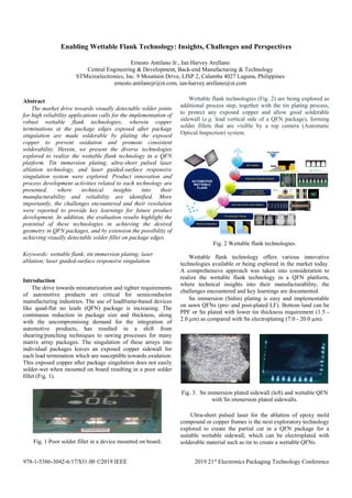
  • 1. 978-1-5386-3042-6/17/$31.00 ©2019 IEEE 2019 21st Electronics Packaging Technology Conference Tin Immersion Plating O Ultra Short Pulse Laser Ablation B Laser guided-surface Responsive Singulation U Solderable Wettable Sidewall S AOI Capable T Top Camera Standard Singulation R AUTOMOTIVE WETTABLE FLANK Enabling Wettable Flank Technology: Insights, Challenges and Perspectives Ernesto Antilano Jr., Ian Harvey Arellano Central Engineering & Development, Back-end Manufacturing & Technology STMicroelectronics, Inc. 9 Mountain Drive, LISP 2, Calamba 4027 Laguna, Philippines ernesto.antilanojr@st.com, ian-harvey.arellano@st.com Abstract The market drive towards visually detectable solder joints for high reliability applications calls for the implementation of robust wettable flank technologies, wherein copper terminations at the package edges exposed after package singulation are made solderable by plating the exposed copper to prevent oxidation and promote consistent solderability. Herein, we present the diverse technologies explored to realize the wettable flank technology in a QFN platform. Tin immersion plating, ultra-short pulsed laser ablation technology, and laser guided-surface responsive singulation system were explored. Product innovation and process development activities related to each technology are presented, where technical insights into their manufacturability and reliability are identified. More importantly, the challenges encountered and their resolution were reported to provide key learnings for future product development. In addition, the evaluation results highlight the potential of these technologies in achieving the desired geometry in QFN packages, and by extension the possibility of achieving visually detectable solder fillet on package edges. Keywords: wettable flank; tin immersion plating; laser ablation; laser guided-surface responsive singulation Introduction The drive towards miniaturization and tighter requirements of automotive products are critical for semiconductor manufacturing industries. The use of leadframe-based devices like quad-flat no leads (QFN) package is increasing. The continuous reduction in package size and thickness, along with the uncompromising demand for the integration of automotive products, has resulted in a shift from shearing/punching techniques to sawing processes for many matrix array packages. The singulation of these arrays into individual packages leaves an exposed copper sidewall for each lead termination which are susceptible towards oxidation. This exposed copper after package singulation does not easily solder-wet when mounted on board resulting in a poor solder fillet (Fig. 1). Fig. 1 Poor solder fillet in a device mounted on board. Wettable flank technologies (Fig. 2) are being explored as additional process step, together with the tin plating process, to protect any exposed copper and allow good solderable sidewall (e.g. lead vertical side of a QFN package), forming solder fillets that are visible by a top camera (Automatic Optical Inspection) system. Fig. 2 Wettable flank technologies. Wettable flank technology offers various innovative technologies available or being explored in the market today. A comprehensive approach was taken into consideration to realize the wettable flank technology in a QFN platform, where technical insights into their manufacturability, the challenges encountered and key learnings are documented. Sn immersion (SnIm) plating is easy and implementable on sawn QFNs (pre- and post-plated LF). Bottom land can be PPF or Sn plated with lower tin thickness requirement (1.5 - 2.0 µm) as compared with Sn electroplating (7.0 - 20.0 µm). Fig. 3. Sn immersion plated sidewall (left) and wettable QFN with Sn immersion plated sidewalls. Ultra-short pulsed laser for the ablation of epoxy mold compound or copper frames is the next exploratory technology explored to create the partial cut in a QFN package for a suitable wettable sidewall, which can be electroplated with solderable material such as tin to create a wettable QFNs. 595
  • 2. 2019 21st Electronics Packaging Technology Conference Laser guided-surface responsive singulation system is a wafer dicing technology benchmarked for pioneering strategy to overcome inherent package constraints such as tolerance of half etch location and width, tolerance of blade thickness, machine tolerance for blade path alignment, strip camber, coil set and crossbow maximum specification, machine chuck table planarity, and strip warpage in achieving a step-cut package profile. The solution takes advantage of a laser surface detection (LSD) module able to map the surface contour, and feedback the data to adjust the cutting depth, resulting in a consistent cut depth regardless of the strip warpage level. Methodology QFN packages with wettable sidewalls were produced using several technologies namely, SnIm plating, ultra-short pulsed laser for the ablation of epoxy mold compound or copper frames, and laser guided-surface responsive singulation system. SnIm plating process was accomplished on standard QFN packages following the process flow shown in Figure 4. SnIm is introduced after the exposition of the sidewalls by the singulation process. The process starts with a degreasing step, aiming at the removal of organic contaminants on the sidewall surface, possibly introduced during the singulation process, or during the staging time. A micro-etching step prepares the Cu surface by removing surface oxides, and reducing roughness imparted by the singulation process. The actual plating process starts with a pre-dip process. This step is designed to develop a very thin layer of Sn, reducing the mismatch between the actual Sn layer grown during the main plating step, and the Cu layer. The main plating step is where the deposition of 0.5 - 2.5 μm of Sn occurs. Afterwhich, a postdip process could be introduced to increase the corrosion resistance of the plated layer. Several rinsing steps are present in between process steps to prevent cross contamination of the chemical baths, and the removal of residual chemical that can affect the integrity of the overall product. Hot drying is the final step, aimed at removing any traces of solution that can induce corrosion during storage. For the ultra-short pulsed laser for the ablation of epoxy mold compound or copper frames technology, Standard QFN package was assembled using standard process involving the attachment of a semiconductor die onto a copper leadframe using a die attach material, electrically connecting the die to the leadframe using a thin metal wire, and encapsulating the package using an epoxy molding compound. The partial cut was realized using a commercially available laser system with a wavelength of 1030 nm, an average power of 40 W, frequency range of 200 - 800 kHz, beam quality M2 of less than 1.3, pulse energy of less than 200 μJ and pulse width of 800 ± 200 fs. In the case of the laser guided-surface responsive singulation system, standard QFN package was assembled using standard process involving the attachment of a semiconductor die onto a copper leadframe using a die attach material, electrically connecting the die to the leadframe using a thin wire, and encapsulating the package using an epoxy molding compound. The partial- and full-cut were realized using a commercially available DFD6362HC (NLA219) DISCO Fully Automatic Dicing Saw with laser surface detection (LSD) feature. The electroplating process was performed using Stannopure 100 plating chemistry from Atotech. Pre-Assembly Diebond Wirebond Molding Marking Singulation Test & Finish Tin Immersion VMI Loading Degreasing Micro Etch Rinse Pre Dip Sn Immersion Rinse Rinse Hot Air Dry Unloading Rinse Post Dip Fig. 4. Sn immersion process flow. Results and Discussion SnIm Plating. The feasibility of SnIm plating process as a solution to the wettable flank challenge has been rigorously evaluated. Process parameters have been optimized based on several criteria, designed to assess the mechanical integrity, and reliability of the plated area. During the course of the evaluation, several defect signatures have been repeatedly encountered. This report summarizes the defect manifestations, and presents the insights into the origin of these plating defects. Exposed Cu. This defect has been observed during the initial stages of the SnIm process evaluation. Unsuccessful plating of the sidewall (Fig. 5), in entirety or portions thereof, is due to the presence of contaminants on the Cu surface. The presence of this defect is an indication of the ineffective degreasing or micro-etch steps. In the SnIm process, the reduction and deposition of Sn on the sidewall is coupled with the oxidation of Cu, occurring via a redox shuttle. In the presence of contaminants such as organic materials coming from adhesives or the molding compound, the Cu layer is blocked, impeding the deposition and growth of Sn. It can also be observed that the exposed surface is generally rough, possibly due to the anisotropic etching of the surface during micro-etching and/or uncontrolled deposition within the contaminant pores, where the Cu underlayer is exposed. 596
  • 3. 2019 21st Electronics Packaging Technology Conference Fig. 5 Exposed Cu manifestations after SnIm plating. Porosity. This defect is one of the most prevalent, occurring predominantly along the edges (Fig. 6). The porous structure originates from the expulsion of bubbles from the surface. These bubbles originate from dissolved gases due to the solution turnover, a process necessary to keep the homogeneity of the chemistry. Minimizing the turnover resulted in a smoother surface morphology with minimal porosity. Porosity was also observed during the evaluation of a modified chemistry. The chemistry supplier incorporated a proprietary surfactant, designed to reduce the surface energy thereby increasing the efficacy of the Sn deposition. However, the surfactant concentration in solution is high enough to cause severe frothing, leading us to speculate that the critical micelle concentration was reached. In this case, the surfactant molecules form micelles with trapped air in the core. The resulting SnIm deposit is uncharacteristically rough, with very high degree of porosity due to the expulsion of large quantities of trapped air. Fig. 6 Porosity manifestations after SnIm plating. Whiskers. Compressive mechanical stresses induce whisker growth. Sources of these stresses include residual stresses from the plating process, mechanically induced stresses, stresses by intermetallic and/or oxide layer growth, and thermal stresses. Initially, whisker growth in SnIm is considered low risk as compared with electroplated Sn because of the large grain size which is the same order of magnitude as the layer thickness. However, the layer thickness of SnIm has low mechanical stress dissipative capacity and IMCs form almost spontaneously upon deposition, both of which promote whisker growth. The growth is confirmed in samples stored under N2 atmosphere for 12-14 months. Fig. 7 shows various configurations of SnIm whiskers with lengths up to 240 μm, and density of 1.1 x 10⁻⁴ whiskers/μm2 . These results support previous findings, 13-14 highlighting the susceptibility of SnIm plating to whiskers growth. Mechanistically, these growths could be related to the thickness (<3.0 μm) which is below the iNEMI recommendation of 8 μm15, having less efficient dissipation of mechanical stress, and high degree of residual stress due to the mismatch of Cu and Sn. In addition, the fast IMC formation leads to higher IMC fractions in SnIm as compared with electroplated Sn at any given time, further reducing the thickness of the pure Sn layer. Fig. 7 Sn whiskers after 12-14 months under an N2 environment. Ultra-short pulsed laser for the ablation of epoxy mold compound or copper frames technology. Laser ablation is a mature and robust technology utilized in several scientific, technological and industrial processes. The process utilizes a laser beam focused on a sample surface to remove material from the irradiated zone. Materials absorbing the laser energy could be evaporated or sublimated (low flux), or could be converted to plasma (high flux). The tremendous advances in laser technology has basically produced versatile laser ablation processes by providing lasers with varying power, flux, pulsed rates and other customized features. Laser ablation process using ultra-short pulsed laser was explored to achieve a step-cut package design by demonstrating laser ablation in epoxy mold compound (EMC) and copper frames in QFN packages (Fig. 8). By utilizing a lead design that is partially offset from the package outline edge (e.g. pull-back leads or partially etched), it is possible to achieve a partial-cut package configuration. 597
  • 4. 2019 21st Electronics Packaging Technology Conference Fig. 8 Laser ablation of EMC resulting in step-cut configuration. Fig. 9 Laser ablation of Cu frame with a-b) wide trench and c) two parallel narrow trenches resulting in step-cut configuration. b) Tilted view showing sidewalls with no heat affected zone (HAZ). During the QFN assembly process, the leadframe recesses are filled at the molding process. The cured EMC is then removed via laser ablation resulting in the exposition of the flank on leads. Residual resins and fillers were successfully removed using chemical deflash and high pressure water jet. Results clearly show that laser ablation of EMC is a promising strategy to realize step-cut QFN configuration. It is also possible that instead of removing the EMC, the cut is made via laser ablation of the Cu frame. By using a laser with a lasing capacity enough to vaporize Cu material, standard QFN frame design, i.e., no pull-back leads, could be used to achieve the same result. In this case, wide trench cut or two parallel narrow trench cuts could be made to expose the flank on leads (Fig. 9). The latter was explored to improve the cycle time of the process, wherein instead of cutting through the entire width of the saw lane, narrow trenches enough to expose the sidewalls are made. Nonetheless, both cutting configurations successfully achieved the step-cut geometry of the package. Moreover, no heat affected zones (HAZ) were observed due to the ultra-short laser pulses used in these evaluations. These results highlight the potential of laser ablation of Cu frames in achieving the desired geometry in QFN packages, and by extension the possibility of achieving visually detectable solder fillet on package edges. Laser guided-surface responsive singulation system. The technology takes advantage of a Laser Surface Detection (LSD) module able to map the surface contour, and feedback the data to adjust the cutting depth, resulting in a consistent cut depth regardless of the strip warpage level. Achieving a step-cut package profile using conventional singulation process is a challenge due to its inherent susceptibility towards inconsistent cut depth and over cutting, primarily due to the variability in the surface height because of the strip warpage. Fig. 10 shows the inconsistent and wide range of cut depth achieved using conventional singulation process, which does not satisfy the package requirement. This prompted the group to explore alternative systems that could lead to a more consistent cut depth. Capitalizing on the robust wafer step-cut singulation process, coupled with an innovative laser guided- Fig. 10 Laser ablation of EMC resulting in step-cut configuration. Fig. 11 Laser surface detection-assisted singulation process. 598
  • 5. 2019 21st Electronics Packaging Technology Conference surface responsive module (Fig. 11), we evaluated the viability of transferring the wafer dicing process into the package level singulation process. The primary challenge is to overcome the large variability in strip warpage along the length and width of the leadframe (Fig. 12), which can be accurately measured by the LSD module. The surface contour detected by the LSD module is used as an input parameter to adjust the blade height resulting in a tighter and consistent cut depth (Fig. 13). More importantly, the cut depth profile and morphology (Fig. 14) satisfy the requirements of the succeeding critical processes. Fig. 12 Laser surface detection-assisted singulation process. Fig. 13 Cut depth consistency along length (left) and width (right) of the LF. Initial evaluation and revalidation runs for two package requirement cut depth (Fig 15) consistently surpassed expectations, making the laser guided-surface responsive singulation system a viable solution towards achieving the step-cut package profile requirement. The introduction of LSD with wafer dicing accuracy to package-level singulation proved to be a robust solution to maintain consistent multilayered cutting depth, satisfying complex thin semiconductor technology. Fig. 14 Cut depth profile and morphology. Fig. 15 Cut depth results from the initial evaluation (left) and the revalidation (right). The step-cut created by the LSD singulation system is made solderable via standard Sn electroplating process, where 50 ± 5% of the lead sidewall is plated with Sn. Mounting the device on board created a solder fillets that are visually detectable via standard AOI systems. 599
  • 6. 2019 21st Electronics Packaging Technology Conference Conclusion Several technologies were explored to realize the wettable flank in a QFN platform, resulting in the AOI-detectable solder fillets. The defect signatures encountered during the qualification of the SnIm plating process demonstrated that SnIm layer is not technologically limiting primarily due to the thin layer, which is way below the iNEMI recommended thickness. These results lead the team to conclude that SnIm process is not suitable to create the wettable flank, considering the high reliability requirement of the automotive industry. Laser ablation of epoxy molding compound or Cu frame was successfully attained using ultra-short pulsed laser technology. The partial cut geometry achieved in this process brick enables the exposition of the sidewall, which could be plated to create a wettable sidewall, thereby satisfying the customer requirement for visually detectable solder joints for high reliability applications. However, some manufacturability concerns were encountered primarily due to incomplete removal of silica fillers from the EMC, resulting in some solderability problems. As a result of the evaluation and revalidation studies, LSD provides a solution for a consistent multilayered cutting steps. The accurate control of this technology enabled the production of highly controlled step cut configuration, which when electroplated with Sn layer results in consistently solderable sidewall surface. This technology is the program of reference in attaining the AOI-detectable solder fillet in a QFN platform. Acknowledgments The authors thank the whole NPD&I and Assembly Operations Team for the support during the course of evaluation. The management support of STM CALAMBA is rightfully acknowledged. References 1. Chuang, C.L., Aoh, J.N., Din, R.F. Oxidation of copper pads and its influence on the quality of Au/Cu bonds during thermosonic wire bonding process. Microelectron. Reliab. 2006, 46, 449-458. 2. Berthold, T., Benstetter, G., Frammelsberger, W., Rodriguez, R., Nafria, M. Nanoscale characterization of copper oxide films by Kelvin Probe Force Microscop. Thin Solid Films, 2015, 584, 310-315. 3. Ganjei, J. Improved QFN Reliability by flank tin plating process after singulation. Microsystems, Packaging, Assembly and Circuits Technology Conference (IMPACT), 2015 10th International, Taipei, 2015, 137- 140. 4. Barthelmes, J., Kok, S. W., Neoh, D. G., Kurtz, O. Highly efficient corrosion protection for plated pure tin surfaces. Electronic Manufacturing Technology Symposium (IEMT), 2008 33rd IEEE/CPMT International, Penang, 2008, 1-4. 5. Özkök, M., Mertens, H., Bender, J., Bruder, M. Forming solder filet on leadframe edges of a QFN with immersion tin. Electronics Packaging Technology Conference (EPTC 2013), 2013 IEEE 15th, Singapore, 2013, 677- 680. 6. Cadot, G.B.J., Axinte, D.A., Billingham, J. Continuous trench, pulsed laser ablation for micro-machining applications. Int. J. Mach. Tool Manu. 2016, 107, 8-20. 7. Dubey, A.K., Yadava, V. Laser beam machining-A review. Int. J. Mach. Tool Manu. 2008, 48, 609-628. 8. Hernandez, E., Alfano, M. Lubineau, G. Buttner, U. Improving adhesion of copper/epoxy joints by pulsed laser ablation. Int. J. Adhes. Adhes., 2016, 64, 23-32. 9. Li, C.-H., Tsai, M.-J., Yang, C.-D. Study of optimal laser parameters for cutting QFN packages by Taguchi's matrix method. Optics Laser Technol., 2007, 39, 786-795. 10. Sartinska, L.L., Barchikovski, S., Wagenda, N., Rud, B.M., Timofeeva, I.I. Laser induced modification of surface structures. Appl. Surf. Sci., 2007, 253, 4295-4299. About the Authors Ian Harvey J. Arellano, Ph.D. is a Senior Staff Engineer at the New Product Introduction Department at STMicroelectronics, Inc. leading new materials and chemical-based processes development. He received his Ph.D. in Applied Science (Chemistry) from the University of South Australia, and Master and Bachelor of Science in Chemistry from the University of the Philippines- Diliman. He has seven years of experience in the academe teaching Chemistry and Materials Science courses to undergraduate and graduate students, and seven years of experience in the semiconductor industry. Ernesto ANTILANO Jr. is a Senior Process Engineer at Back-end Manufacturing & Technology Central Engineering & Development at STMicroelectronics, Inc. leading Mold process development. He has Twenty-two years of experience in the industry and gained his first semiconductor experience at Team Pacific Corporation as FOL wirebond technician. A graduate of Technological University of the Philippines–Visayas with a degree of Electronics Technology and soon a graduate of Technological University of the Philippines Taguig with a bachelor’s degree in Electronics and Communication Engineer. 600