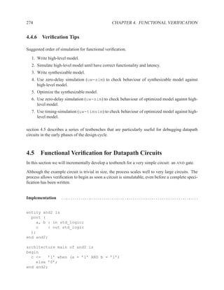
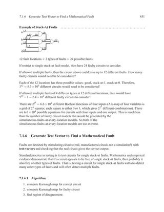
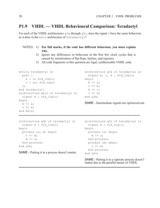
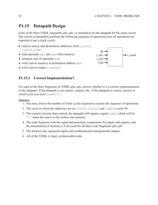
Downloaded 268 times


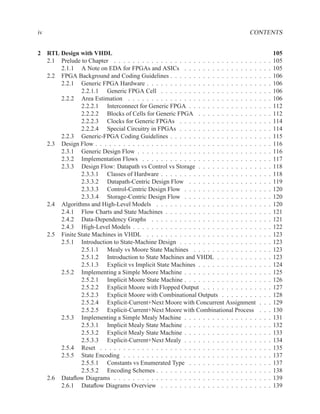
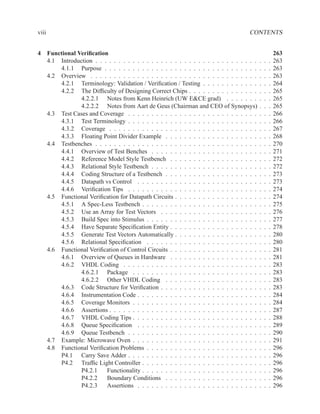

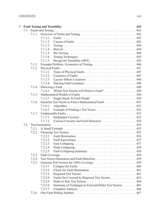


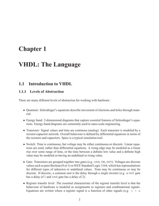

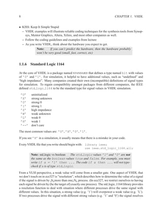


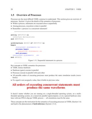
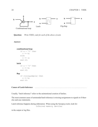
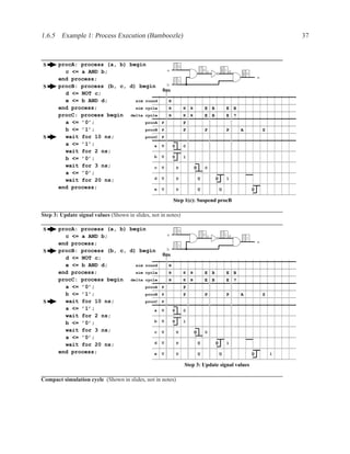
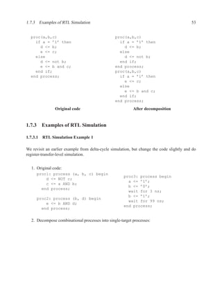
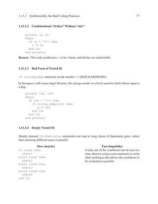
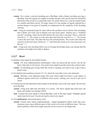
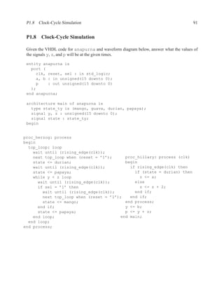
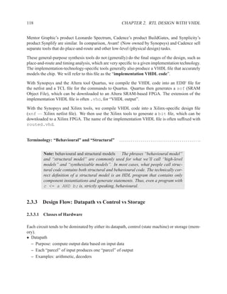
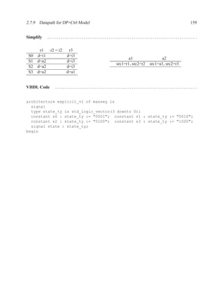
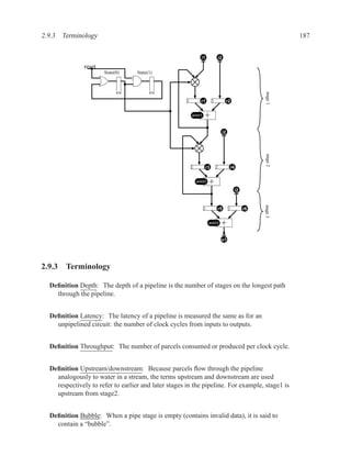
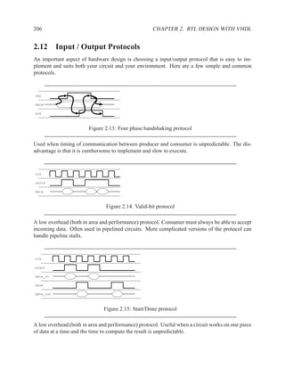
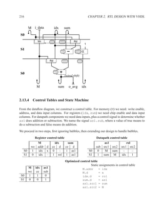
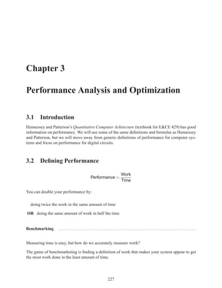
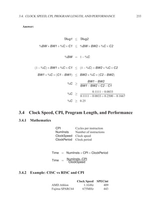
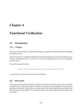
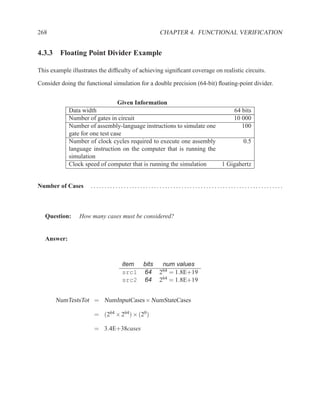
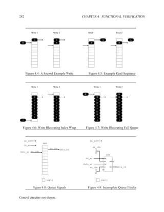
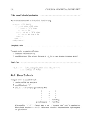
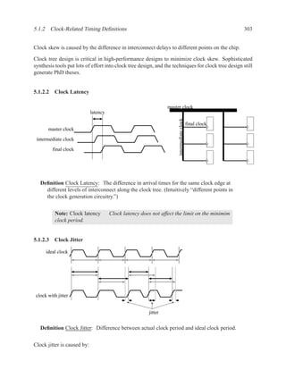
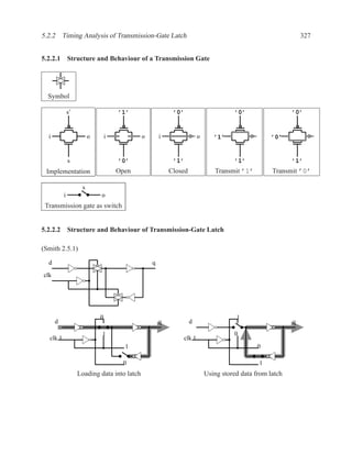
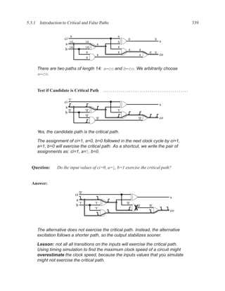
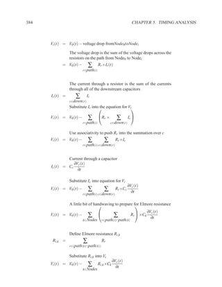
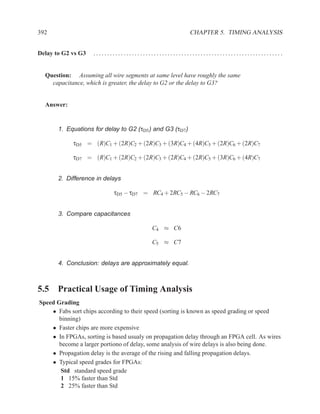
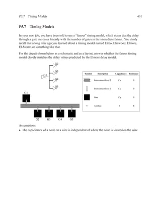
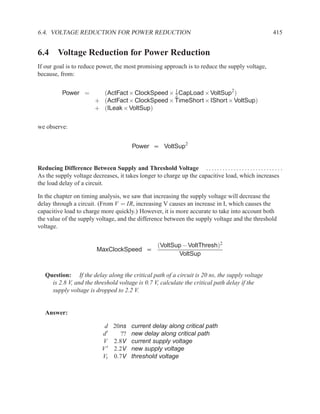
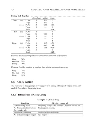
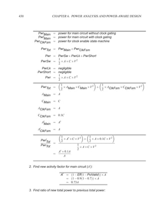
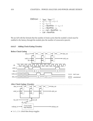
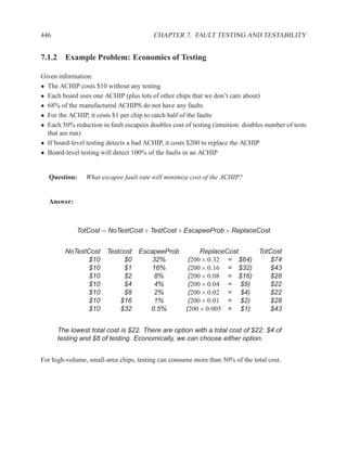
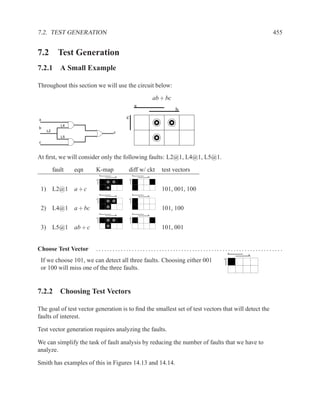
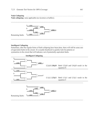
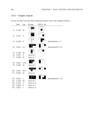
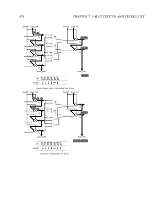
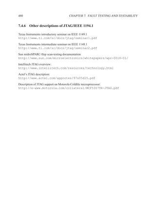
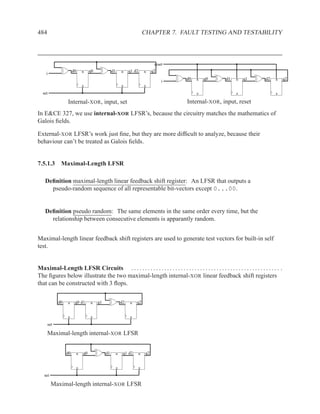
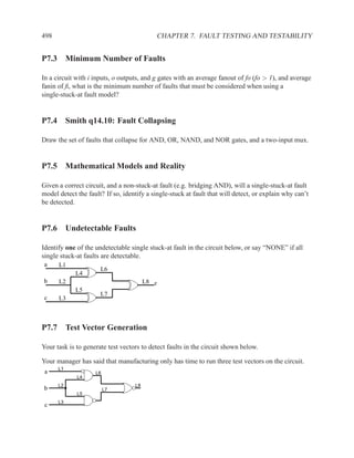
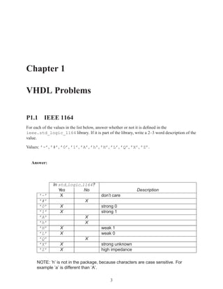
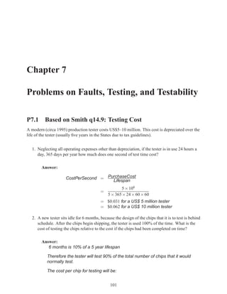
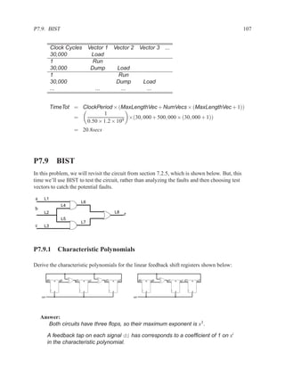
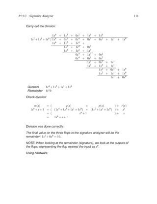
![1.3.3 Entities and Architecture 13
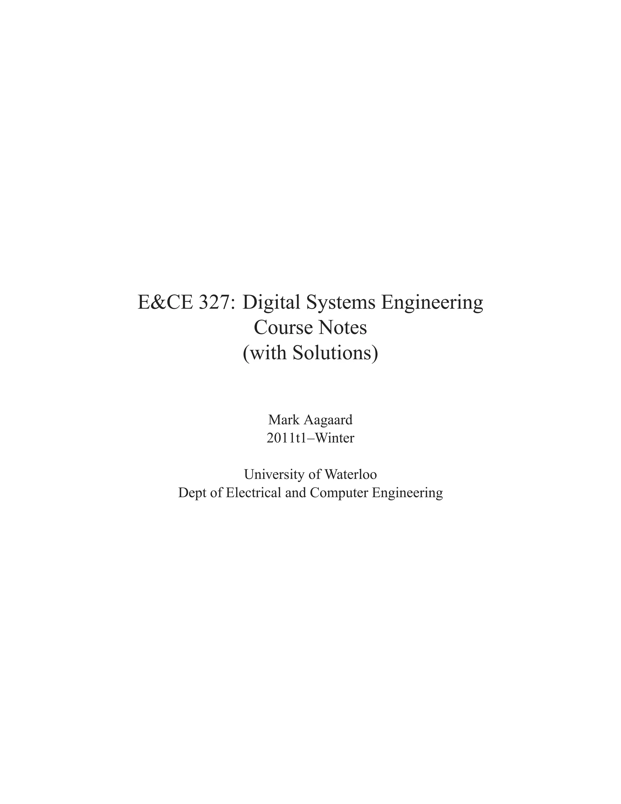
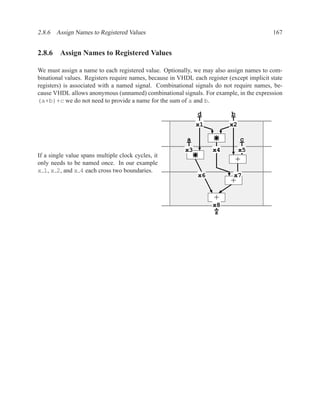
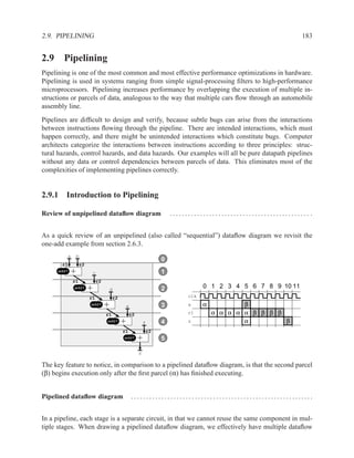
The syntax of VHDL is defined using a variation on Backus-Naur forms (BNF).
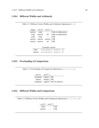
[ { use_clause } ]
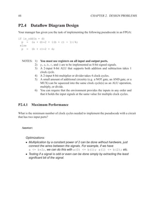
entity ENTITYID is
[ port (
{ SIGNALID : (in | out) TYPEID [ := expr ] ; }
);
]
[ { declaration } ]
[ begin
{ concurrent_statement } ]
end [ entity ] ENTITYID ;
Figure 1.3: Simplified grammar of entity
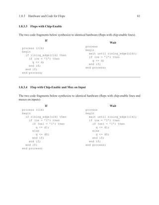
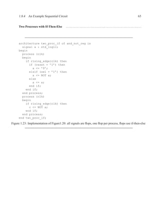
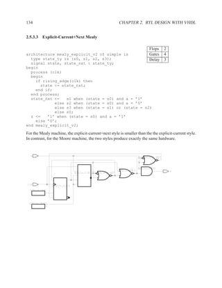
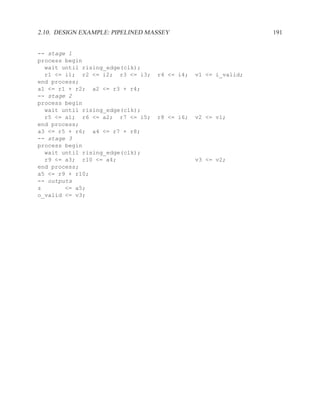
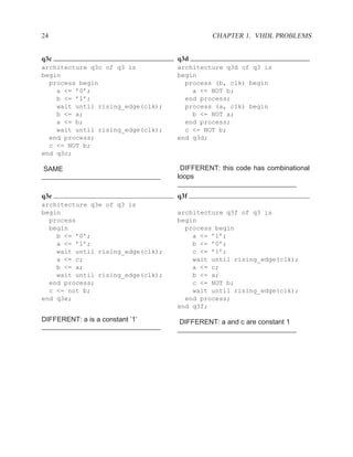
architecture main of and_or is
signal x : std_logic;
begin
x <= a AND b;
z <= x OR (a AND c);
end main;
Figure 1.4: Example of architecture
[ { use_clause } ]
architecture ARCHID of ENTITYID is
[ { declaration } ]
begin
[ { concurrent_statement } ]
end [ architecture ] ARCHID ;
Figure 1.5: Simplified grammar of architecture](https://image.slidesharecdn.com/vhdlreference-111231052552-phpapp02/85/VHDL-Reference-35-320.jpg)
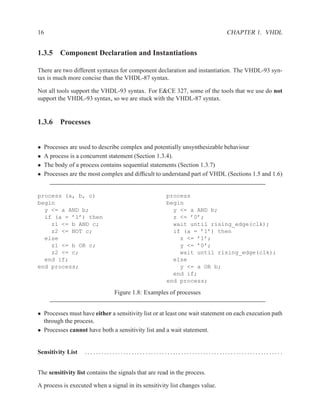
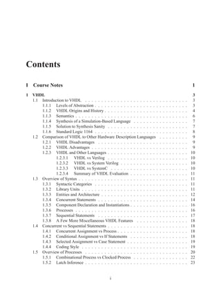
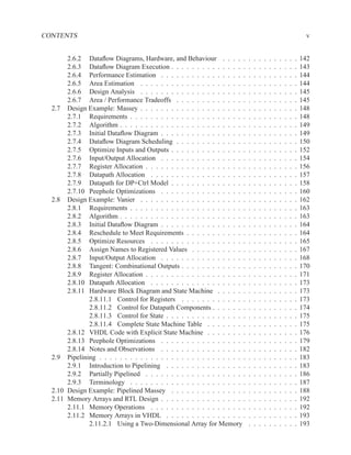
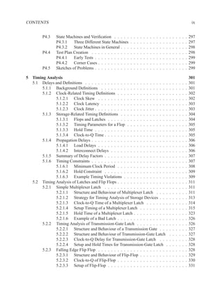
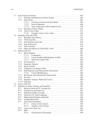
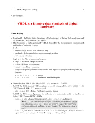
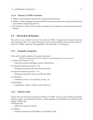
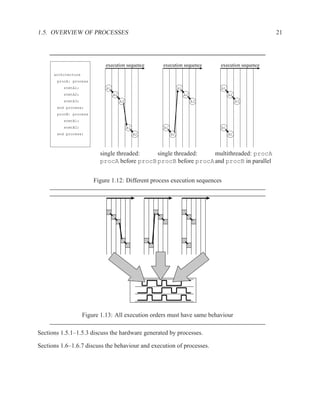
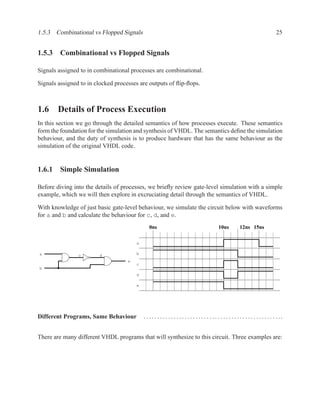
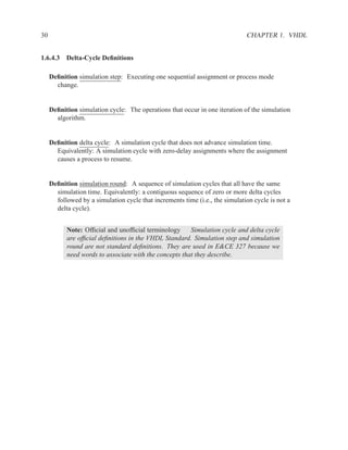
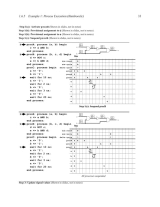
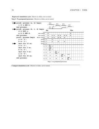
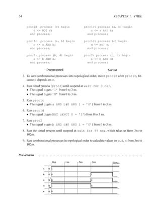
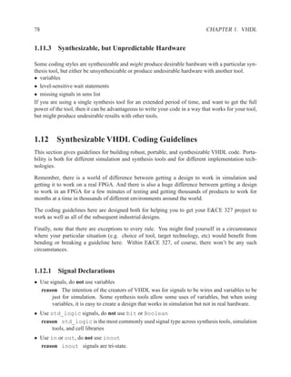
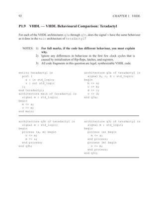
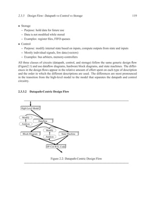
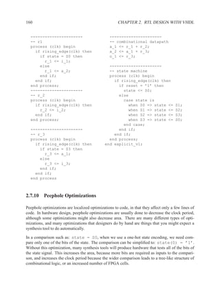
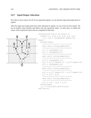
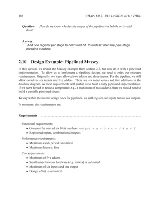
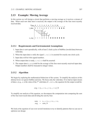
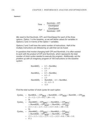
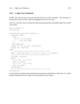
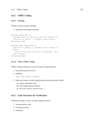
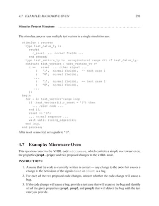
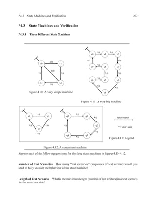
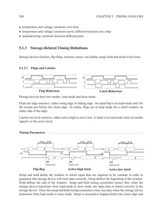
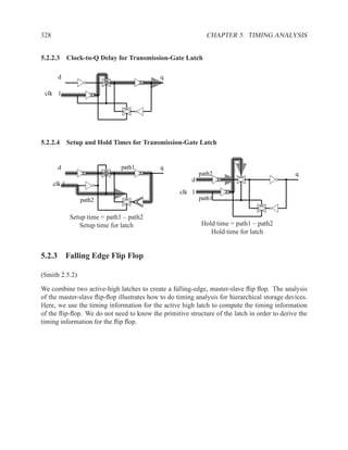
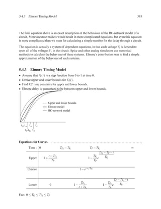
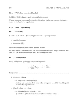
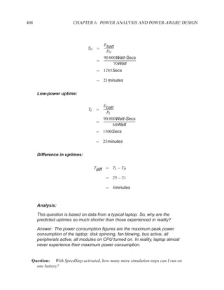
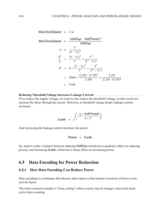
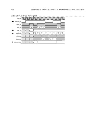
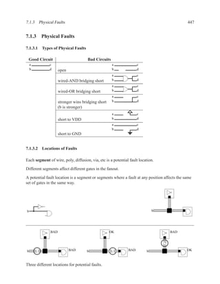
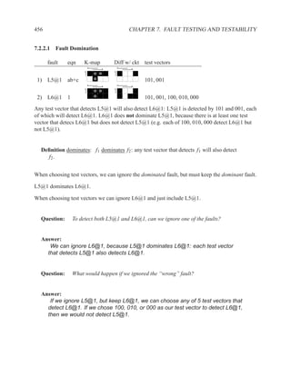
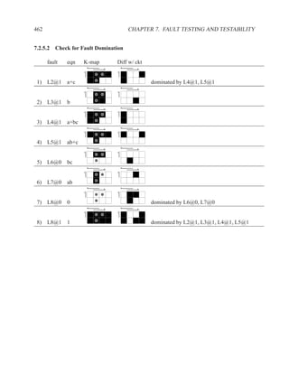
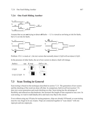
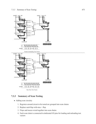
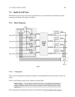
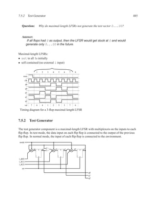
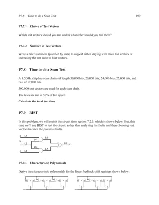
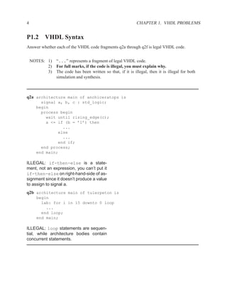
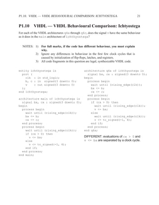
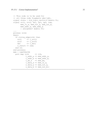
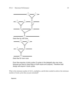
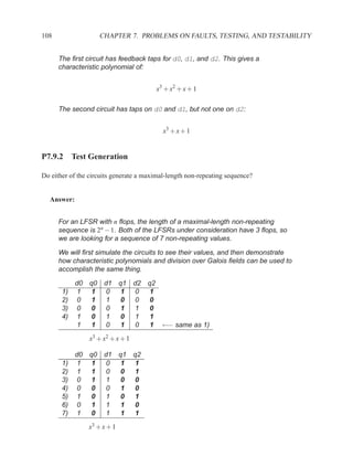
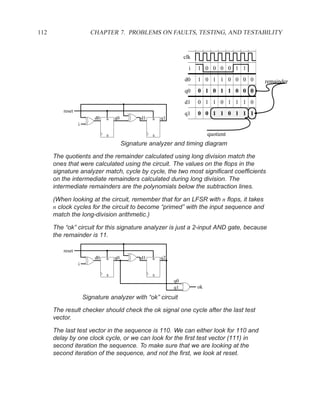
![1.3.7 Sequential Statements 17
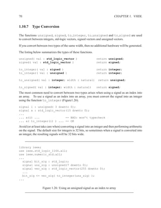
An important coding guideline to ensure consistent synthesis and simulation results is to include
all signals that are read in the sensitivity list. If you forget some signals, you will either end up
with unpredictable hardware and simulation results (different results from different programs) or
undesirable hardware (latches where you expected purely combinational hardware). For more on
this topic, see sections 1.5.2 and 1.6.
There is one exception to this rule: for a process that implements a flip-flop with an if rising edge
statement, it is acceptable to include only the clock signal in the sensitivity list — other signals
may be included, but are not needed.
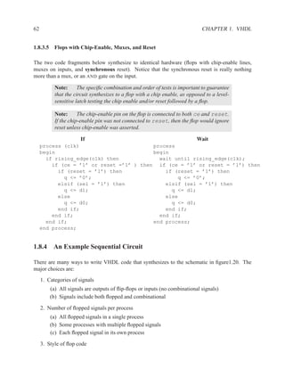
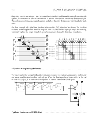
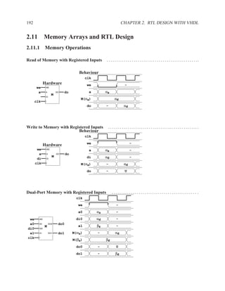
[ PROCLAB : ] process ( sensitivity_list )
[ { declaration } ]
begin
{ sequential_statement }
end process [ PROCLAB ] ;
Figure 1.9: Simplified grammar of process
1.3.7 Sequential Statements
Used inside processes and functions.
wait wait until . . . ;
signal assignment . . . <= . . . ;
if-then-else if . . . then . . . elsif . . . end if;
case case . . . is
when . . . | . . . => . . . ;
when . . . => . . . ;
end case;
loop loop . . . end loop;
while loop while . . . loop . . . end loop;
for loop for . . . in . . . loop . . . end loop;
next next . . . ;
Figure 1.10: The most commonly used sequential statements](https://image.slidesharecdn.com/vhdlreference-111231052552-phpapp02/85/VHDL-Reference-39-320.jpg)
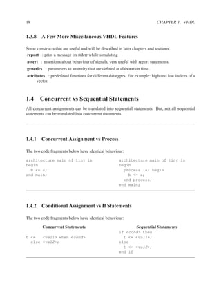
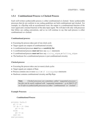
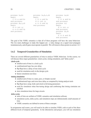

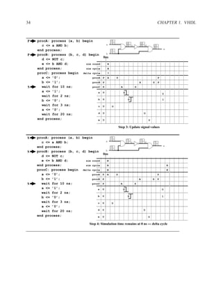
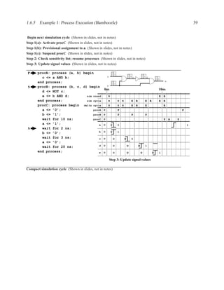
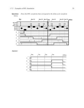
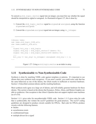
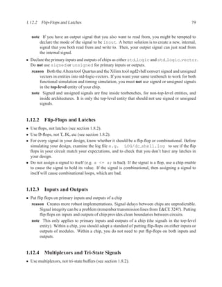
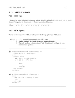


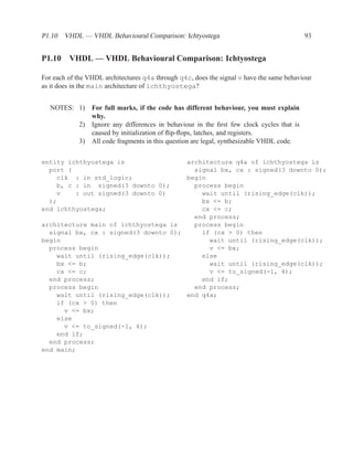

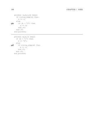
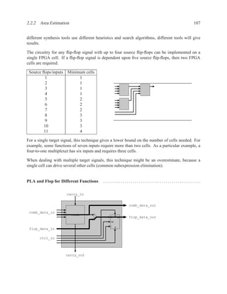


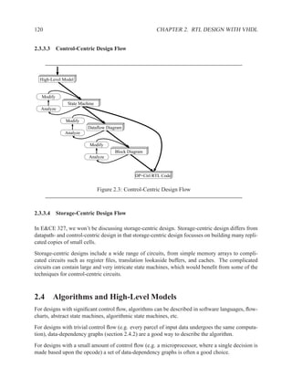

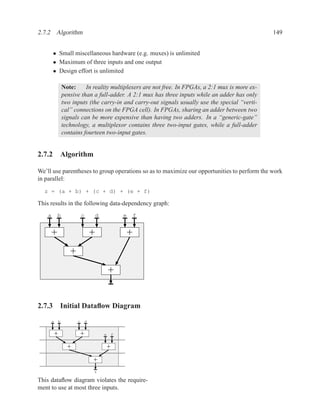
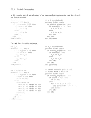
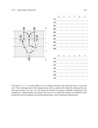
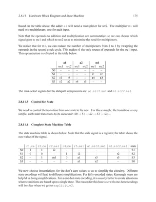
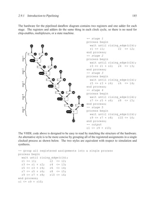
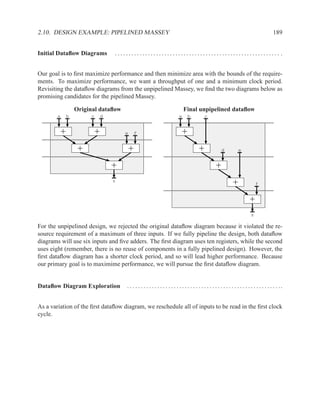
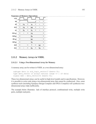
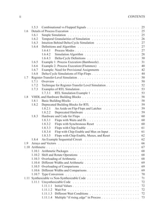
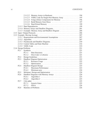
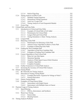
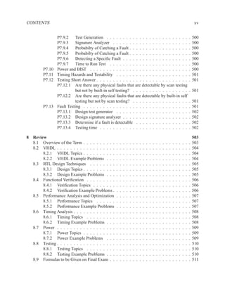
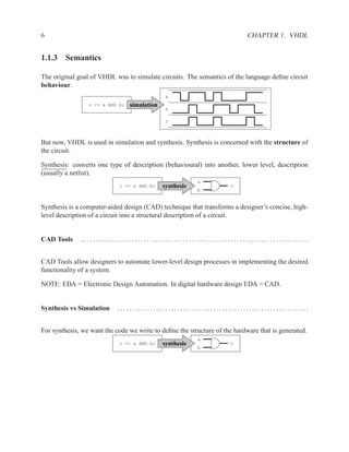
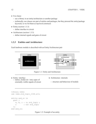
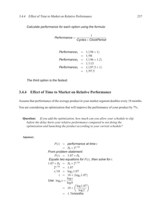
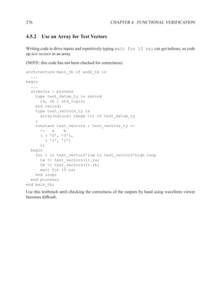
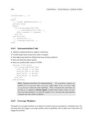
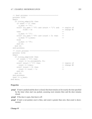
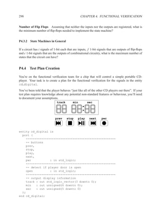
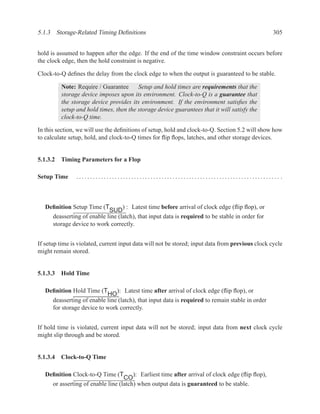
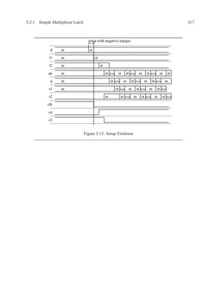
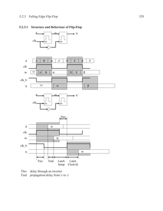
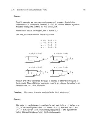
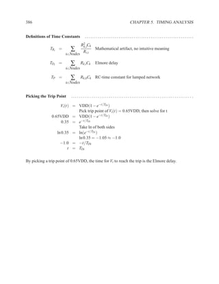
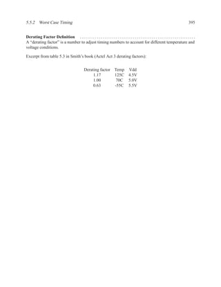
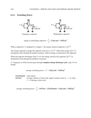
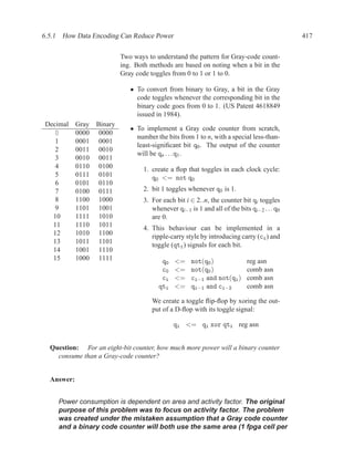
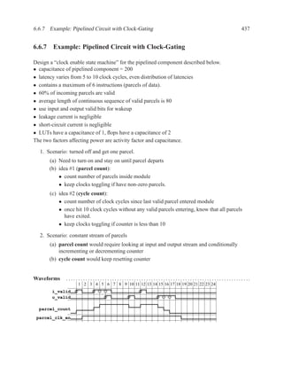
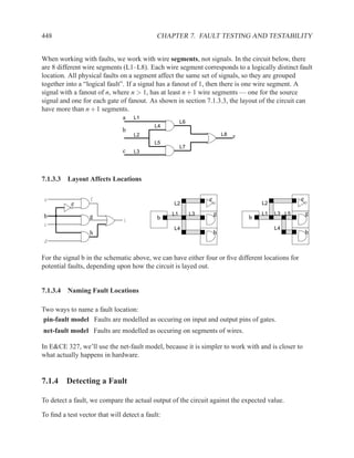
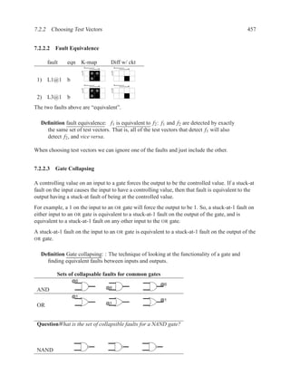
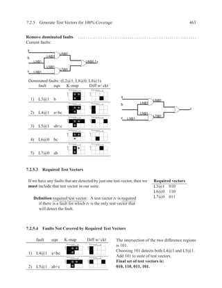
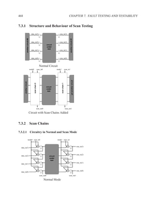
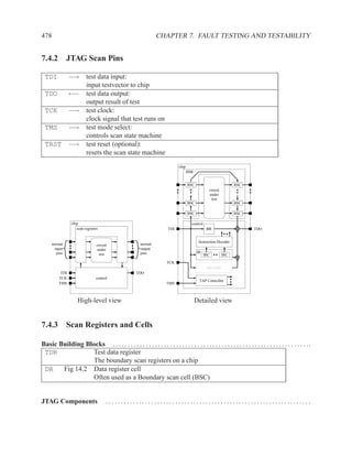
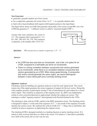
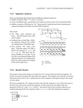
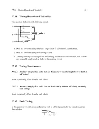
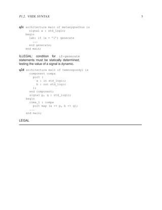
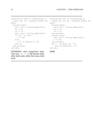
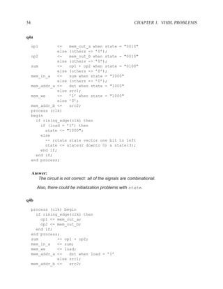
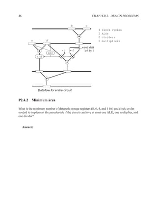
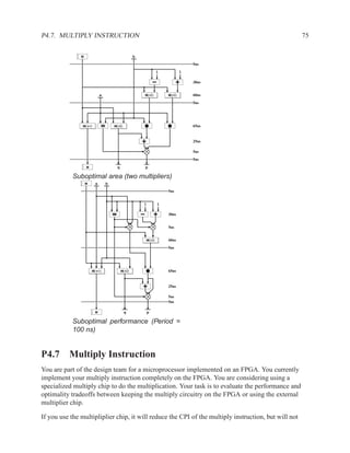
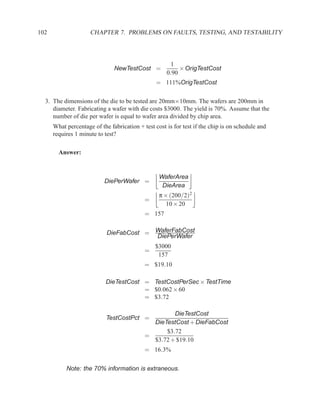
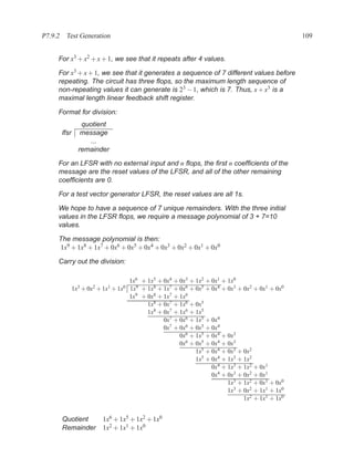
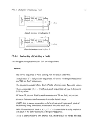
![2.11.2 Memory Arrays in VHDL 197
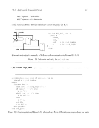
2.11.2.5 Build Memory from Slices
If the vendor’s libraries of memory components do not include one that is the correct size for your
needs, you can construct your own component from smaller ones.
WriteEn
Addr
DataIn[W-1..0]
DataIn[2W-1..2]
Clk
WE WE
A DO A DO
DI NxW DI NxW
DataOut[W-1..0]
DataOut[2W-1..W]
Figure 2.7: An N×2W memory from N×W components
WriteEn
WE
Addr[logN]
Addr[logN-1..0] A DO
DataIn DI NxW
Clk
WE
A DO
DI NxW
0 1
DataOut
Figure 2.8: A 2N×W memory from N×W components](https://image.slidesharecdn.com/vhdlreference-111231052552-phpapp02/85/VHDL-Reference-219-320.jpg)
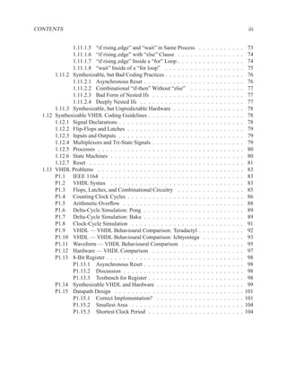
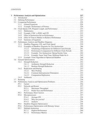
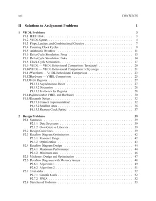
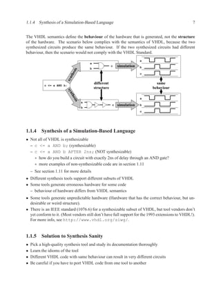
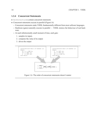
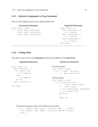
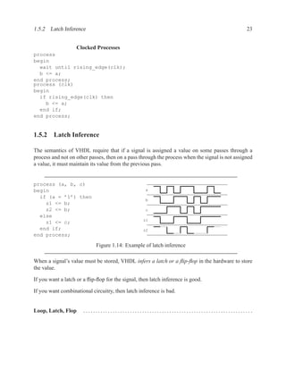
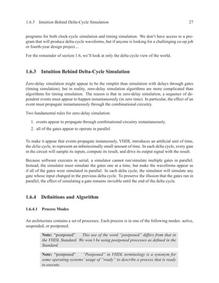
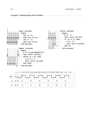
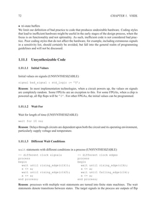
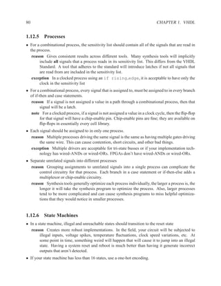
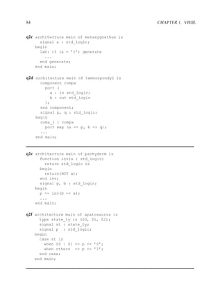
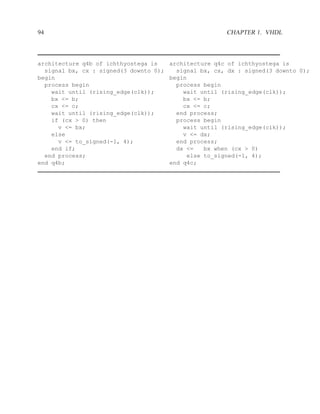
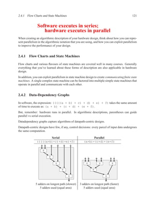
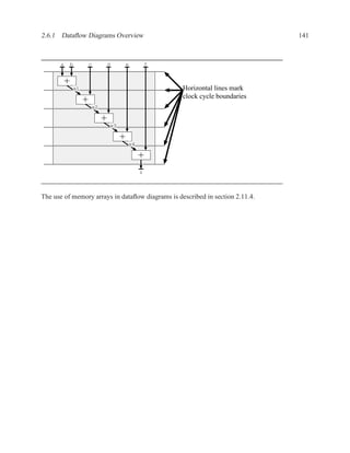
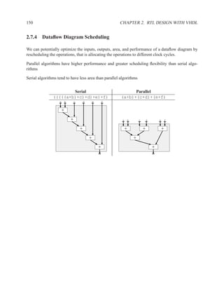
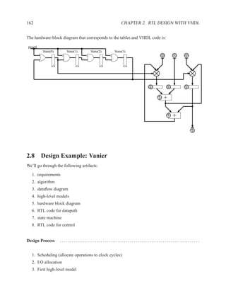
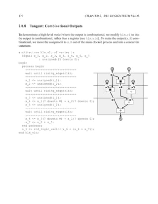
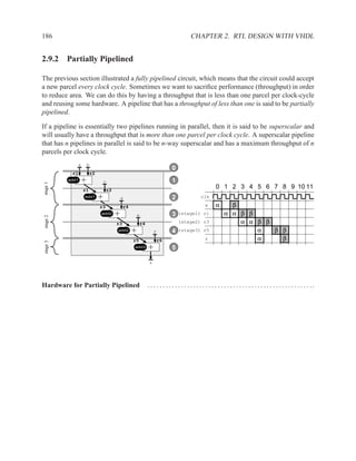
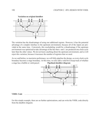
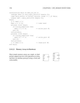
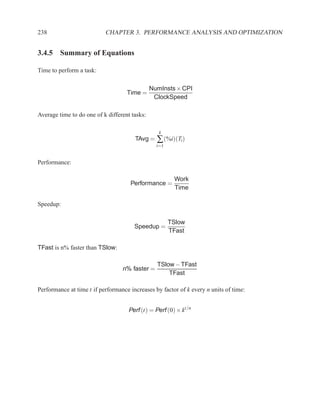
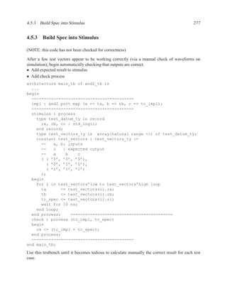
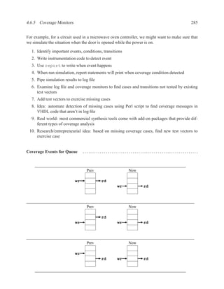
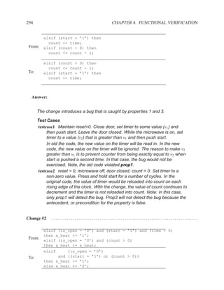
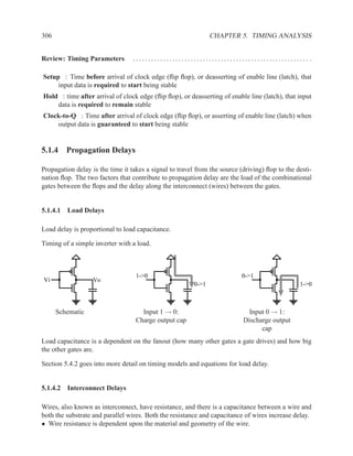
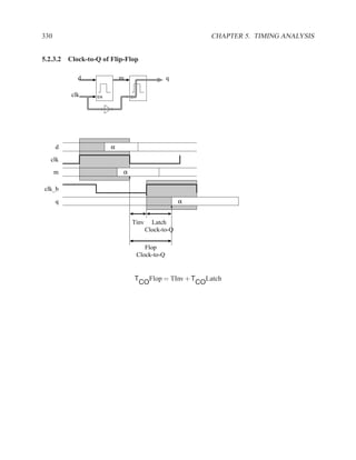
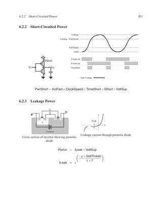
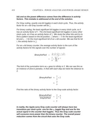
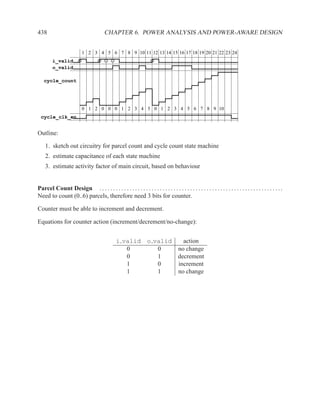
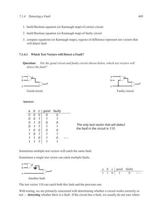
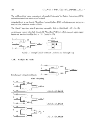
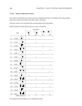
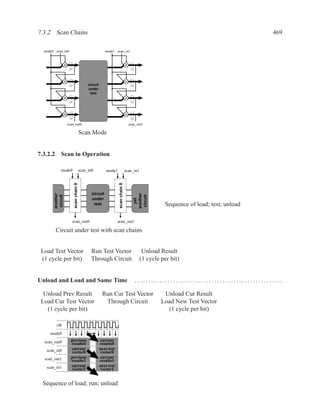
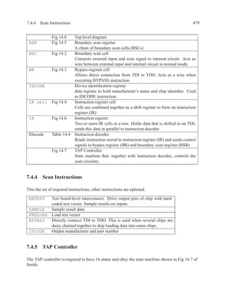
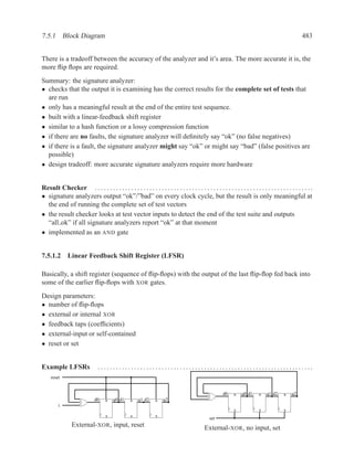
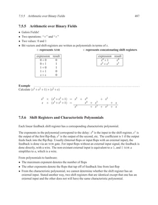
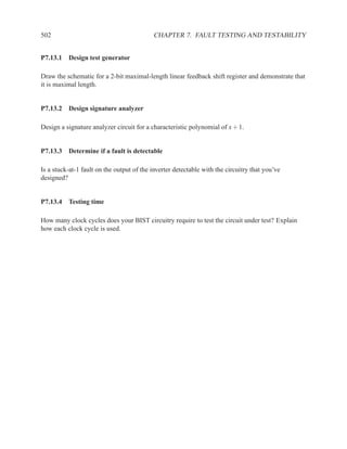
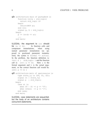
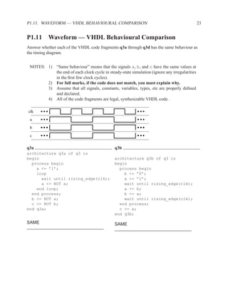
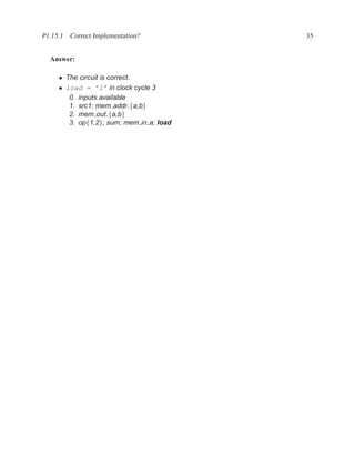
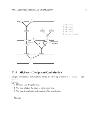
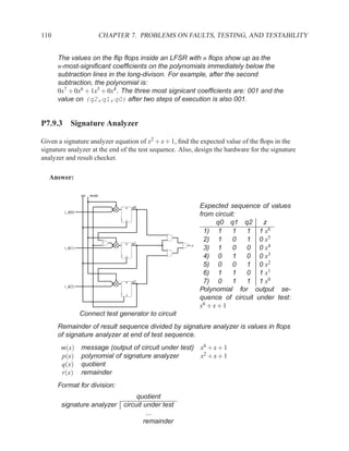
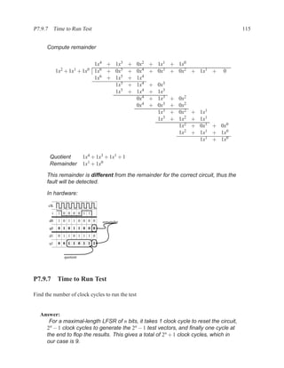
![2.11.3 Data Dependencies 199
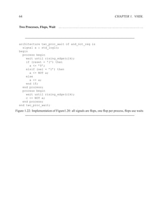
2.11.2.6 Dual-Ported Memory
Dual ported memory is similar to single ported memory, except that it allows two simultaneous
reads, or a simultaneous read and write.
When doing a simultaneous read and write to the same address, the read will usually not see the
data currently being written.
Question: Why do dual-ported memories usually not support writes on both ports?
Answer:
What should your memory do if you write different values to the same
address in the same clock cycle?
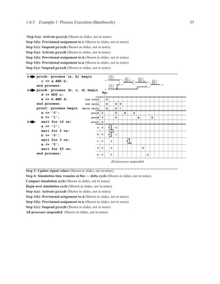
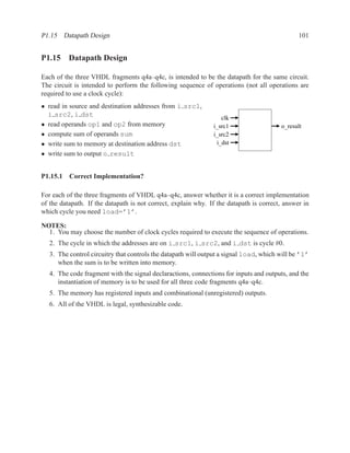
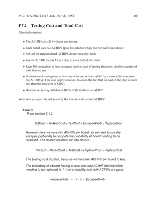
2.11.3 Data Dependencies
Definition of Three Types of Dependencies ..............................................
There are three types of data dependencies. The names come from pipeline terminology in com-
puter architecture.
M[i] := M[i] := := M[i]
:= := :=
:= M[i] M[i] := M[i] :=
Read after Write Write after Write Write after Read
(True dependency) (Load dependency) (Anti dependency)
Instructions in a program can be reordered, so long as the data dependencies are preserved.](https://image.slidesharecdn.com/vhdlreference-111231052552-phpapp02/85/VHDL-Reference-221-320.jpg)
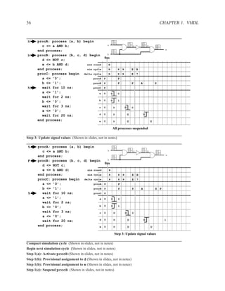
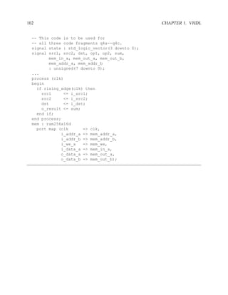
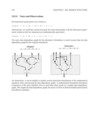
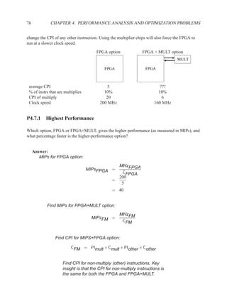
![200 CHAPTER 2. RTL DESIGN WITH VHDL
Purpose of Dependencies ............................................................. .
W0 R3 := ......
WAW ordering prevents W0
from happening after W1
W1 R3 := ...... producer
RAW ordering prevents R1
from happening before W1
R1 ... := ... R3 ... consumer
WAR ordering prevents W2
from happening before R1
W2 R3 := ......
Each of the three types of memory dependencies (RAW, WAW, and WAR) serves a specific purpose
in ensuring that producer-consumer relationships are preserved.
Ordering of Memory Operations .......................................................
M[3] M[2] M[1] M[0]
30 20 10 0
M[2] := 21 21 M[2] := 21 M[2] := 21
M[3] := 31 B := M[0] B := M[0]
A := M[2] A := M[2] A := M[2]
B := M[0] M[3] := 31 M[3] := 31
M[3] := 32 M[3] := 32 C := M[3]
M[0] := 01 M[0] := 01 M[3] := 32
C := M[3] C := M[3] M[0] := 01
Initial Program with Dependencies Valid Modification Valid (or Bad?) Modification
Answer:
Bad modification: M[3] := 32 must happen before C := M[3].](https://image.slidesharecdn.com/vhdlreference-111231052552-phpapp02/85/VHDL-Reference-222-320.jpg)
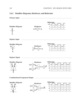
![2.11.4 Memory Arrays and Dataflow Diagrams 201
2.11.4 Memory Arrays and Dataflow Diagrams
Legend for Dataflow Diagrams .........................................................
name
name name name (rd) name(wr)
Input port Output port State signal Array read Array write
Basic Memory Operations .............................................................
mem data addr
mem addr
mem(rd) mem(wr)
mem
data
(anti-dependency) mem
data := mem[addr]; mem[addr] := data;
Memory Read Memory Write
Dataflow diagrams show the dependencies between operations. The basic memory operations are
similar, in that each arrow represents a data dependency.
There are a few aspects of the basic memory operations that are potentially surprising:
• The anti-dependency arrow producing mem on a read.
• Reads and writes are dependent upon the entire previous value of the memory array.
• The write operation appears to produce an entire memory array, rather than just updating an
individual element of an existing array.
Normally, we think of a memory array as stationary. To do a read, an address is given to the array
and the corresponding data is produced. In datalfow diagrams, it may be somewhat suprising to
see the read and write operations consuming and producing memory arrays.
Our goal is to support memory operations in dataflow diagrams. We want to model memory oper-
ations similarly to datapath operations. When we do a read, the data that is produced is dependent
upon the contents of the memory array and the address. For write operations, the apparent depen-
dency on, and production of, an entire memory array is because we do not know which address
in the array will be read from or written to. The antidependency for memory reads is related to
Write-after-Read dependencies, as discussed in Section 2.11.3. There are optimizations that can
be performed when we know the address (Section 2.11.4).](https://image.slidesharecdn.com/vhdlreference-111231052552-phpapp02/85/VHDL-Reference-223-320.jpg)
![202 CHAPTER 2. RTL DESIGN WITH VHDL
Dataflow Diagrams and Data Dependencies . . . . . . . . . . . . . . . . . . . . . . . . . . . . . . . . . . . . . . . . . . . ..
Algo: mem[wr addr] := data in; Algo: mem[wr addr] := data in;
data out := mem[rd addr]; data out := mem[rd addr];
mem data_in wr_addr mem data_in wr_addr
rd_addr
mem(wr) rd_addr
mem(wr) mem(rd)
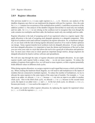
mem(rd) mem data_out
Optimization when rd addr = wr addr
mem data_out
Read after Write
Algo: mem[wr1 addr] := data1;
mem[wr2 addr] := data2;
mem data1 wr1_addr
mem(wr) data2 wr2_addr
mem(wr)
mem
Write after Write](https://image.slidesharecdn.com/vhdlreference-111231052552-phpapp02/85/VHDL-Reference-224-320.jpg)
![2.11.4 Memory Arrays and Dataflow Diagrams 203
Algo: mem[wr1 addr] := data1;
mem[wr2 addr] := data2;
mem data2 wr2_addr
mem(wr)
data1 wr1_addr
mem(wr)
mem
Scheduling option when
wr1 addr = wr2 addr
Algo: rd data := mem[rd addr]; Algo: rd data := mem[rd addr];
mem[wr addr] := wr data; mem[wr addr] := wr data;
mem rd_addr mem rd_addr wr_data wr_addr
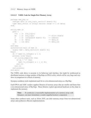
mem(rd) mem(wr)
mem(rd) wr_data wr_addr
rd_data mem
mem(wr)
Optimization when rd addr = wr addr
rd_data mem
Write after Read](https://image.slidesharecdn.com/vhdlreference-111231052552-phpapp02/85/VHDL-Reference-225-320.jpg)
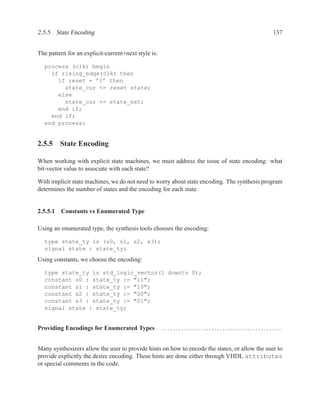
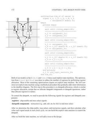
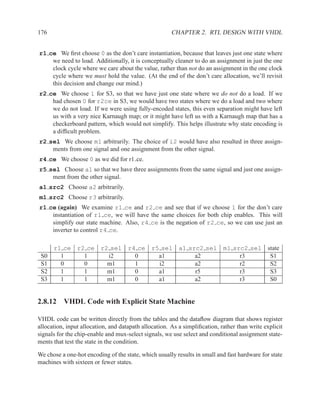
![204 CHAPTER 2. RTL DESIGN WITH VHDL
2.11.5 Example: Memory Array and Dataflow Diagram
mem data_in wr_addr
M 21 2
1 M(wr) 31 3
2 M(wr) 2 0
3 M(rd) 4 M(rd) 32 3
1 M[2] := 21 A B 5 M(wr) 01 0
2 M[3] := 31
3 A := M[2] 6 M(wr) 3
4 B := M[0]
5 M[3] := 32
7 M(rd)
6 M[0] := 01
7 C := M[3]
M C
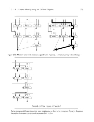
Figure 2.9: Memory array example code and initial dataflow diagram
The dependency and anti-dependency arrows in dataflow diagram in Figure2.9 are based solely
upon whether an operation is a read or a write. The arrows do not take into account the address
that is read from or written to.
In figure2.10, we have used knowledge about which addresses we are accessing to remove un-
needed dependencies. These are the real dependencies and match those shown in the code fragment
for figure2.9. In figure2.11 we have placed an ordering on the read operations and an ordering on
the write operations. The ordering is derived by obeying data dependencies and then rearranging
the operations to perform as many operations in parallel as possible.](https://image.slidesharecdn.com/vhdlreference-111231052552-phpapp02/85/VHDL-Reference-226-320.jpg)
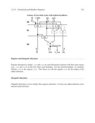
![208 CHAPTER 2. RTL DESIGN WITH VHDL
sum5 = x2 + x3 + x4 + x5
sum6 = x3 + x4 + x5 + x6
sum7 = x4 + x5 + x6 + x7
We see that part of the calculations that are done for index i are the same as those for i + 1:
sum5 = x2 + (x3 + x4 + x5 )
sum6 = (x3 + x4 + x5 ) + x6
= sum5 − x2 + x6
We check a few more samples and conclude that we can generalize the above for index i as:
sumi = sumi−1 − xi−4 + xi
avgi = sumi /4
The equation for sumi is dependent on xi and xi−4 , therefore we need the current input value and we
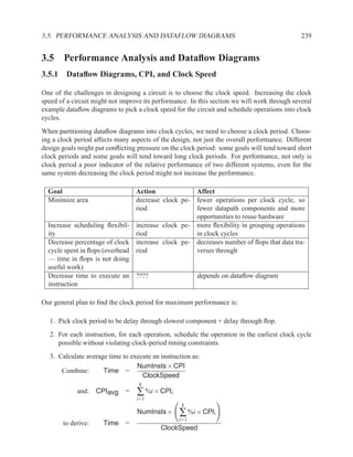
need to store the four most recent input data. These four most recent data form a sliding window:
each time we receive valid data, we remove the oldest data value (xi−4 ) and insert the new data (xi ).
Summary of system behaviour deduced from exploring requirements and algorithm:
1. Define a signal new for the value of i data each time that i valid is ’1’.
2. Define a memory array M to store a sliding window of the four most recent values of i data.
3. Define a signal old for the oldest data value from the sliding window.
4. Update sumi with sumi−1 – oldi + newi
Sliding Window .......................................................................
There are two principal ways to implement a sliding window:
shift-register Each time new data is loaded, all of the registers are loaded with the data in the
register to their right or left and the leftmost or rightmost register is loaded with new data:
R[0] = new and R[i] = R[i − 1].
circular buffer Once a data value is loaded into the buffer, the data remains in the same location
until it is overwritten. When new a value is loaded, the new value overwrites the oldest value
in the buffer. None of the other elements in the buffer change. A state machine keeps track
of the position (address) of the oldest piece of data. The state machine increments to point
to the next register, which now holds the oldest piece of data.](https://image.slidesharecdn.com/vhdlreference-111231052552-phpapp02/85/VHDL-Reference-230-320.jpg)
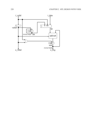
![2.13.2 Algorithm 209
old M[0..3] new
ε
old M[3] M[2] M[1] M[0] new α β γ δ
α α β γ δ ε α
ζ
ε β γ δ
β β γ δ ε ζ β
η
γ γ δ ε ζ η ε ζ γ δ
γ
ι
δ δ ε ζ η ι ε ζ η δ
δ
ε ε ζ η ι κ κ
ε ζ η ι
ζ ζ η ι κ λ ε
λ
Shift register κ ζ η ι
ζ
Circular Buffer
The circular buffer design is usually preferable, because only one element changes value per clock
cycle. This allows the buffer to implemented with a memory array rather than a set of regis-
ters. Also, by having only element change value, power consumption is reduced (fewer capacitors
charging and discharging).
We have only four items to store, so we will use registers, rather than a memory array. For less than
sixteen items, registers are generally cheaper. For sixteen items, the choice between registers and
a memory array is highly dependent on the design goals (e.g. speed vs area) and implementation
technology.
Now that we have designed the storage module, we see that rather than a write-enable and address
signal, the actual signals we need are four chip-enable signals. This suggests that we should use a
one-hot encoding for the index of the oldest element in the circular buffer.
Because we have a one-hot encoding for the index, we do not use normal multiplexers to select
which register to read from. Normal multiplexers take a binary-encoded select signal. Instead, we
will use a 4:1 decoded mux, which is just four AND gates followed by a 4-input OR gate. Because
the data is 8-bits wide, each of the AND gates and the OR gate are 8-bits wide.](https://image.slidesharecdn.com/vhdlreference-111231052552-phpapp02/85/VHDL-Reference-231-320.jpg)
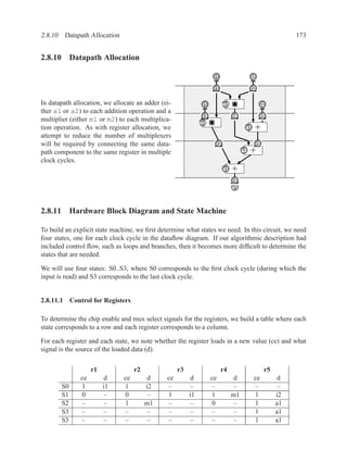
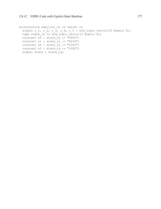
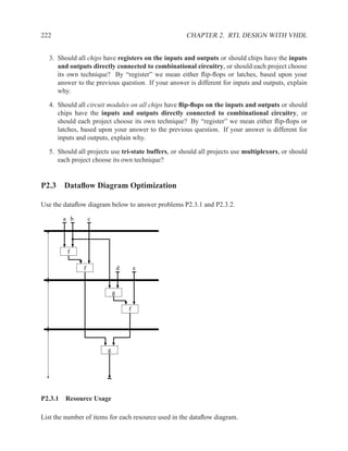
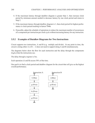
![210 CHAPTER 2. RTL DESIGN WITH VHDL
8
d M[0] 8
D Q
we ce[0]
idx[0] CE
addr
M[1] 8
D Q
ce[1]
idx[1] CE
8
q
M[2] 8
D Q
ce[2]
idx[2] CE
M[3] 8
D Q
ce[3]
idx[3] CE
Register array with chip-enables and decoded multiplexer
2.13.3 Pseudocode and Dataflow Diagrams
There are three different notations that we use to describe the behaviour of hardware systems
abstractly: mathematical equations (for datapath centric designs), state machines (for control-
dominated designs), and pseudocode (for algorithms or designs with memory). Our pseudocode is
similar to three-address assembly code: each line of code has a target variable, an operation, and
one or two operand variables (e.g., C = A + B). The name “three address” comes from the fact
that there are three addresses, or variables, in each line.
We use the three-address style of pseudocode, because each line of pseudocode then corresponds
to a single datapath operation in the dataflow diagram. This gives us greater flexibility to optimize
the pseudocode by rescheduling operations.
From the three-address pseudocode, we will construct dataflow diagrams.
As an aside, in constrast to three-address languages, some assembly languages for extremely small
processors are limited to two addresses. The target must be the same as one of the operands (e.g.,
A = A + B).](https://image.slidesharecdn.com/vhdlreference-111231052552-phpapp02/85/VHDL-Reference-232-320.jpg)
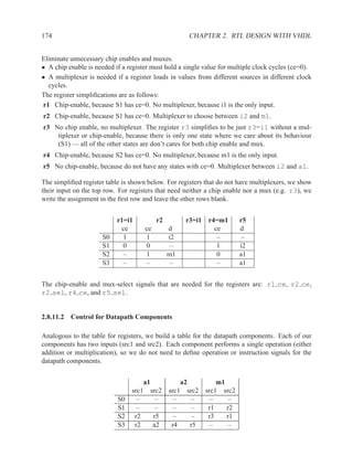
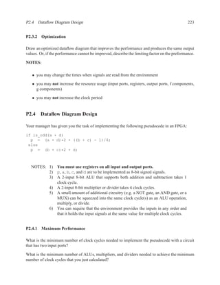
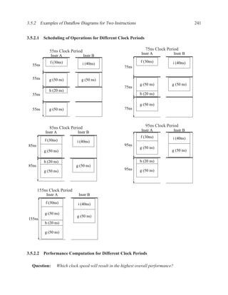
![2.13.3 Pseudocode and Dataflow Diagrams 211
First Pseudocode ......................................................................
For the first pseudocode, we do not restrict ourselves to three-addresses. In the second version of
the code, we decompose the first line into two separate lines that obey the three-address restriction.
Pseudo pseudocode
Real 3-address pseudocode
new = i_data
new = i_data
old = M[idx]
old = M[idx]
sum = sum - old + new
tmp = sum - old
M[idx] = new
sum = tmp + new
idx = idx rol 1
M[idx] = new
o_avg = sum/4
idx = idx rol 1
o_avg = sum/4
Data-Dependency Graph ............................................................. .
To begin to understand what the hardware might be, we draw a data-dependency graph for the
pseudocode.
sum M idx i_data
new
Rd
old
Wr
1
tmp
(wired shift)
sum o_avg M idx
Optimizing the Data-Dependency Graph .............................................. .
In our design work so far, we have ignored bubbles and time. As we evolve from the pseudocode
to a datadependency graph and then to a dataflow graph, we will include the effect of the bubbles
in our analysis.](https://image.slidesharecdn.com/vhdlreference-111231052552-phpapp02/85/VHDL-Reference-233-320.jpg)
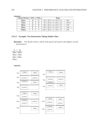
![2.13.3 Pseudocode and Dataflow Diagrams 213
Data-dependency graph after removing new
Remove intermediate signal old
new = i_data sum M idx i_data
tmp = sum - M[idx]
sum = tmp + new
M[idx] = new
idx = idx rol 1
Rd
o_avg = sum/4
Optimize code byreading new from memory old
tmp = sum - M[idx] Wr
M[idx] = i_data
new = M[idx]
sum = tmp + new Rd
idx = idx rol 1 1
o_avg = sum/4
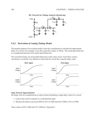
tmp new
Remove intermediate signal new
tmp = sum - M[idx] (wired shift)
M[idx] = i_data
sum = tmp + M[idx]
idx = idx rol 1 sum o_avg M idx
o_avg = sum/4
Dataflow Diagram .....................................................................
To construct a dataflow diagram, we divide the data-dependency graph into clock cycles. Because
we are using registers rather than a memory array, we can schedule the first read and first write
operations in the same clock cycle, even though they use the same address. In contrast, with
memory arrays it generally is risky to rely on the value of the output data in the clock cycle in
which we are doing a write (Section 2.11.1).
We need a second clock cycle for the second read from memory.
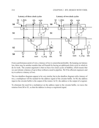
We now explore two options: with and without a third clock cycle; both are shown below. The
difference between the two options is whether the signals idx and sum refers to the output of
registers or the combinational datapath units (sum being the output of the adder/subtracter and
idx being the output of a rotation). With a latency of three clock cycles, idx is a registered
signal. With a latency of two clock cycles, idx and sum are combinational.
It is a bit misleading to describe the rotate-left unit for idx as combinational, because it is simply
a wire connecting one flip-flop to another. However, conceptually and for correct behaviour, it
is helpful to think of the rotation unit as a block of combinational circuitry. This allows us to
distinguish between the output of the idx register and the input to the register (which is the output
of the rotation unit). Without this distinction, we might read the wrong value of idx and be
out-of-sync by one clock cycle.](https://image.slidesharecdn.com/vhdlreference-111231052552-phpapp02/85/VHDL-Reference-235-320.jpg)


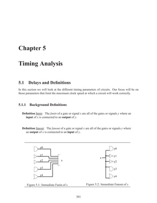
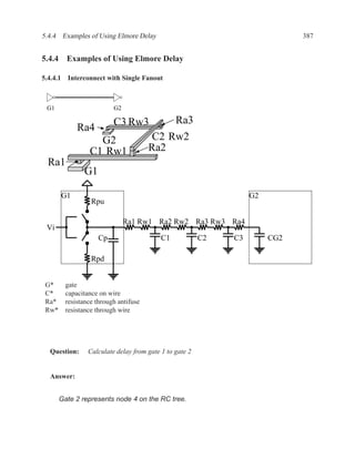
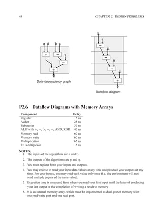
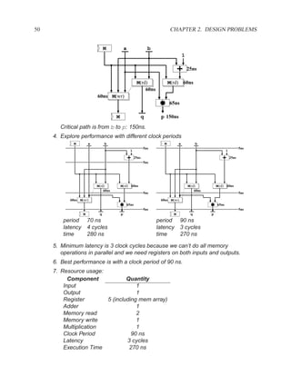
![P2.7 2-bit adder 225
8. Assume all memory address and other arithmetic calculations are within the range of repre-
sentable numbers (i.e. no overflows occur).
9. If you need a circuit not on the list above, assume that its delay is 30 ns.
10. You may sacrifice area efficiency to achieve high performance, but marks will be deducted
for extra hardware that does not contribute to performance.
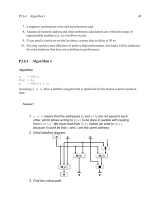
P2.6.1 Algorithm 1
Algorithm
q = M[b];
M[a] = b;
p = M[b+1] * a;
Assuming a ≤ b, draw a dataflow diagram that is optimized for the fastest overall execution
time.
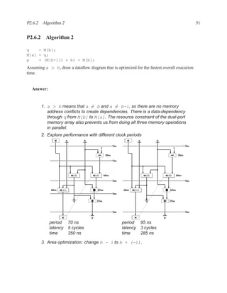
P2.6.2 Algorithm 2
q = M[b];
M[a] = q;
p = (M[b-1]) * b) + M[b];
Assuming a > b, draw a dataflow diagram that is optimized for the fastest overall execution
time.
P2.7 2-bit adder
This question compares an FPGA and generic-gates implementation of 2-bit full adder.
P2.7.1 Generic Gates
Show the implementation of a 2 bit adder using NAND, NOR, and NOT gates.](https://image.slidesharecdn.com/vhdlreference-111231052552-phpapp02/85/VHDL-Reference-247-320.jpg)
![226 CHAPTER 2. RTL DESIGN WITH VHDL
P2.7.2 FPGA
Show the implementation of a 2 bit adder using generic FPGA cells; show the equations for the
lookup tables.
c_in
sum[0]
a[0]
b[0]
comb R
D Q
CE
S
carry_1
sum[1]
a[1]
b[1]
comb R
D Q
CE
S
c_out
P2.8 Sketches of Problems
1. calculate resource usage for a dataflow diagram (input ports, output ports, registers, datapath
components)
2. calculate performance data for a dataflow diagram (clock period and number of cycles to
execute (CPI))
3. given a dataflow diagram, calculate the clock period that will result in the optimum perfor-
mance
4. given an algorithm, design a dataflow diagram
5. given a dataflow diagram, design the datapath and finite state machine
6. optimize a dataflow diagram to improve performance or reduce resource usage
7. given fsm diagram, pick VHDL code that “best” implements diagram — correct behaviour,
simple, fast hardware — or critique hardware](https://image.slidesharecdn.com/vhdlreference-111231052552-phpapp02/85/VHDL-Reference-248-320.jpg)


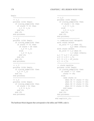
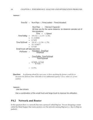
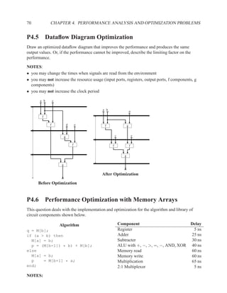
![P3.6 Performance Optimization with Memory Arrays 259
a b c
a b
d
f
f d e f g
g c e
f f f
g
g
After Optimization
Before Optimization
P3.6 Performance Optimization with Memory Arrays
This question deals with the implementation and optimization for the algorithm and library of
circuit components shown below.
Algorithm Component Delay
q = M[b]; Register 5 ns
if (a > b) then Adder 25 ns
M[a] = b; Subtracter 30 ns
p = (M[b-1]) * b) + M[b]; ALU with +, −, >, =, −, AND, XOR 40 ns
else Memory read 60 ns
M[a] = b; Memory write 60 ns
p = M[b+1] * a; Multiplication 65 ns
end; 2:1 Multiplexor 5 ns
NOTES:
1. 25% of the time, a > b
2. The inputs of the algorithm are a and b.
3. The outputs of the algorithm are p and q.
4. You must register both your inputs and outputs.
5. You may choose to read your input data values at any time and produce your outputs at any
time. For your inputs, you may read each value only once (i.e. the environment will not send
multiple copies of the same value).
6. Execution time is measured from when you read your first input until the latter of producing
your last output or the completion of writing a result to memory](https://image.slidesharecdn.com/vhdlreference-111231052552-phpapp02/85/VHDL-Reference-281-320.jpg)


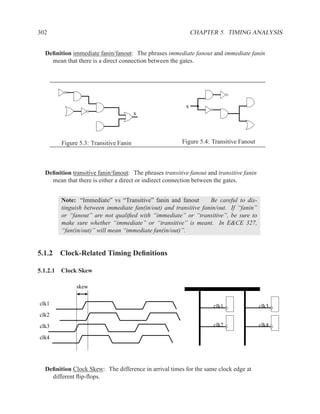
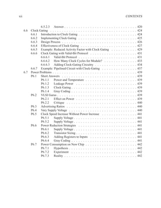
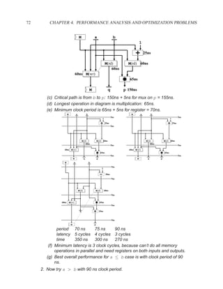
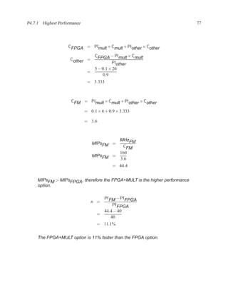
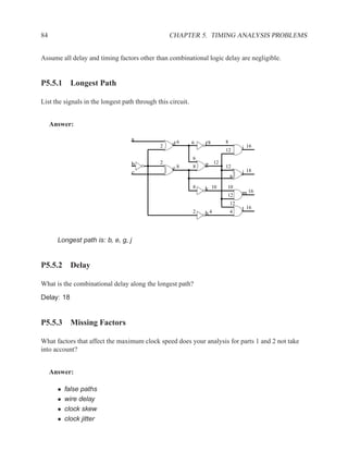
![350 CHAPTER 5. TIMING ANALYSIS
d f g
a j
1 ‘1’ l
b 0 ‘0’ h ‘1’
‘1’ k
m
i
e ‘0’
c
Contradictory values.
side input non-controlling value constraint
g[b] 1 b
i[e] 0 c
k[h] 1 b
Found contradiction between g[b] needing b and k[h] needing b, therefore the
candidate path is a false path.
Analyze cause of contradiction:
d f g
a j
l
h
b
k
m
i
e 2
c
These side inputs will always have
opposite values. Both side inputs
feed the same type of gate (AND),
so it always be the case that one of the
side inputs will be a controlling value (0).
False-Path Example 2 ................................................................ .
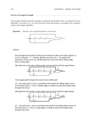
Question: Determine if the longest path through the circuit below is a critical path.
If the longest path is a critical path, find a pair of input vectors that will exercise the
path.
d
a f
b
h
g
e
c](https://image.slidesharecdn.com/vhdlreference-111231052552-phpapp02/85/VHDL-Reference-372-320.jpg)
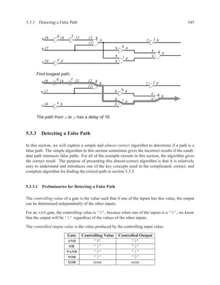
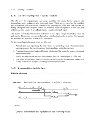
![5.3.3 Detecting a False Path 351
Answer:
d
a f
b
‘1’
‘0’ h
‘1’ g
e
c
side input non-controlling value constraint
e[a] 1 a
g[b] 0 b
h[f] 1 a+b
Complete constraint is conjunction of constraints: ab(a + b), which reduces to
false. Therefore, the candidate path is a false path.
False-Path Example 3 ................................................................ .
This example illustrates a candidate path that is a true path.
Question: Determine if the longest path through the circuit below is a critical path. If
the longest path is a critical path, find a pair of input vectors that will exercise the
path.
d
a f
b
h
g
e
c
Answer:
Find longest path; label side inputs with non-controlling values:
d
a f
b
‘1’
‘0’ h
‘0’ g
e
c](https://image.slidesharecdn.com/vhdlreference-111231052552-phpapp02/85/VHDL-Reference-373-320.jpg)
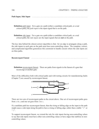
![352 CHAPTER 5. TIMING ANALYSIS
Table of side inputs, non-controlling values, and constraints on primary inputs:
side input non-controlling value constraint
e[a] 0 a
g[b] 0 b
h[b] 1 a+b
The complete constraint is ab(a + b), which reduces to ab. Thus, for an edge
to propagate along the path, a must be ’0’ and b must be ’0’.
The primary input to the path (c) does not appear in the constraint, thus both
rising and falling edges will propagate along the path. If the primary input to
the path appears with a positive polarity (e.g. c) in the constraint, then only a
rising edge will propagate. Conversely, if the primary input appears negated
(e.g., c), then only a falling edge will propagate.
Critical path c, e, g, h
Delay 14
Input vector a=0, b=0, c=rising edge
Illustration of rising edge propagating along path:
d‘1’
a‘0’ ‘1’ f‘1’
b‘0’ ‘0’
‘1’
‘0’ h
‘0’ g
e
c
Illustration of falling edge propagating along path:
d‘1’
a‘0’ ‘1’ f‘1’
b‘0’ ‘0’
‘1’
‘0’ h
‘0’ g
e
c
False-Path Example 4 ................................................................ .
This example illustrates reconvergent fanout.](https://image.slidesharecdn.com/vhdlreference-111231052552-phpapp02/85/VHDL-Reference-374-320.jpg)
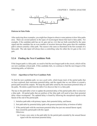
![5.3.3 Detecting a False Path 353
Question: Determine if the longest path through the circuit below is a critical path. If
the longest path is a critical path, find a pair of input vectors that will exercise the
path.
c d
a g
e f
b
Answer:
c d
a ‘1’ g
e f
b ‘1’
side input non-controlling value constraint
e[b] 1 b
g[d] 1 a
The complete constraint is ab.
The constraint includes the input to the path (a), which indicates that not all
edges will propagate along the path. The polarity of the path input indicates
the final value of the edge. In this case, the constraint of a means that we
need a rising edge.
Critical path a, c, e, f, g
Delay 12
Input vector a=rising edge, b=1
Illustration of rising edge propagating along path:
c d
a g
e f
b‘1’ ‘1’
If we try to propagate a falling edge along the path, the falling edge on the
side input d forces the output g to fall before the arrival of the falling edge on
the path input f. Thus, the edge does not propagate along the candidate
path.](https://image.slidesharecdn.com/vhdlreference-111231052552-phpapp02/85/VHDL-Reference-375-320.jpg)
![356 CHAPTER 5. TIMING ANALYSIS
Path table and constraint table after detecting that the longest path is a false
path:
potential unused
delay fanout path
10 e c
12 h, g b
16 j, i a, d, f, g
false a, d, f, g, i, k
side input non-controlling value constraint
g[b] 1 b
i[e] 0 c
k[h] 1 b
The longest path is a false path. Recompute potential delay of all paths in
path table that are prefixes of the false path.
The one path that is a prefix of the false path is: a,d,f,g . The remaining
unused fanout of this path is j, which has a potential delay on its input of 2.
The previous potential delay of g was 8, thus the potential delay of the prefix
reduces by 8 − 2 = 6, giving the path a potential delay of 16 − 6 = 10.
Path table after updating with new potential delays:
potential unused
delay fanout path
false a, d, f, g, i, k
10 e c
10 i a, d, f, g
12 h, g b
Extend b through g, because g has greater potential delay than the other
fanout signal (h).
potential unused
delay fanout path
false a, d, f, g, i, k
10 e c
10 i a, d, f, g
12 h, g b
12 i, j b, g
side input non-controlling value constraint
g[a] 1 a
From g, we will follow i, because it has greater potential delay than j.](https://image.slidesharecdn.com/vhdlreference-111231052552-phpapp02/85/VHDL-Reference-378-320.jpg)
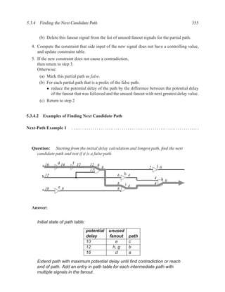
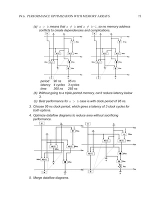
![5.3.4 Finding the Next Candidate Path 357
potential unused
delay fanout path
false a, d, f, g, i, k
10 e c
10 i a, d, f, g
12 h, g b
12 i, j b, g
12 b, g, i, k
side input non-controlling value constraint
g[a] 1 a
i[e] 0 c
k[h] 1 b
We have reached an output without encountering a contradiction in our
constraints. The complete constraint is abc.
Critical path b, g, i, k
Delay 12
Input vector a=1, b=falling edge, c=1
Illustrate the propagation of a falling edge:
d f g
a‘1’ ‘1’
2 j
h
b
k
i
e
c‘1’ ‘0’
At k, the rising edge on the side input (h) arrives before the falling edge on
the path input (i). For a brief moment in time, both the side input and path
input are ’1’, which produces a glitch on k.
Next-Path Example 2 ..................................................................
Question: Find the critical path in the circut below
a l m
m
b j
i
c g h
f
d
k
k
e](https://image.slidesharecdn.com/vhdlreference-111231052552-phpapp02/85/VHDL-Reference-379-320.jpg)
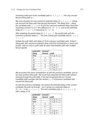
![358 CHAPTER 5. TIMING ANALYSIS
Answer:
Find the longest path:
a 10 6
l 2 m 0
m
b 14 10 j
6
14 6
i 10
c 20 20
g 16 h 14
10
f
d 22 20
4
k 0 0
4 4 k
e
Initial state of path table:
potential unused
delay fanout path
4 k e
10 j, l a
14 i b
20 g c
22 f d
Extend path with maximum potential delay until find contradiction or reach
end of path. Add an entry in path table for each intermediate path with
multiple fanout signals.
potential unused
delay fanout path
4 k e
10 j, l a
14 i b
20 g c
22 j, k d, f, g, h, i
false d, f, g, h, i, j, l
side input non-controlling value constraint
g[c] 1 c
i[b] 0 b
j[a] 0 a
l[a] 1 a
Contradiction between j[a] and l[a], therefore the path d,f,g,h,i,j,l is
a false path. And, any path that extends this path is also false.
To find next candidate, begin by recomputing delays along the candidate
path. The second gate in the contradiction is l. The last intermediate path
before l with unused fanout is i. Cut the candidate path at this signal. The](https://image.slidesharecdn.com/vhdlreference-111231052552-phpapp02/85/VHDL-Reference-380-320.jpg)
![360 CHAPTER 5. TIMING ANALYSIS
We extend the path through k and compute the constraint table.
side input non-controlling value constraint
g[c] 1 c
i[b] 0 b
k[e] 0 e
The complete constraint is bce. There is no constraint on a and d may be
either a rising edge or a falling edge.
Critical path d, f, g, h, i, k
Delay 16
Input vector a=0, b=0, c=1, d=rising edge, e=0
Next Path Example 3 ................................................................. .
Question: Find the critical path in the circuit below.
j
a l
m
k m
e
b
f g h i
c n
p
p
o
d
Answer:
j
a 12 10 8 8
l
4 4 m 0
12 k 8
m
8 4
14 e 12
b
f g h i 8
c 16 8 n 4
8 4 p 0
4 p
8 6 o4
d
Initial state of path table:](https://image.slidesharecdn.com/vhdlreference-111231052552-phpapp02/85/VHDL-Reference-382-320.jpg)
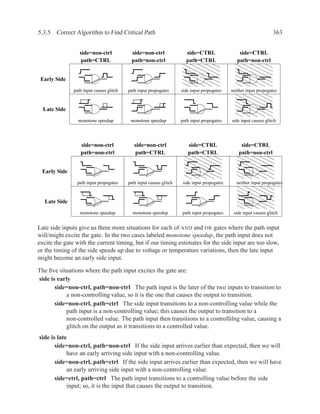
![5.3.4 Finding the Next Candidate Path 361
potential unused
delay fanout path
8 n, o d
12 j, k a
14 e b
16 f c
Extend c through f:
potential unused
delay fanout path
8 n, o d
12 j, k a
14 e b
16 m, n c,f,g,h,i
false c,f,g,h,i,n,p
side input non-controlling value constraint
n[d] 1 d
p[o] 1 d
The first candidate is a false path. Recompute potential delay of c, f, g, h, i,
which reduces it from 16 to 12.
potential unused
delay fanout path
false c,f,g,h,i,n,p
8 n, o d
12 j, k a
12 m c,f,g,h,i
14 e b
Extend b through e:
potential unused
delay fanout path
false c,f,g,h,i,n,p
8 n, o d
12 j, k a
12 m c,f,g,h,i
false b,e,k,l
side input non-controlling value constraint
k[a] 1 a
l[j] 1 a](https://image.slidesharecdn.com/vhdlreference-111231052552-phpapp02/85/VHDL-Reference-383-320.jpg)
![362 CHAPTER 5. TIMING ANALYSIS
The second candidate is a false path. There is no unused fanout signal from
l for the path b, e, k, l, so this partial path is a false path and there is no new
delay information to compute.
There are two paths with a potential delay of 12. Choose c, f, g, h, i ,
because the end of the path is closer to an output, so there will be less work
to do in analyzing the path.
potential unused
delay fanout path
false c,f,g,h,i,n,p
false b,e,k,l
8 n, o d
12 j, k a
12 c,f,g,h,i,m
side input non-controlling value constraint
m[l] 0 ¬(a ∗ (ab)) = true
Critical path c,f,g,h,i,m
Delay 12
Input vector a=0, b=1, c=rising edge, d=0
5.3.5 Correct Algorithm to Find Critical Path
In this section, we remove the assumption that values on side inputs always arrive earlier than the
value on the path input. We now deal with late arriving side inputs, or simply “late side inputs”.
The presentation of late side inputs is as follows:
Section 5.3.5.1 rules for how late side inputs can allow path inputs to exercise gates
Section 5.3.5.2 idea of monotone speedup, which underlies some of the rules
Section 5.3.5.3 one of the potentially confusing situations in detail.
Section 5.3.5.4 complete, correct, and complex algorithm.
Section 5.3.5.5 examples
5.3.5.1 Rules for Late Side Inputs
For each gate, there are eight sitations: the side input is controlling or non-controlling, the path
input is controlling or non-controlling, and the side input arrives early or arrives late.](https://image.slidesharecdn.com/vhdlreference-111231052552-phpapp02/85/VHDL-Reference-384-320.jpg)
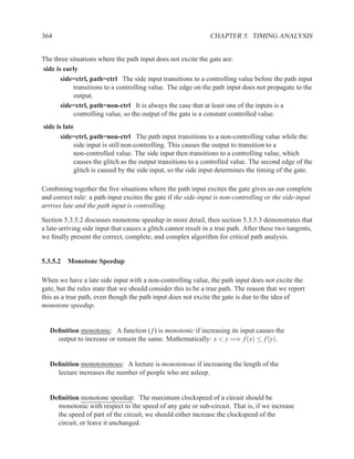
![368 CHAPTER 5. TIMING ANALYSIS
potential unused
delay fanout path
14 g, b, c a
false a,b,d,e,f,g
side input non-controlling value constraint
f[c] 1 a
g[a] 1 a
First false path, pursue next candidate.
potential unused
delay fanout path
false a,b,d,e,f,g
10 g, c a
10 a,c,f,g
side input non-controlling value constraint
f[e] 1 a
g[a] 1 a
At first, this path appears to be false, but the side input f[e] is on the prefix
of the false path a,b,d,e,f,g. Thus, f[e] is a late arriving side input.
The candidate path will be a true path if the side input arrives late and the
path input is a controlling value. The viability condition for the path a,b,d,e is
true. The constraint for the path input (c) to have a controlling value for f is a.
Together, the viability constraint of true and the controlling value constraint of
a give us a late-side constraint of a.
Updating the constraint table with the late arriving side input constraint gives
us:
side input non-controlling value constraint
f[e] 1 a + a = true
g[a] 1 a
The constraint reduces to a. A rising edge will exercise the path.
Critical path a, c, f, g
Delay 10
Input vector a=rising edge
Illustration of rising edge exercising the critical path:
0
0 0 2 4 6 10
b d e g
a f6
2
0
c](https://image.slidesharecdn.com/vhdlreference-111231052552-phpapp02/85/VHDL-Reference-390-320.jpg)
![5.3.5 Correct Algorithm to Find Critical Path 369
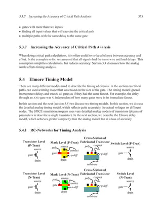
Complete Example 2 ................................................................. .
Question: Find the critical path in the circuit below.
a
d
b
i
c
Answer:
Find longest path:
8 8 f4
a
8 4 j 0
8 8 i
4 4 j
d 16 e 14 g 12 12 8
18 14 h8
b
12 12 i
c
Explore longest path:
potential unused
delay fanout path
8 f a
12 h c
18 f, g b,d,e
18 h, i b,d,e,g
false b,d,e,g,h,i,j
side input non-controlling value constraint
h[c] 0 c
i[g] 0 b
j[f] 0 ab
Contradiction.
0 f0
a
0 0 j
0 i
j
d e 0 1 g 0
b h
i
c
First false path, find next candidate.](https://image.slidesharecdn.com/vhdlreference-111231052552-phpapp02/85/VHDL-Reference-391-320.jpg)
![370 CHAPTER 5. TIMING ANALYSIS
Changes in potential delays:
Signal / path old new
g on b, d, e, g 12 8
b, d, e, g 18 14
g[e] on b, d, e 14 10
e on b, d, e 14 10
b, d, e 18 14
potential unused
delay fanout path
false b,d,e,g,h,i,j
8 f a
12 h c
14 f, g b,d,e
14 b,d,e,g,i,j
8 8 f4
a
8 4 j 0
8 8 i
4 4 j
d 12 e 10 g 8 12 8
14 10 h8
b
12 12 i
c
side input non-controlling value constraint
h[c] 0 c
i[h] 0 cb
j[f] 0 ab
Initially, found contradiction, but b, d, e, g, h is a prefix of a false path, and
i[h] is a side input to the candidate path. We have a late side input.
Note that at the time that we passed through i, we could not yet determine
that we would need to use i[h] as a late side input. The lesson is that when
a contradiction is discovered, we must look back along the entire candidate
path covered so far to see if we have any late side inputs.
Our late-arriving constraint for i[h] is:
• late side path ( b, d, e, g, h ) is viable: c.
• path input (i[g]) has a controlling value of ’1’: b.
Combining these constraints together gives us bc.
Adding the constraint of the late side input to to the condition table gives us:
side input non-controlling value constraint
h[c] 0 c
i[h] 0 bc + bc = c
j[f] 0 ab](https://image.slidesharecdn.com/vhdlreference-111231052552-phpapp02/85/VHDL-Reference-392-320.jpg)
![5.3.5 Correct Algorithm to Find Critical Path 371
The constraints reduce to abc.
Critical path b, d, e, g, i, j
Delay 14
Input vector a=0, b=falling edge, c=0
Illustration of falling edge exercising the critical path:
a
0 f 8 8
4 14
6 i j
10 10 j
0 d 2 e 4 4 g 6
h 10
b
0 i
c
Complete Example 3 . . . . . . . . . . . . . . . . . . . . . . . . . . . . . . . . . . . . . . . . . . . . . . . . . . . . . . . . . . . . . . . . . .
This example illustrates the benefits of the principle of monotone speedup when analyzing critical
paths.
b d f
a e
c
Critical-path analysis says that the critical path is a, c, e, f , with a late side input of e[d] and a
total delay of 10. The required excitation is a rising edge on a. However, with the given delays,
this excitation does not produce an edge on the output.
0
0 0 2 4
b d f
a e
0 2
c
For a more complete analysis of the behaviour, we also try a falling edge. The falling edge path
exercises the path a, f with a delay of 4.
0
0 0 2 4 4
b d 6 f
a e
0 2
c
Monotone speedup says that if we reduce the delay of any gate, we must not increase the delay of
the overall circuit. We reduce the delays of b and d from 2 to 0.5 and produce an edge at time 10
via the path a, c, e, f .](https://image.slidesharecdn.com/vhdlreference-111231052552-phpapp02/85/VHDL-Reference-393-320.jpg)
![372 CHAPTER 5. TIMING ANALYSIS
0
0 0 0.5 1 10
b d f
a e 6
0 2
c
The critical path analysis said that the critical path was a, c, e, f with a delay of 10. With the
original circuit, the slowest path appeared to have a delay of 4. But, by reducing the delays of two
gates, we were able to produce an edge with a delay of 10. Thus, the critical path algorithm did
indeed satisfy the principle of monotone speedup.
Complete Example 4 . . . . . . . . . . . . . . . . . . . . . . . . . . . . . . . . . . . . . . . . . . . . . . . . . . . . . . . . . . . . . . . . . .
This example illustrates that we sometimes need to allow edges on the inputs to late side paths.
Question: Find the critical path in the circuit below.
c d
a e k
i j
b
f g h
Answer:
The purpose of this example is to illustrate a situation where we need the
primary input of a late-side path to toggle. To focus on the behaviour of the
circuit, we show pictures of different situations and do not include the path
and constraint tables.
Longest path in the circuit, showing a contradiction between e[b] and j[h].
c d
a e k
i j
1 0
b 0
1 f 0 g 1 h
Second longest path b, f, g, h, i, j, k , using only early side inputs, showing a
contradiction between k[e] and i[e].
c d 1
a e 1 0 0
k
i j
b
f g h](https://image.slidesharecdn.com/vhdlreference-111231052552-phpapp02/85/VHDL-Reference-394-320.jpg)
![5.3.5 Correct Algorithm to Find Critical Path 373
Second longest path using late side input i[e], which has a controlling value
of 1 (rising edge) on i[h]. However, we neglect to put a rising edge on a.
The late-side path is not exercised and our candidate path is also not
exercised.
c 0 d 1
a1 0
e
1 1 i j
1 k 0
6 1 0
b
0 f 2 g 4 h 6
We now put a rising edge on a, which causes our late side input (i[e]) to be
a non-controlling value when our path input (i[h]) arrives.
0 c 2 d 4 48
a 0 e4 8 k 16
14
0 i 810 j
b 6
10 12
0 f 2 g 4 h 6
In looking at the behaviour of i, we might be concerned about the precise
timing of of the glitch on e and the rising ege on h. The figure below shows
normal, slow, and fast timing of e. With slow timing, the first edge of glitch on
e arrives after the rising edge on h. The timing of the second edge of the
glitch remains unchanged. The value of i remains constant, which could lead
us to believe (incorrectly!) that our critical path analysis needs to take into
account the first edge of the glitch. However, this is in fact an illustration of
monotone speedup. The fast timing scenario move the glitch earlier, such that
the edge on h does in fact determine the timing of the circuit, in that h
produces the last edge on i. In summary, with the glitch on e and the rising
edge on h, either h causes the last edge on i or there is no edge on i.
4 8
8 10
Normal timing e
6 i
h
4 8
8 10
Slow timing on e e
6 i
h
4 8
8 10
Fast timing on e e
6 i
h
Complete Example 5 . . . . . . . . . . . . . . . . . . . . . . . . . . . . . . . . . . . . . . . . . . . . . . . . . . . . . . . . . . . . . . . . . .
This example demonsrates that a late side path must be viable to be helpful in making a true path.
Question: Find the critical path in the circuit below.](https://image.slidesharecdn.com/vhdlreference-111231052552-phpapp02/85/VHDL-Reference-395-320.jpg)
![374 CHAPTER 5. TIMING ANALYSIS
a e
g
b i
k
c
h j
f
d
Answer:
Find that the two longest paths are false paths, because of contradiction
between g[d] and i[c].
a e
g
b 0 i
1 k
c
h j
f
d
Try third longest path d, f, h, j, k using early side inputs. Find contradiction
between k[i] and j[c].
a e
g
b i 0 1
0 1 k
c 0
0 h j
f
d
Try using late side paths a, e, g, i, k or b, e, g, i, k . Find that neither path is
viable by itself, because of contradiction between g[d] and i[c]. Also,
neither path is viable in conjunction with the candidate path, because of
contradiction between i[c] on late side path and j[c] on candidate path.
Either one of these contradictions by itself is sufficient to prevent the late side
path from helping to make the candidate path a true path.
a e
g
b i
0 1 k
c 0
0 h j
f
d
5.3.6 Further Extensions to Critical Path Analysis
McGeer and Brayton’s paper includes two extensions to the critical path algorithm presented here
that we will not cover.](https://image.slidesharecdn.com/vhdlreference-111231052552-phpapp02/85/VHDL-Reference-396-320.jpg)


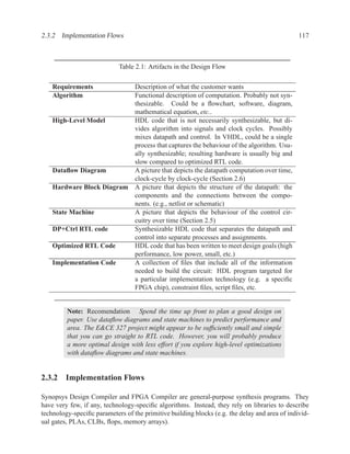
This document contains course notes for E&CE 327: Digital Systems Engineering. It provides an introduction to VHDL, including levels of abstraction, origins and history, syntax overview, processes, and simulation techniques like register-transfer level simulation. It also discusses hardware building blocks that can be modeled in VHDL and differences between synthesizable and non-synthesizable code. The document aims to explain key concepts for designing and simulating digital circuits using the VHDL hardware description language.


![[Actuary] actuarial mathematics and life table statistics](https://cdn.slidesharecdn.com/ss_thumbnails/actuaryactuarialmathematicsandlife-tablestatistics-120627131254-phpapp01-thumbnail.jpg?width=640&height=640&fit=bounds)