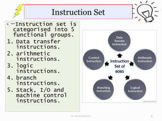
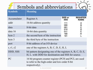
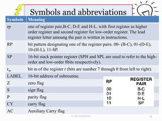
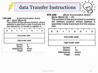
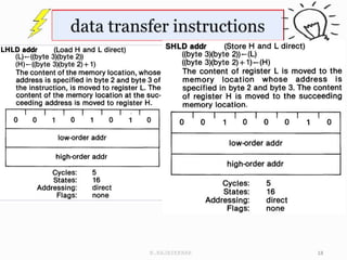
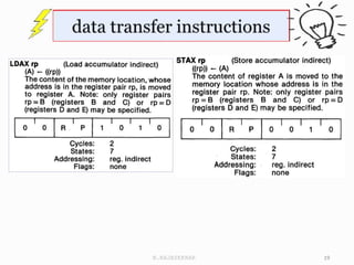
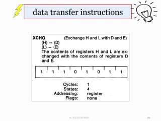
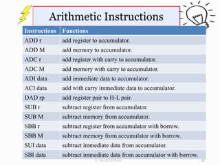
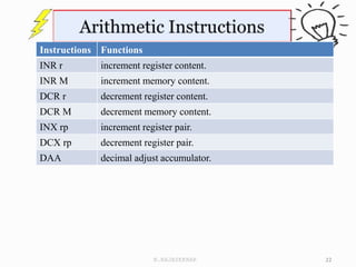
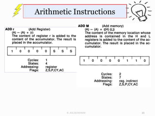
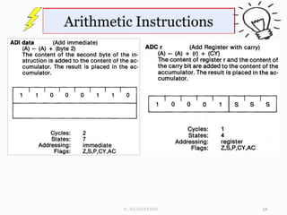
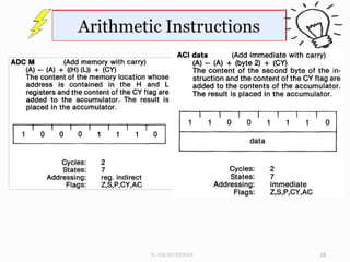
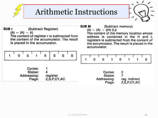
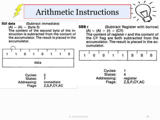
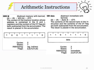
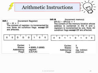
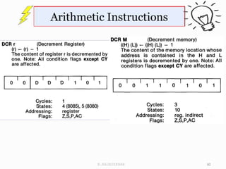
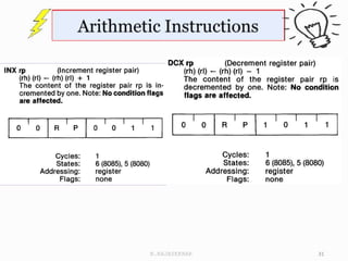
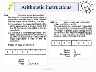
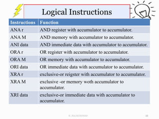
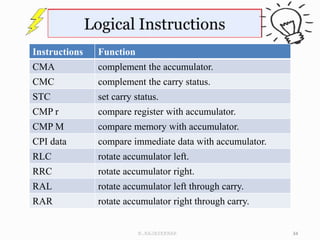
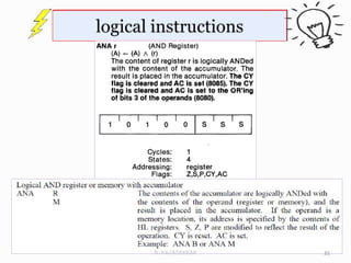
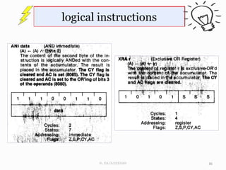
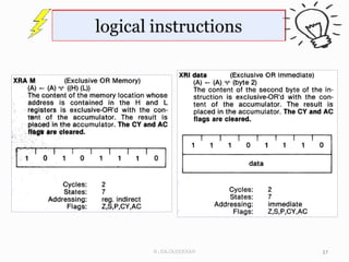
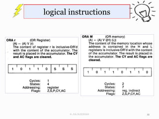
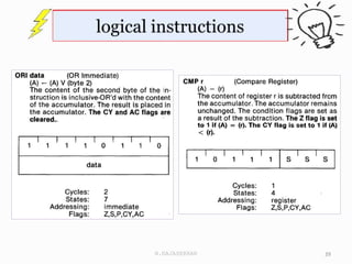
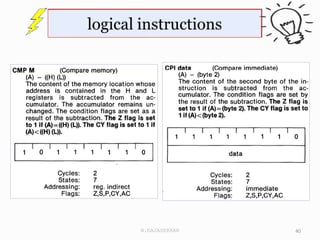
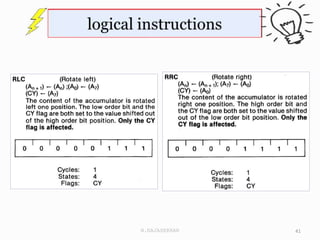
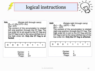
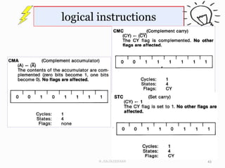
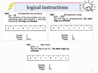
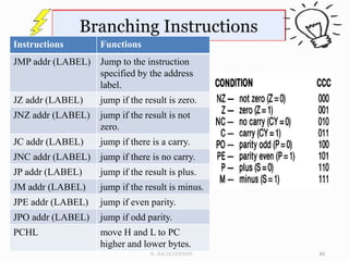
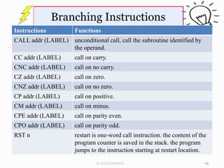
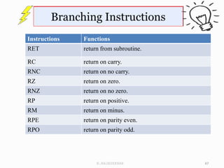
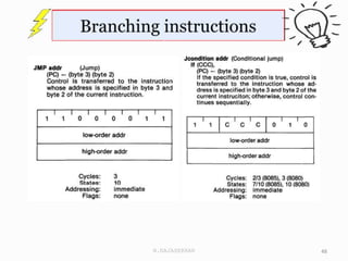
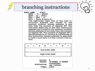
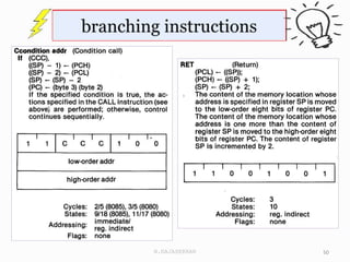
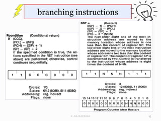
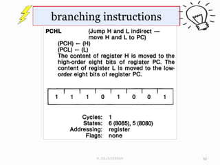
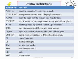
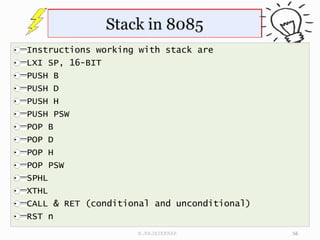
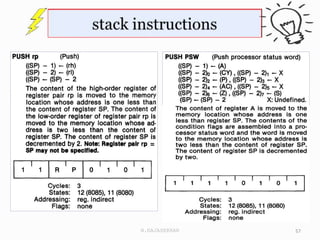
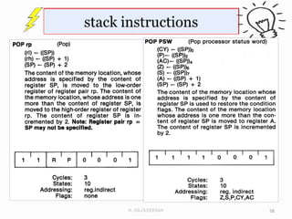
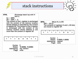
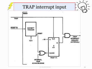
N.RAJASEKHAR
Associate Professor
Department of ECE
Lendi Institute of Engineering and Technology
1
N.RAJASEKHAR
Addressing modes.
Instruction and Data format.
Instructions set of 8085.
Interrupts of 8085.
programming of 8085 with examples.
2
N.RAJASEKHAR
once the program is placed in memory
space that is accessible to your CPU,you
may run that same sequence of
instructions as often as you wish to
solve the same problem.
The set of instructions to which the
8085A CPU will respond is permanently
fixed in the design of the chip.
when multi-byte numeric data is used,
the data,like instructions, is stored in
successive memory locations, with the
least significant byte first,followed by
increasingly significant bytes.
3
N.RAJASEKHAR
8085A has four/five different modes for
addressing data stored in memory or in
registers.
Implied addressing- instruction specifies the
data to be operated on. CMA- complement
accumulator.
Immediate Addressing- instruction contains the
data itself. this is either an 8-bit or 16 bit
quantity(in binary, least significant byte
first and most significant byte second).
Ex: MVI R,Data ( R is any register)
MVI B,4CH
Register Addressing- instruction specifies the
register or register pair in which the data is
located.
Ex: MOV Rd,Rs (Rd and Rs are 8-bit registers)
MOV D,H
4
N.RAJASEKHAR
Direct Addressing - byte 2 and 3 of the instruction
contain the exact memory address of the data item(
lower order bits of address are in byte 2, higher
order bits are in byte 3).
• LDA direct (direct is a 16bit memory address)
• LDA 2050H (A<- content of 2050H address).
Register Indirect Addressing - instruction specifies
register pair which contains the memory address where
the data is located (higher order bits are in first
register of the pair, the lower order bits in the
second).
• LXI H, 8000H (load the register pair H & L
immediate data)
• MOV M,R (M is 16bit memory pointed by H & L and R is
a register)
• MOV M,B ( copy content of B into memory pointed by
register pair H & L).
5
N.RAJASEKHAR
8085 instruction set is classified into
following three groups according to byte size.
1-byte instructions
2-byte instructions
3-byte instructions
one-byte instruction- it include the opcode
and operand in the same byte. each of the
instruction require 1 memory location.
6
N.RAJASEKHAR
two-byte instructions- the first bye specifies
the operation code and the second byte specifies
the operand (data or address).
Three byte instructions - first byte is opcde,
following two bytes specify data or address,
second byte is the lower address/data and third
byte is the higher-order address/data.
7
N.RAJASEKHAR
8
N.RAJASEKHAR
Instruction set is
categorised into 5
functional groups.
1. Data transfer
instructions.
2. arithmetic
instructions.
3. logic
instructions.
4. branch
instructions.
5. Stack, I/O and
machine control
instructions.
9
N.RAJASEKHAR
Symbols Meaning
Accumulator Register A
addr 16-bit address quantity
data 8-bit data
data 16 16-bit data quantity
byte 2 the second byte of the instruction.
byte 3 the third byte of the instruction
port 8-bit address of an I/O device
r, r1, r2 one of the registers A, B, C, D, E, H, L
DDD, SSS bit pattern designating one of the registers A, B, C, D, E,
H, L. with DDD for desitination and SSS for source.
PC 16 bit program counter register (PCH and PCL are used
to refer to the high-order and low-order 8-bit
respectively).
10
N.RAJASEKHAR
Symbols Meaning
rp one of register pair,B-C, D-E and H-L. with first register as higher
order register and second register for low-order register. The lead
register letter amoung the pair is written in instructions.
RP bit pattern designating one of the register pairs. 00- (B-C), 01-(D-E),
10-(H-L), 11-SP.
SP 16-bit stack pointer register (SPH and SPL are used to refer to the high-
order and low-order 8bits resepectively).
rm bit m of the register r (bits are number 7 through 0 from left to right).
LABEL 16-bit address of subroutine.
Z zero flag
S sign flag
P parity flag
CY carry flag
AC Auxiliary Carry flag
11
N.RAJASEKHAR
Symbols Meaning
(X) the content of the memory location or registers enclosed in the
parantheses.
<----- “is transferred to”
logical AND
inclusive OR
Exclusive OR
* Multiplication
<---> “is exchanged with”
n the restart number 0 through 7.
NNN binary representation 000 through 111 for restart number 0
through 7 respectively.
12
N.RAJASEKHAR
instructions function
MOV r1,r2 move data content from register to register.
MOV r,M move the content of memory to register.
MOV M.r move the content of register to memory.
MVI r,data move immediate data to register.
MVI M,data move immediate data to memory.
LXI rp, data16 load register pair with immediate 16-bit data.
LDA addr load accumulator with direct memory data.
STA addr store accumulator to direct memory data.
LHLD addr load H-L pair with direct memory data.
SHLD addr store H-L pair to direct memory data.
LDAX rp load accumulator with data from register indirect addressing from
register pair (excluding H-L pair).
STAX rp store accumulator data to memory at register indirect address
from register pair (excluding H-L pair).
XCHG exchange the content of H-L with D-E pair.
13
N.RAJASEKHAR
14
N.RAJASEKHAR
15
N.RAJASEKHAR
16
N.RAJASEKHAR
17
N.RAJASEKHAR
18
N.RAJASEKHAR
19
N.RAJASEKHAR
20
N.RAJASEKHAR
Instructions Functions
ADD r add register to accumulator.
ADD M add memory to accumulator.
ADC r add register with carry to accumulator.
ADC M add memory with carry to accumulator.
ADI data add immediate data to accumulator.
ACI data add with carry immediate data to accumulator.
DAD rp add register pair to H-L pair.
SUB r subtract register from accumulator.
SUB M subtract memory from accumulator.
SBB r subtract register from accumulator with borrow.
SBB M subtract memory from accumulator with borrow.
SUI data subtract immediate data from accumulator.
SBI data subtract immediate data from accumulator with borrow.
21
N.RAJASEKHAR
Instructions Functions
INR r increment register content.
INR M increment memory content.
DCR r decrement register content.
DCR M decrement memory content.
INX rp increment register pair.
DCX rp decrement register pair.
DAA decimal adjust accumulator.
22
N.RAJASEKHAR
23
N.RAJASEKHAR
24
N.RAJASEKHAR
25
N.RAJASEKHAR
26
N.RAJASEKHAR
27
N.RAJASEKHAR
28
N.RAJASEKHAR
29
N.RAJASEKHAR
30
N.RAJASEKHAR
31
N.RAJASEKHAR
32
N.RAJASEKHAR
Instructions Function
ANA r AND register with accumulator to accumulator.
ANA M AND memory with accumulator to accumulator.
ANI data AND immediate data with accumulator to accumulator.
ORA r OR register with accumulator to accumulator.
ORA M OR memory with accumulator to accumulator.
ORI data OR immediate data with accumulator to accumulator.
XRA r exclusive-or reigster with accumulator to accumulator.
XRA M exclusive -or memory woth accumulator to
accumulator.
XRI data exclusive-or immediate data with accumulator to
accumulator.
33
N.RAJASEKHAR
Instructions Function
CMA complement the accumulator.
CMC complement the carry status.
STC set carry status.
CMP r compare register with accumulator.
CMP M compare memory with accumulator.
CPI data compare immediate data with accumulator.
RLC rotate accumulator left.
RRC rotate accumulator right.
RAL rotate accumulator left through carry.
RAR rotate accumulator right through carry.
34
N.RAJASEKHAR
35
N.RAJASEKHAR
36
N.RAJASEKHAR
37
N.RAJASEKHAR
38
N.RAJASEKHAR
39
N.RAJASEKHAR
40
N.RAJASEKHAR
41
N.RAJASEKHAR
42
N.RAJASEKHAR
43
N.RAJASEKHAR
N.RAJASEKHAR 44
Instructions Functions
JMP addr (LABEL) Jump to the instruction
specified by the address
label.
JZ addr (LABEL) jump if the result is zero.
JNZ addr (LABEL) jump if the result is not
zero.
JC addr (LABEL) jump if there is a carry.
JNC addr (LABEL) jump if there is no carry.
JP addr (LABEL) jump if the result is plus.
JM addr (LABEL) jump if the result is minus.
JPE addr (LABEL) jump if even parity.
JPO addr (LABEL) jump if odd parity.
PCHL move H and L to PC
higher and lower bytes.
45
N.RAJASEKHAR
Instructions Functions
CALL addr (LABEL) unconditional call, call the subroutine identified by
the operand.
CC addr (LABEL) call on carry.
CNC addr (LABEL) call on no carry.
CZ addr (LABEL) call on zero.
CNZ addr (LABEL) call on no zero.
CP addr (LABEL) call on positive.
CM addr (LABEL) call on minus.
CPE addr (LABEL) call on parity even.
CPO addr (LABEL) call on parity odd.
RST n restart is one-word call instruction. the content of the
program counter is saved in the stack. the program
jumps to the instruction starting at restart location.
46
N.RAJASEKHAR
N.RAJASEKHAR 47
Instructions Functions
RET return from subroutine.
RC return on carry.
RNC return on no carry.
RZ return on zero.
RNZ return on no zero.
RP return on positive.
RM return on minus.
RPE return on parity even.
RPO return on parity odd.
48
N.RAJASEKHAR
49
N.RAJASEKHAR
50
N.RAJASEKHAR
51
N.RAJASEKHAR
52
N.RAJASEKHAR
instructions Function
PUSH rp push the content of register pair to stack.
PUSH PSW push processor status word (flag register) to stack.
POP rp from the stack pop the content onto register pair.
POP PSW pop from stack a byte to processor status word (flag register).
XTHL exchange stack-top content with H-L pair content.
SPHL move the contents of H-L pair to stack pointer.
IN port input to acumulator data from I/O port address given.
OUT port output from accumulator to I/O port address given.
EI enable interrupts.
DI disable interrupts.
SIM set interrupt masks.
RIM read interrupt masks.
HLT halt.
NOP no operation.
53
N.RAJASEKHAR
54
N.RAJASEKHAR
55
N.RAJASEKHAR
Instructions working with stack are
LXI SP, 16-BIT
PUSH B
PUSH D
PUSH H
PUSH PSW
POP B
POP D
POP H
POP PSW
SPHL
XTHL
CALL & RET (conditional and unconditional)
RST n
56
N.RAJASEKHAR
57
N.RAJASEKHAR
58
N.RAJASEKHAR
59
N.RAJASEKHAR
60
N.RAJASEKHAR
61
N.RAJASEKHAR

unit2-8085-programminG.pptx

  • 1.
    N.RAJASEKHAR Associate Professor Department ofECE Lendi Institute of Engineering and Technology 1 N.RAJASEKHAR
  • 2.
    Addressing modes. Instruction andData format. Instructions set of 8085. Interrupts of 8085. programming of 8085 with examples. 2 N.RAJASEKHAR
  • 3.
    once the programis placed in memory space that is accessible to your CPU,you may run that same sequence of instructions as often as you wish to solve the same problem. The set of instructions to which the 8085A CPU will respond is permanently fixed in the design of the chip. when multi-byte numeric data is used, the data,like instructions, is stored in successive memory locations, with the least significant byte first,followed by increasingly significant bytes. 3 N.RAJASEKHAR
  • 4.
    8085A has four/fivedifferent modes for addressing data stored in memory or in registers. Implied addressing- instruction specifies the data to be operated on. CMA- complement accumulator. Immediate Addressing- instruction contains the data itself. this is either an 8-bit or 16 bit quantity(in binary, least significant byte first and most significant byte second). Ex: MVI R,Data ( R is any register) MVI B,4CH Register Addressing- instruction specifies the register or register pair in which the data is located. Ex: MOV Rd,Rs (Rd and Rs are 8-bit registers) MOV D,H 4 N.RAJASEKHAR
  • 5.
    Direct Addressing -byte 2 and 3 of the instruction contain the exact memory address of the data item( lower order bits of address are in byte 2, higher order bits are in byte 3). • LDA direct (direct is a 16bit memory address) • LDA 2050H (A<- content of 2050H address). Register Indirect Addressing - instruction specifies register pair which contains the memory address where the data is located (higher order bits are in first register of the pair, the lower order bits in the second). • LXI H, 8000H (load the register pair H & L immediate data) • MOV M,R (M is 16bit memory pointed by H & L and R is a register) • MOV M,B ( copy content of B into memory pointed by register pair H & L). 5 N.RAJASEKHAR
  • 6.
    8085 instruction setis classified into following three groups according to byte size. 1-byte instructions 2-byte instructions 3-byte instructions one-byte instruction- it include the opcode and operand in the same byte. each of the instruction require 1 memory location. 6 N.RAJASEKHAR
  • 7.
    two-byte instructions- thefirst bye specifies the operation code and the second byte specifies the operand (data or address). Three byte instructions - first byte is opcde, following two bytes specify data or address, second byte is the lower address/data and third byte is the higher-order address/data. 7 N.RAJASEKHAR
  • 8.
  • 9.
    Instruction set is categorisedinto 5 functional groups. 1. Data transfer instructions. 2. arithmetic instructions. 3. logic instructions. 4. branch instructions. 5. Stack, I/O and machine control instructions. 9 N.RAJASEKHAR
  • 10.
    Symbols Meaning Accumulator RegisterA addr 16-bit address quantity data 8-bit data data 16 16-bit data quantity byte 2 the second byte of the instruction. byte 3 the third byte of the instruction port 8-bit address of an I/O device r, r1, r2 one of the registers A, B, C, D, E, H, L DDD, SSS bit pattern designating one of the registers A, B, C, D, E, H, L. with DDD for desitination and SSS for source. PC 16 bit program counter register (PCH and PCL are used to refer to the high-order and low-order 8-bit respectively). 10 N.RAJASEKHAR
  • 11.
    Symbols Meaning rp oneof register pair,B-C, D-E and H-L. with first register as higher order register and second register for low-order register. The lead register letter amoung the pair is written in instructions. RP bit pattern designating one of the register pairs. 00- (B-C), 01-(D-E), 10-(H-L), 11-SP. SP 16-bit stack pointer register (SPH and SPL are used to refer to the high- order and low-order 8bits resepectively). rm bit m of the register r (bits are number 7 through 0 from left to right). LABEL 16-bit address of subroutine. Z zero flag S sign flag P parity flag CY carry flag AC Auxiliary Carry flag 11 N.RAJASEKHAR
  • 12.
    Symbols Meaning (X) thecontent of the memory location or registers enclosed in the parantheses. <----- “is transferred to” logical AND inclusive OR Exclusive OR * Multiplication <---> “is exchanged with” n the restart number 0 through 7. NNN binary representation 000 through 111 for restart number 0 through 7 respectively. 12 N.RAJASEKHAR
  • 13.
    instructions function MOV r1,r2move data content from register to register. MOV r,M move the content of memory to register. MOV M.r move the content of register to memory. MVI r,data move immediate data to register. MVI M,data move immediate data to memory. LXI rp, data16 load register pair with immediate 16-bit data. LDA addr load accumulator with direct memory data. STA addr store accumulator to direct memory data. LHLD addr load H-L pair with direct memory data. SHLD addr store H-L pair to direct memory data. LDAX rp load accumulator with data from register indirect addressing from register pair (excluding H-L pair). STAX rp store accumulator data to memory at register indirect address from register pair (excluding H-L pair). XCHG exchange the content of H-L with D-E pair. 13 N.RAJASEKHAR
  • 14.
  • 15.
  • 16.
  • 17.
  • 18.
  • 19.
  • 20.
  • 21.
    Instructions Functions ADD radd register to accumulator. ADD M add memory to accumulator. ADC r add register with carry to accumulator. ADC M add memory with carry to accumulator. ADI data add immediate data to accumulator. ACI data add with carry immediate data to accumulator. DAD rp add register pair to H-L pair. SUB r subtract register from accumulator. SUB M subtract memory from accumulator. SBB r subtract register from accumulator with borrow. SBB M subtract memory from accumulator with borrow. SUI data subtract immediate data from accumulator. SBI data subtract immediate data from accumulator with borrow. 21 N.RAJASEKHAR
  • 22.
    Instructions Functions INR rincrement register content. INR M increment memory content. DCR r decrement register content. DCR M decrement memory content. INX rp increment register pair. DCX rp decrement register pair. DAA decimal adjust accumulator. 22 N.RAJASEKHAR
  • 23.
  • 24.
  • 25.
  • 26.
  • 27.
  • 28.
  • 29.
  • 30.
  • 31.
  • 32.
  • 33.
    Instructions Function ANA rAND register with accumulator to accumulator. ANA M AND memory with accumulator to accumulator. ANI data AND immediate data with accumulator to accumulator. ORA r OR register with accumulator to accumulator. ORA M OR memory with accumulator to accumulator. ORI data OR immediate data with accumulator to accumulator. XRA r exclusive-or reigster with accumulator to accumulator. XRA M exclusive -or memory woth accumulator to accumulator. XRI data exclusive-or immediate data with accumulator to accumulator. 33 N.RAJASEKHAR
  • 34.
    Instructions Function CMA complementthe accumulator. CMC complement the carry status. STC set carry status. CMP r compare register with accumulator. CMP M compare memory with accumulator. CPI data compare immediate data with accumulator. RLC rotate accumulator left. RRC rotate accumulator right. RAL rotate accumulator left through carry. RAR rotate accumulator right through carry. 34 N.RAJASEKHAR
  • 35.
  • 36.
  • 37.
  • 38.
  • 39.
  • 40.
  • 41.
  • 42.
  • 43.
  • 44.
  • 45.
    Instructions Functions JMP addr(LABEL) Jump to the instruction specified by the address label. JZ addr (LABEL) jump if the result is zero. JNZ addr (LABEL) jump if the result is not zero. JC addr (LABEL) jump if there is a carry. JNC addr (LABEL) jump if there is no carry. JP addr (LABEL) jump if the result is plus. JM addr (LABEL) jump if the result is minus. JPE addr (LABEL) jump if even parity. JPO addr (LABEL) jump if odd parity. PCHL move H and L to PC higher and lower bytes. 45 N.RAJASEKHAR
  • 46.
    Instructions Functions CALL addr(LABEL) unconditional call, call the subroutine identified by the operand. CC addr (LABEL) call on carry. CNC addr (LABEL) call on no carry. CZ addr (LABEL) call on zero. CNZ addr (LABEL) call on no zero. CP addr (LABEL) call on positive. CM addr (LABEL) call on minus. CPE addr (LABEL) call on parity even. CPO addr (LABEL) call on parity odd. RST n restart is one-word call instruction. the content of the program counter is saved in the stack. the program jumps to the instruction starting at restart location. 46 N.RAJASEKHAR
  • 47.
    N.RAJASEKHAR 47 Instructions Functions RETreturn from subroutine. RC return on carry. RNC return on no carry. RZ return on zero. RNZ return on no zero. RP return on positive. RM return on minus. RPE return on parity even. RPO return on parity odd.
  • 48.
  • 49.
  • 50.
  • 51.
  • 52.
  • 53.
    instructions Function PUSH rppush the content of register pair to stack. PUSH PSW push processor status word (flag register) to stack. POP rp from the stack pop the content onto register pair. POP PSW pop from stack a byte to processor status word (flag register). XTHL exchange stack-top content with H-L pair content. SPHL move the contents of H-L pair to stack pointer. IN port input to acumulator data from I/O port address given. OUT port output from accumulator to I/O port address given. EI enable interrupts. DI disable interrupts. SIM set interrupt masks. RIM read interrupt masks. HLT halt. NOP no operation. 53 N.RAJASEKHAR
  • 54.
  • 55.
  • 56.
    Instructions working withstack are LXI SP, 16-BIT PUSH B PUSH D PUSH H PUSH PSW POP B POP D POP H POP PSW SPHL XTHL CALL & RET (conditional and unconditional) RST n 56 N.RAJASEKHAR
  • 57.
  • 58.
  • 59.
  • 60.
  • 61.