This document discusses technology solutions for wafer level chip scale packages (WLCSP) to meet the cost and performance needs of diverse applications. It examines material options like polymers and solder alloys for new lower cost WLCSP structures. Board level reliability data is presented comparing different polymer materials and solder alloys used in WLCSP packages. The data shows that polybenzoxazole (PBO) polymers provide better temperature cycling performance than polyimide (PI) polymers. Additionally, different solder alloys like SAC405, SAC105 and LF35 show equivalent performance in temperature cycling and drop tests for the package structures studied.

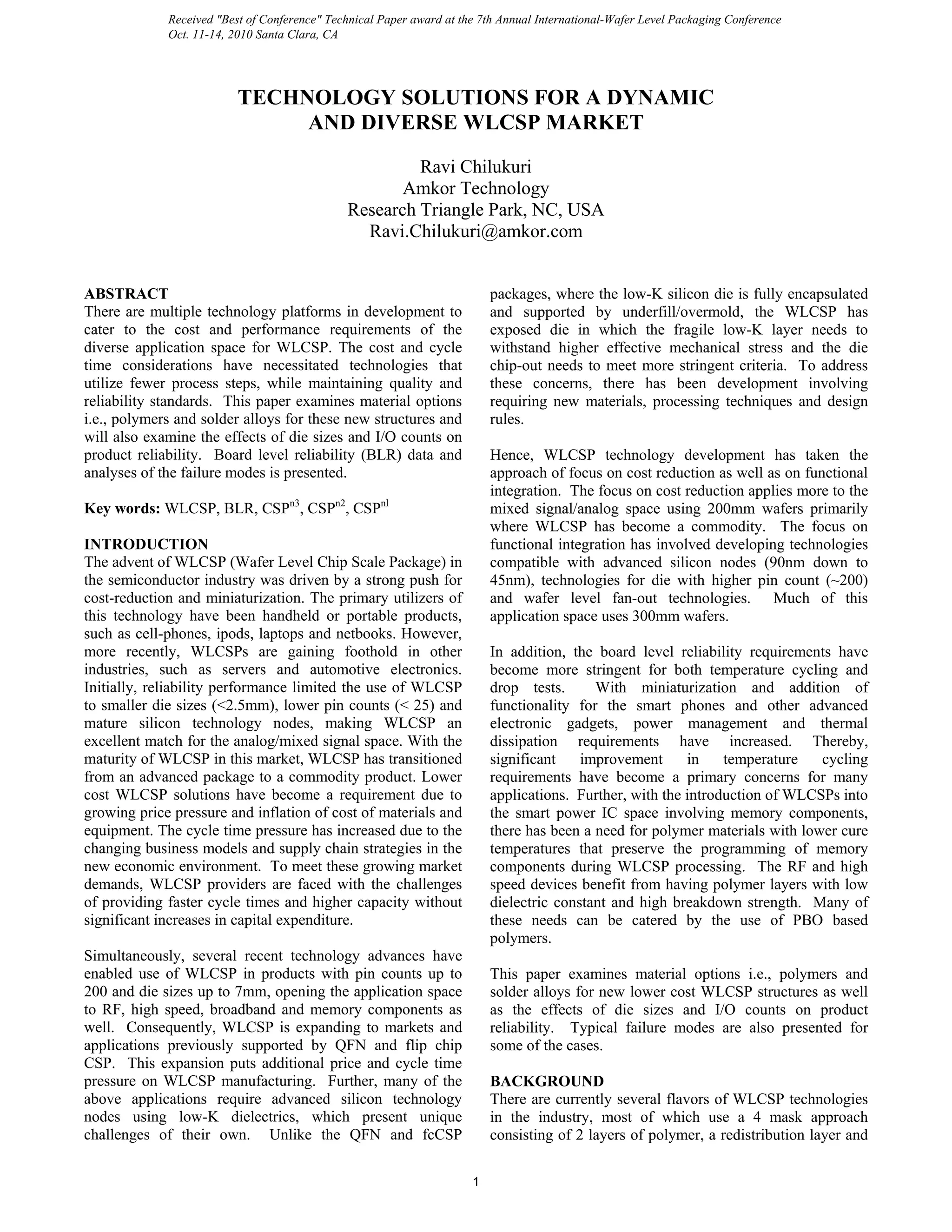
![a UBM (under bump metallurgy) under the solder bump,
similar to Amkor’s WLCSP offering, CSPnl
. As discussed
previously [10], the recent focus has been to develop cost
effective RDL based WLCSP options (CSPn3
and CSPn2
)
that are meet the reliability requirements for most WLCSP
applications. Both of these technologies are derivatives of
the current HVM offering of CSPnl
. A comparison of these
technologies is provided in Figure 1. Unlike CSPnl
, which
uses a 4 mask process, the CSPn3
is a three mask stack-up
that provides cost and cycle time savings through
elimination of process steps and lower material costs.
Further cost reduction can be realized through CSPn2
, where
the first polymer layer is left out of the device stack-up.
CSPnl
CSPn3
(CSPnl thick Cu UBM)
1) Polymer Coat 4) UBM
2) RDL 5) Ball Place
3) Polymer Coat
1) Polymer Coat
2) RDL/UBM 4) Ball Place
3) Polymer Coat
NO1st Polymer Coat
1) RDL/UBM 3) Ball Place
2) Polymer Coat
CSPn2
(CSPX3 minus Polymer 1)
Polyimide 2
Figure 1. Amkor WLCSP stack-up options: CSPnl
, CSPn3
and CSPn2
Early data demonstrated that the BLR (board level
reliability) performance of the above three technologies is
comparable [11] and meet the generally accepted guidelines
for reliability performance. CSPn3
has since been tested for
package level reliability using PBO, in addition to
Polyimide (PI). Extensive BLR studies have also been done
comparing PBO to PI on CSPn3
. Solder alloy comparisons
have been done using BLR on both CSPn3
and CSPn2
.
PACKAGE LEVEL RELIABILITY
The CSPn3
structure was built using PI for both the first and
second polymer levels. The die design used for the BLR
tests was a 5.5mm x 5.5mm die with a 10x10 full bump
array at 0.5mm pitch (Figure 2). The wafers were
background to 11mil silicon thickness prior to dicing the
parts. A number of package level reliability tests were
performed on these parts, as listed along with the passing
conditions in Table 1. All the parts were preconditioned at
MSL1 requirements. Parts were electrically and optically
tested prior to preconditioning, after preconditioning and
after reliability testing. Bump shears were also performed
following the reliability tests. The same process and tests
were repeated on parts built using PBO for both the first and
second polymer levels.
Table 1. Package level reliability tests performed on
Polyimide and PBO based CSPn3
structures.
TestItem Test/Pass Condition
Multiple Reflow 260C, 5X
Preconditioning at Level 1 85°C/85%, 168hrs, reflow @260°C peak
Preconditioning at Level 3 30°C/60%, 192hrs, reflow @260°C peak
Autoclave (PCT) 121C, 2 atm, 100% RH, 168 hrs
Unbiased HAST 130C, 85% RH, 168 hrs
Temp Cycle (TC) -55C/+125C, 1000 cycles
High Temp Storage (HTS) 150C, 1000 hrs
Figure 2. Die design used for package reliability tests:
10x10 I/O, 0.5mm pitch, 5.5mmx5.5mm, 0.3mm sphere.
PI VERSUS PBO BLR COMPARISON ON CSPn3
In addition to the package level reliability, board level
reliability (BLR) was also evaluated for PI based CSPn3
versus PBO based CSPn3
. The die design used for the BLR
tests was a 5.3mm x 5.3mm die with a 12x12 full bump
array at 0.4mm pitch (Figure 3). The solder alloy used was
SAC405.
Figure 3. Die design used for board level reliability tests:
12x12 I/O, 0.4mm pitch, 5.3mmx5.3mm, 0.25mm sphere.
For BLR, JEDEC drop test and thermal cycling were
evaluated. The drop test board was an 8 layer board, and
the thermal cycle board had 4 layers. The boards used were
NSMD with 250um diameter Cu pads.
The JEDEC thermal cycling condition used for this study
was JEDEC JESD22-A104C, Condition G [4]. Parts were
cycled between -40 to 125C at 1 cycle/hour. The
temperature ramp was 18min and the dwell time at
temperature was 12min. Three boards with 15 mounted
2
Received "Best of Conference" Technical Paper award at the 7th Annual International-Wafer Level Packaging Conference
Oct. 11-14, 2010 Santa Clara, CA](https://image.slidesharecdn.com/263098ab-743f-44ba-b220-15885a0438f8-160502005843/85/TechSolutionsWLCSPMarket-2-320.jpg)
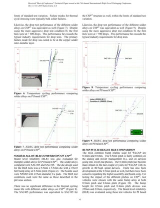
![WLCSP devices were used for each test case. The
comparison for PI based CSPn3
versus PBO based CSPn3
shows > 2X improvement in the mean life with the use of
PBO (Figure 4). With the PBO, mean life was greater than
1000 cycles for this 144 I/O die with first fails of greater
than 600 cycles. The failure modes for both the PI and PBO
versions were noted to be in bulk solder.
ReliaSoft W eibull++ 7 - www.ReliaSoft.com
Cycles to Failure
Cumulative%Failed
10 10000100 1000
1
5
10
50
90
99
PBO
CSPn3 PI
CSPn3 PBO
PI
Figure 4. Temperature cycling performance comparing PI
and PBO versions of CSPn3
.
The setup of the board level drop tester follows the
guidelines of JEDEC drop test standards [1-3], with 15
WLCSP devices (3x5 matrix) assembled on a test board
(132x77mm). The test board is connected to a fixture with
the die side facing down and then mounted to a drop block
with screws in the four corners of the PCB. This procedure
insures that the board experiences maximum flexure. The
drop block is dropped from a certain height along two
guiding rods, onto a rigid base covered with a rubber layer.
A multi-channel in-situ high speed data acquisition system
is used to measure input/output acceleration, in-plane strains
on board, and resistance of daisy-chained components. The
JEDEC drop test standard recommends certain input
acceleration values and pulse shapes [1-3]. The testing
described in this paper applied the aggressive JEDEC
condition H (2900G/0.3ms). The widely used JEDEC
condition B (1500G/0.5ms) proved to be impractical for
these parts due to the extensive testing time that would have
been required to collect sufficient data for statistical
analysis. Four boards per test case were utilized for drop
testing.
Drops to Failure
Cumulative%Failed
10.000 10000.000100.000 1000.000
1.000
5.000
10.000
50.000
90.000
99.000
PBO
PI
Jedec JESD22-B111
Condition H (2900G, 0.3ms)
Grp A
CSPn3 PI
CSPn3 PBO
Figure 5. JEDEC drop test performance comparing PI and
PBO versions of CSPn3
.
Previously, the drop performance of CSPn3
for both JEDEC
drop condition H (2900G/0.3ms) and condition B
(1500G/0.5ms) was compared [10]. From failure analysis,
the primary failure mode was found to be separation through
the IM at the Pb-free / Cu interface. The acceleration factor
between the two different drop conditions for this type of
IMC failure was 3X. Consequently, if the first failure (FF)
of a design under the condition H test conditions is 100,
then the FF under condition B would be estimated to be 300.
A comparison of the condition H drop test for PI versus
PBO shows no difference in the drop test performance
(Figure 5). For both cases, the mean life was > 1000 drops
at condition H indicating an expected life of about >3000
drops at the industry wide typically used condition B using
the above acceleration factor.
SOLDER ALLOY BLR COMPARISON ON CSPn3
Board level reliability (BLR) was also evaluated for
multiple solder alloys for PI based CSPn3
. The solder alloys
compared were SAC405, SAC105 and LF35. SAC405 was
selected for its higher silver content, which has typically
provided better TC performance than the lower silver
content alloys such as SAC105 on standard WLCSP stack-
ups. SAC105 was chosen due to the better drop test
performance that it has typically exhibited on standard
WLCSP stack-ups. LF35 was chosen due to the additional
dopant it contains that is expected to improve drop test
performance when the failures are in the IMC. The die
design used for the BLR tests was a 5.3mm x 5.3mm die
with a 12x12 full bump array at 0.4mm pitch (Figure 3).
The boards used were NSMD with 250um diameter Cu
pads. The BLR test conditions used were the same as those
described in the previous section.
There was no significant difference in the thermal cycling
mean life with different solder alloys on CSPn3
(Figure 6).
The plots for SAC105 and LF35 overlapped, as may be
expected due to the similar silver content in these two
alloys. Interestingly, the SAC405 performance was
equivalent to SAC105 for the CSPn3
structure, within the
3
Received "Best of Conference" Technical Paper award at the 7th Annual International-Wafer Level Packaging Conference
Oct. 11-14, 2010 Santa Clara, CA](https://image.slidesharecdn.com/263098ab-743f-44ba-b220-15885a0438f8-160502005843/85/TechSolutionsWLCSPMarket-3-320.jpg)
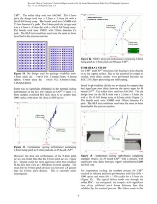
![case was separation of the solder bump from the copper
trace at the copper – IMC interface.
For the drop test, the standard process for CSPn3
resulted in
excellent performance with first fails > 600 drops and mean
life > 1500 drops, using the more aggressive drop test
condition H (Figure 14). This performance far exceeds the
typical industry requirements for drop tests. The typical
failure mode was through the bulk solder, as typically
observed for temperature cycling. As anticipated, the
samples with significant time delay exhibited much lower
lifetimes than that exhibited by the standard process. The
failure mode in this case was separation of the solder bump
from the copper trace at the copper – IMC interface.
ReliaSoft Weibull++ 7 - www.ReliaSoft.com
Drops to Failure
Cumulative%Failed
1 1000010 100 1000
1
5
10
50
90
99
With Delay
Standard Process
Figure 14. JEDEC drop test performance comparing
standard process on PI based CSPn3
with a process with
significant time delay between copper redistribution/UBM
and ball load.
CONCLUSIONS
The BLR drop and thermal cycling data for CSPn3
and
CSPn2
position these technologies as cost effective and
viable WLCSP options. A comparison of PBO and PI based
CSPn3
technologies exhibited >2X improvement in thermal
cycling life and comparable drop performance using PBO.
With different solder alloys, CSPn3
exhibited equivalent TC
and drop performance. The 0.4mm and 0.5mm pitch
devices showed equivalent TC performance. Processing
time delay between UBM and ball load demonstrated to be
significant for package reliability.
ACKNOWLEDGEMENTS
Appreciation is extended to our colleagues from the R&D
group of Amkor Korea: SS Park, ES Yang, DH Moon, SW
Cha, TK Hwang and WJ Kang, as well as former
colleagues, Rex Anderson and Boyd Rogers, for their
technical support and efforts.
REFERENCES
[1] JEDEC Standard JESD22-B111, Board Level Drop Test
Method of Components for Handheld Electronic
Products, 2003.
[2] JEDEC Standard JESD22-B104-B, Mechanical Shock,
2001.
[3] JEDEC Standard JESD22-B110, Subassembly
Mechanical Shock, 2001.
[4] JEDEC Standard JESD22-A104C, Temperature Cycling,
2005.
[5] R. Anderson, T.Y. Tee, R. Chilukuri, H.S. NG, C.P.
Koo, and B. Rogers, “Amkor’s CSPnlTM
: Comparison of
Bump on Pad and Cu Redistribution WLCSP Designs",
IMAPS Proc., Scottsdale, AZ, (2009).
[6] T.Y. Tee, H.S. Ng, A. Syed, R. Anderson, C.P. Khoo, B.
Rogers “Design for Board Trace Reliability of WLCSP
under Drop Test”, 10th Eurosime Conference,
Netherlands, (2009).
[7] T.Y. Tee, L.B. Tan, R. Anderson, H.S. Ng, J.H. Low,
C.P. Khoo, R. Moody, B. Rogers, “Advanced Analysis
of WLCSP Copper Interconnect Reliability under Board
Level Drop Test”, EPTC Proc, Singapore, 1086-1095
(2008).
[8] R. Anderson, T.Y. Tee, R. Moody, L.B. Tan, H.S. NG,
J.H. Low, and B. Rogers, “Integrated Testing &
Modeling Analysis of CSPnl™ for Enhanced Board
Level Reliability”, IWLPC Proc., San Jose, CA, 184-
190, (2008).
[9] R. Anderson, Robert Moody, Boyd Rogers, and Dan
Mis, “Board Level Reliability Results for Amkor’s
12x12 I/O CSPnl™”, IMAPS Proc., Scottsdale, AZ
(2008).
[10] R. Anderson, R. Chilukuri, T.Y. Tee, C.P. Koo, H.S.
NG, B. Rogers, and A. Syed, “ Advances in WLCSP
technologies for growing market needs”, IWLPC Proc.,
San Jose, CA (2009).
[11] R. Anderson, R. Chilukuri, B. Rogers, and A. Syed, “
Advances in WLCSP technologies to enable cost
reduction”, IMAPS Proc., Scottsdale, AZ (2010).
6
Received "Best of Conference" Technical Paper award at the 7th Annual International-Wafer Level Packaging Conference
Oct. 11-14, 2010 Santa Clara, CA](https://image.slidesharecdn.com/263098ab-743f-44ba-b220-15885a0438f8-160502005843/85/TechSolutionsWLCSPMarket-6-320.jpg)


