Subprograms and Memory
Modelingusing VHDL
Dr. Shubhajit Roy Chowdhury,
School of Computing and Electrical Engineering,
Indian Institute of Technology Mandi, India
Email: src@iitmandi.ac.in
SCEE, IIT MANDI
Dr. Shubhajit Roy Chowdhury
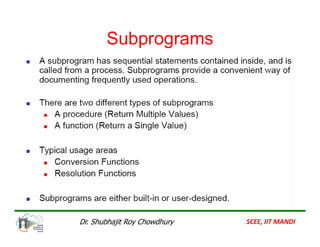
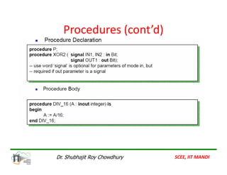
Subprograms (cont’d)
• Containsequential statements similar to processes
• May declare local variables, constants
• Executed when called from a sequential statement.
• Local Variables are re-initialized every time a subprogram is called.
• Parameters of calling routine are known as actuals, while the parameters of the
declared subprogram are known as formals.
• Up level referencing to higher level variables and signals is allowed.
• Recursive calls by functions and procedures are allowed
• Attributes of signals cannot be accessed within subprograms
SCEE, IIT MANDI
Dr. Shubhajit Roy Chowdhury
4.
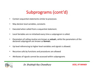
Functions
• Produce asingle return value
• Called by expressions
• Cannot modify the parameters passed to them
• Require a RETURN statement
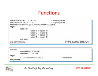
FUNCTION add_bits (a, b : IN BIT) RETURN BIT IS
BEGIN -- functions cannot return multiple values
FUNCTION add_bits2 (a, b : IN BIT) RETURN BIT IS
VARIABLE result : BIT; -- variable is local to function
BEGIN
result := (a XOR b);
RETURN result; -- the two functions are equivalent
END add_bits2;
BEGIN -- functions cannot return multiple values
RETURN (a XOR b);
END add_bits;
SCEE, IIT MANDI
Dr. Shubhajit Roy Chowdhury
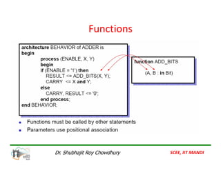
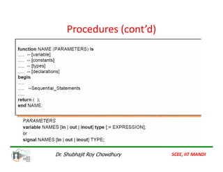
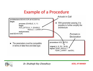
Example of aProcedure
SCEE, IIT MANDI
Dr. Shubhajit Roy Chowdhury
11.
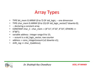
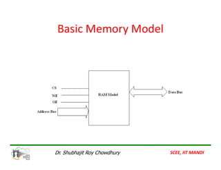
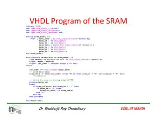
Array Types
• TYPEbit_mem IS ARRAY (0 to 7) OF std_logic; -- one dimension
• TYPE char_mem IS ARRAY (0 to 15) OF std_logic_vector(7 downto 0);
• -- declaring a constant array
• CONSTANT char_1 : char_mem := (X”11”, X”22”, X”33”, OTHERS =>
• X”00”);
• variable address : integer range 0 to 15;
-- vcount is a std_logic_vector, row counter
• -- vcount is a std_logic_vector, row counter
• address := conv_integer(vcount (v2 downto v1);
• shift_reg <= char_1(address);
SCEE, IIT MANDI
Dr. Shubhajit Roy Chowdhury
12.
Array Types
• TYPEbit_mem IS ARRAY (0 to 7) OF std_logic; -- one dimension
• TYPE char_mem IS ARRAY (0 to 15) OF std_logic_vector(7 downto 0);
• -- declaring a constant array
• CONSTANT char_1 : char_mem := (X”11”, X”22”, X”33”, OTHERS =>
• X”00”);
• variable address : integer range 0 to 15;
-- vcount is a std_logic_vector, row counter
• -- vcount is a std_logic_vector, row counter
• address := conv_integer(vcount (v2 downto v1);
• shift_reg <= char_1(address);
SCEE, IIT MANDI
Dr. Shubhajit Roy Chowdhury
13.
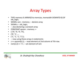
Array Types
• TYPEmemory IS ARRAY(0 to memsize, memwidth DOWNTO 0) OF
std_logic;
• SIGNAL ram : memory; -- declare array
• SIGNAL z : std_logic;
• -- also declaring a constant array
• CONSTANT eprom : memory :=
• ( (‘0’, ‘0’, ‘0’, ‘0’),
• ( (‘0’, ‘0’, ‘0’, ‘0’),
• (‘0’, ‘1’, ….
• (‘1’, ‘1’, ‘1’, ‘1’) );
• -- now using these arrays in statements
• z <= eprom(6,1); -- read element at 2nd column of 7th row.
• ram(2,3) <= ‘1’; -- set element of ram
SCEE, IIT MANDI
Dr. Shubhajit Roy Chowdhury
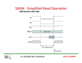
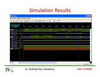
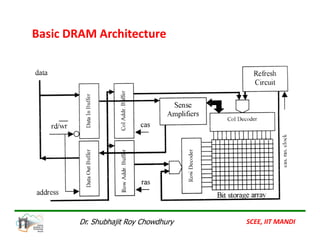
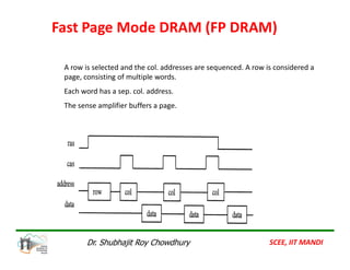
Fast Page ModeDRAM (FP DRAM)
A row is selected and the col. addresses are sequenced. A row is considered a
page, consisting of multiple words.
Each word has a sep. col. address.
The sense amplifier buffers a page.
SCEE, IIT MANDI
Dr. Shubhajit Roy Chowdhury
21.
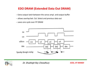
EDO DRAM (ExtendedData Out DRAM)
-- Extra output latch between the sense ampl. and output buffer
-- allows overlap bet. Col. Select and previous data out
-- saves one cycle over FP DRAM
SCEE, IIT MANDI
Dr. Shubhajit Roy Chowdhury
22.
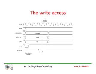
•FPM and EDORAM controlled asynchronously by the processor or the
memory controller.
•A synchronous DRAM interface will eliminate a small amount of time
(thus latency) that is needed by the DRAM to detect the ras/cas and
rd/wr signals. DRAM latches information to and from the controller on
the active edge of the clock signal
•In addition to a lower latency I/O, after a proper page and column
SDRAM
•In addition to a lower latency I/O, after a proper page and column
setup, an SDRAM may store the starting address internally and output
new data on each active edge of the clock signal, as long as the
requested data are consecutive memory locations. This is accomplished
by adding a column address counter to the base DRAM architecture.
This counter is seeded with a starting column address strobed in by the
processor (or memory controller) and is thereafter incremented
internally by the DRAM on each clock cycle.
SCEE, IIT MANDI
Dr. Shubhajit Roy Chowdhury
23.
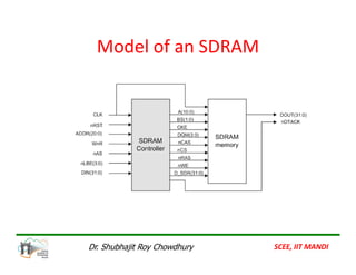
Model of anSDRAM
SCEE, IIT MANDI
Dr. Shubhajit Roy Chowdhury
24.
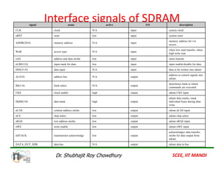
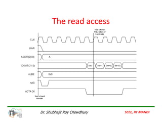
Interface signals ofSDRAM
signal name active I/O description
CLK clock N/A input system clock
nRST reset low input system reset
ADDR(20:0) memory address N/A input
memory address for r/w
access
WnR access type N/A input
when low read transfer, when
high write tran.
nAS address and data strobe low input starts transfer
nLBE(3:0) input mask for data low input input enable/disable for data
DIN(31:0) data input N/A input data to be written into sdram
A(10:0) address bus N/A output
address or control signals into
sdram
BS(1:0) bank select N/A output
determines bank to which
commands are executed
BS(1:0) bank select N/A output
commands are executed
CKE clock enable high output sdram CKE input
DQM(3:0) data mask high output
sdram data masks, mask
individual bytes during data
write.
nCAS column address strobe low output sdram nCAS input
nCS chip select low output sdram chip select
nRAS row address strobe low output sdram nRAS input
nWE write enable low output sdram nWE input
nDTACK transmission acknowledge low output
acknowledges data transfer,
strobe for data output from
sdram
DATA_OUT_SDR data bus N/A output sdram data in bus
SCEE, IIT MANDI
Dr. Shubhajit Roy Chowdhury