Basics of ComputerSystems
• Computer is a programmable machine.
• Computer is a machine that manipulates data according to a list of instructions.
• Computer is any device which aids humans in performing various kinds of
computations or calculations.
Three principle characteristics of computer
• It responds to a specific set of instructions in a well-defined manner.
• It can execute a pre-recorded list of instructions.
• It can quickly store and retrieve large amounts of data.
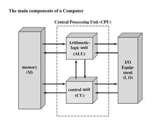
Input Unit
• Computersaccept coded information through input units.
• The most common input device is the keyboard. Whenever a key is pressed, the
corresponding letter or digit is automatically translated into its corresponding
binary code and transmitted to the processor.
• Many other kinds of input devices are available, including the touchpad, mouse,
joystick, and trackball. These are often used as graphic input devices in
conjunction with displays.
• Microphones can be used to capture audio input which is then sampled and
converted into digital codes for storage and processing.
• Similarly, cameras can be used to capture video input.
• Digital communication facilities, such as the Internet, can also provide input to a
computer from other computers and database servers.
6.
Output Unit
• Theoutput unit is the counterpart of the input unit.
• Its function is to send processed results to the outside world. A familiar example
of such a device is a printer.
• However, printers are mechanical devices, and as such are quite slow compared
to the electronic speed of a processor.
• Some units, such as graphic displays, provide both an output function, showing
text and
• graphics, and an input function, through touch-screen capability.
• The dual role of such units is the reason for using the single name input/output
(I/O) unit in many cases.
7.
Central Processing Unit(CPU)
1. Arithmetic and Logic Unit (ALU)
• Computer operations are executed in the arithmetic and logic unit (ALU) of the
processor.
• Any arithmetic or logic operation, such as addition, subtraction, multiplication,
division, or comparison of numbers, is initiated by bringing the required
operands into the processor, where the operation is performed by the ALU.
• When operands are brought into the processor, they are stored in high-speed
storage elements called registers.
• Each register can store one word of data. Access times to registers are even
shorter than access times to the cache unit on the processor chip.
8.
Central Processing Unit(CPU)
2. Control Unit (CU)
• The memory, arithmetic and logic unit, and I/O units store and process
information and perform input and output operations.
• The operation of these units must be coordinated in some way. This is the
responsibility of the control unit.
• The control unit sends control signals to other units and senses their states.
• Control circuits are responsible for generating the timing signals that govern the
transfers and determine when a given action is to take place.
• Data transfers between the processor and the memory are also managed by the
CU
• A large set of control lines (wires) carries the signals used for timing and
synchronization of events in all units.
9.
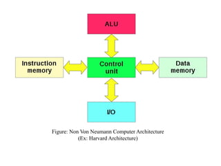
The Von Neumannand Non Von Neumann Model
The Von Neumann Model
• It is also known as the von Neumann model or Princeton architecture
• Introduced by John Von Neumann in 1945
• A processing unit with an arithmetic logic unit, control unit, and processor
registers
• The control unit includes an instruction register and a program counter
• It has same memory that stores data and instructions
• The mass storage is used separately/externally
• It refer to a stored-program computer in which an instruction fetch and a data
operation cannot occur at the same time (since they share a common bus).
• This problem is referred to as the von Neumann bottleneck problem, which
overall slower the computer processing
The Von Neumannand Non Von Neumann Model
The Non Von Neumann Model
• Any computer architecture having separate pathways for transferring data and
instructions come under the category of Non Von Neumann model
• It has separate memories for storing data and instructions
• This architecture include multiple bus system for transferring instructions and
data separately
• As the data and instructions can be operated separately and simultaneously
hence, multiple steps can be solved by the computer in fewer clock cycles
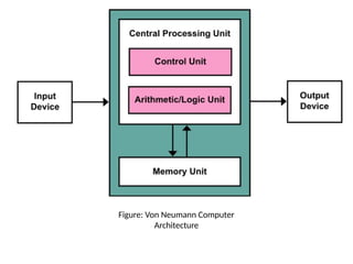
12.
Figure: Non VonNeumann Computer Architecture
(Ex: Harvard Architecture)
13.
Comparison of TheVon Neumann and Non Von Neumann Model
Parameter Von Neumann Model Non Von Neumann Model
Memory
arrangement
Instruction and Data both
are stored in same memory
It contains separate memory for
storing Instruction and Data
Bus
arrangement
It has single bus to transfer
instruction and Data hence
transferred sequentially
It has multiple buses connected to
instruction memory and Data
memory separately, hence
instructions and data can be
transferred
simultaneously/parallelly
Speed of
execution
As instruction and data are
sent sequentially over a
single bus speed of
execution is slower
As instruction and data are sent
parallelly over a multiple buses
speed of execution is Faster
Clock cycle
(instruction
execution
contains
multiple steps)
More clock cycles for single
instruction
Less clock cycles (or mostly one
clock cycle) for single instruction
14.
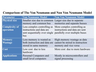
Comparison of TheVon Neumann and Non Von Neumann Model
Parameter Von Neumann Model Non Von Neumann Model
Physical size Smaller size due to common
memory and common bus
Larger size due to separate
memories and separate busses
Complexity of
operation
Less complex controlling as
instructions and data are
sent sequentially over single
bus
More complex controlling as
instructions and data are sent
parallelly over multiple buses
Memory
Wastage
Less memory is wasted as
both instruction and data are
stored in same memory
High memory wastage as data
cannot be stored in instruction
memory and vice versa
Cost Low cost due to less
hardware
More cost due to more hardware
Applications Personal Computers and
small level computers
Mostly in microcontrollers and
signal processing
15.
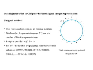
Data Representation inComputer Systems: Signed Integer Representation
Circle representation of unsigned
integers mod N
Unsigned numbers
• This representation contains all positive numbers
• Total number for presentations are 2n
(Here n is
number of bits for representation)
• Range is specified as (0 2n
- 1)
• For n=4 the number are presented with their decimal
values are 0000(0), 0001(1), 0010(2), 0011(3),
0100(4),......,1110(14), 1111(15)
16.
Data Representation inComputer Systems: Signed Integer Representation
Mod 16 system for 2’s-
complement numbers
Signed numbers
• Total number for presentations are 2n
(Here n is number of bits for
representation)
• This representation contains half
positive numbers and half negative
numbers
• Range is specified in two categories
• Positive Range [0 (2n
/2 - 1)]
• Negative Range [- 2n
/2 - 1]
17.
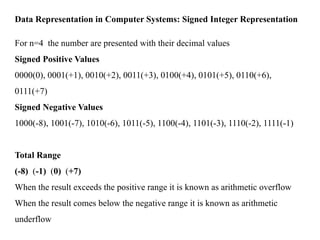
Data Representation inComputer Systems: Signed Integer Representation
For n=4 the number are presented with their decimal values
Signed Positive Values
0000(0), 0001(+1), 0010(+2), 0011(+3), 0100(+4), 0101(+5), 0110(+6),
0111(+7)
Signed Negative Values
1000(-8), 1001(-7), 1010(-6), 1011(-5), 1100(-4), 1101(-3), 1110(-2), 1111(-1)
Total Range
(-8) (-1) (0) (+7)
When the result exceeds the positive range it is known as arithmetic overflow
When the result comes below the negative range it is known as arithmetic
underflow
18.
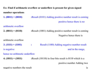
Ex: Find ifarithmetic overflow or underflow is present for given signed
number operations
1. (0011) + (0010) :Result (0101) Adding positive number result is coming
positive hence there is no
arithmetic overflow
2. (0011) + (0110) :Result (1001) Adding positive number result is coming
Negative hence there is
arithmetic overflow
3. (1111) + (1101) : Result (1100) Adding negative number result
is negative and in the range,
hence no arithmetic underflow
4. (1011) + (1011) :Result (10110) in four bits result is 0110 which is a
positive number Adding two
negative numbers the result is
19.
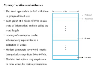
Memory Locations andAddresses
• The usual approach is to deal with them
in groups of fixed size.
• Each group of n bits is referred to as a
word of information, and n is called the
word length.
• memory of a computer can be
schematically represented as a
collection of words
• Modern computers have word lengths
that typically range from 16 to 64 bits.
• Machine instructions may require one
or more words for their representation.
20.
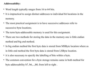
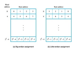
Addressability:
• Word lengthtypically ranges from 16 to 64 bits.
• It is impractical to assign distinct addresses to individual bit locations in the
memory.
• The most practical assignment is to have successive addresses refer to
successive byte locations.
• The term byte-addressable memory is used for this assignment.
• There are two methods for storing the data in the memory one is little endian
method and big end method.
• In big endian method the first byte data is stored from MSByte location where as
in little end method the first byte data is stored from LSByte location.
• it is also necessary to specify the labelling of bits within a byte.
• The common convention for a byte storage remains same in both method for
byte addressability b7, b6,...,b0, from left to right .
22.
Word Alignment:
• Naturalword boundaries occur at addresses 0, 4, 8, . . .
• The word locations have aligned addresses if they begin at a byte address that is
a multiple of the number of bytes in a word.
• There is no fundamental reason why words cannot begin at an arbitrary byte
address.
• The most common case is to use aligned addresses, which makes accessing of
memory operands more efficient
23.
Memory Locations andAddresses
Question: Consider a data which needs to be stored in the byte addressability
format for a memory with word length of 32-bit.
0X1A2B3C4D5E6F0784
Represent the given number in byte addressability with both big end and little end
method.
Answer:
A 32-bit word length memory will be able to manage 4 bytes of data in a single
word
The current data needs to be stored in the memory is in hexadecimal
representation
hence the bytes will be [1A], [2B], [3C], [4D], [5E], [6F], [07], [84]
24.
Memory Locations andAddresses
Big-End method Byte addressability
Representation will be as follows
In byte addressability 8-bit data go together
In Hexadecimal:
Word 1: [1A] [2B] [3C] [4D]
Word 2: [5E] [6F] [07] [84]
In Binary:
Word 1: [0001 1010] [0010 1011] [0011 1100] [0100
1101]
Word 2: [0101 1110] [0110 1111] [0000 0111] [1000
0100]
25.
Memory Locations andAddresses
Little-End method Byte addressability
Representation will be as follows
In byte addressability 8-bit data go together
In Hexadecimal:
Word 1: [4D] [3C] [2B] [1A]
Word 2: [84] [07] [6F] [5E]
In Binary:
Word 1: [0100 1101] [0011 1100] [0010 1011] [0001
1010]
Word 2: [1000 0100] [0000 0111] [0110 1111] [0101
1110]
26.
Instruction Notations:
• Thetasks carried out by a computer program consist of a sequence of small
steps, such as adding two numbers, testing for a particular condition, reading a
character from the keyboard, or sending a character to be displayed on a display
screen.
• A computer must have instructions capable of performing four types of
operations:
1. Data transfers between the memory and the processor registers
2. Arithmetic and logic operations on data
3. Program sequencing and control
4. I/O transfers
27.
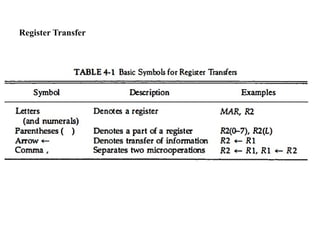
Register Transfer Language/Notations:
•Used to describe the transfer of information from one location to another.
• Possible transfers are memory locations, processor registers, or registers in the
I/O subsystem
• It has some sources and destination
a. Memory to Register Transfer
In this the data is transferred from some place in memory/location/local variable to
a processor register. The notation is described
R2 ← [LOC]
b. Register to Register Transfer
R4 ← [R2] + [R3]
c. Memory to I/O Device
R4 ← [Input Device]
[OUT STATUS] ← R4
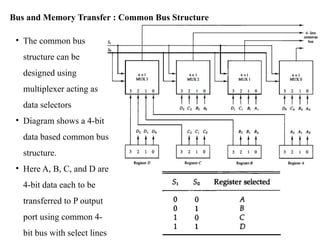
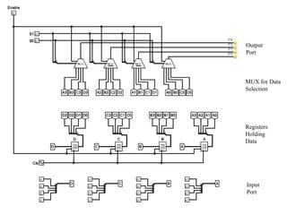
• The commonbus
structure can be
designed using
multiplexer acting as
data selectors
• Diagram shows a 4-bit
data based common bus
structure.
• Here A, B, C, and D are
4-bit data each to be
transferred to P output
port using common 4-
bit bus with select lines
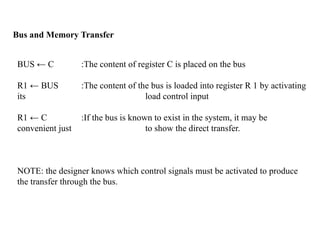
Bus and Memory Transfer : Common Bus Structure
Bus and MemoryTransfer
BUS ← C :The content of register C is placed on the bus
R1 ← BUS :The content of the bus is loaded into register R 1 by activating
its load control input
R1 ← C :If the bus is known to exist in the system, it may be
convenient just to show the direct transfer.
NOTE: the designer knows which control signals must be activated to produce
the transfer through the bus.
32.
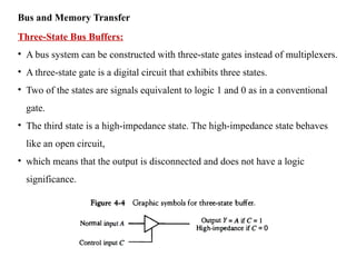
Bus and MemoryTransfer
Three-State Bus Buffers:
• A bus system can be constructed with three-state gates instead of multiplexers.
• A three-state gate is a digital circuit that exhibits three states.
• Two of the states are signals equivalent to logic 1 and 0 as in a conventional
gate.
• The third state is a high-impedance state. The high-impedance state behaves
like an open circuit,
• which means that the output is disconnected and does not have a logic
significance.
33.
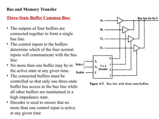
Bus and MemoryTransfer
Three-State Buffer Common Bus:
• The outputs of four buffers are
connected together to form a single
bus line.
• The control inputs to the buffers
determine which of the four normal
inputs will communicate with the bus
line
• No more than one buffer may be in
the active state at any given time.
• The connected buffers must be
controlled so that only one three-state
buffer has access to the bus line while
all other buffers are maintained in a
high impedance state.
• Decoder is used to ensure that no
more than one control input is active
at any given time
34.
Bus and MemoryTransfer
Memory Transfer:
The transfer of information from a memory word to the outside environment is
called a read operation.
The transfer of new information to be stored into the memory is called a write
operation.
Memory Read: DR ← M[AR]
Memory Write: R3 ← R1 + R2’ + 1
Here
DR – Data Register
AR – Address Register
M – Memory
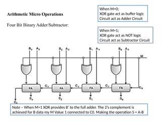
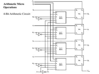
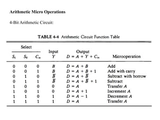
Arithmetic Micro Operations
FourBit Binary Adder/Subtractor:
When M=0;
XOR gate act as buffer logic
Circuit act as Adder Circuit
When M=1;
XOR gate act as NOT logic
Circuit act as Subtractor Circuit
Note – When M=1 XOR provides B’ to the full adder. The 2’s complement is
achieved for B data my M Value 1 connected to C0. Making the operation S = A-B
38.
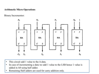
Arithmetic Micro Operations
BinaryIncrementor:
• This circuit add 1 value to the A data.
• In case of incrementing a data we add 1 value to the LSB hence 1 value is
added in A0 using half adder.
• Remaining Half adders are used for carry addition only.
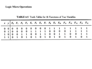
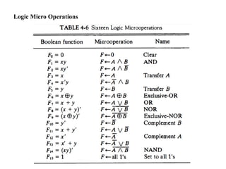
Logic Micro Operations
Logicmicrooperations specify binary operations for strings of bits stored in
registers. These operations consider each bit of the register separately and treat
them as binary variables.
P: R1 ← R1 R2
⊕
1010 : Content of R1
1100 : Content of R2
0110 : After P=1; Content of R1
42.
Logic Micro Operations
•The symbol ˅ will be used to denote an OR microoperation
• the symbol ˄ to denote an AND microoperation.
• The complement microoperation is the same as the 1's complement and uses a bar
• on top of the symbol that denotes the register name.
P + Q: R 1 ← R2 + R3
R4 ← R5 V R6
The + between P and Q is an OR operation between two binary variables of a
control function. The + between R2 and R3 specifies an add microoperation.
The OR microoperation is designated by the symbol V between registers R5
and R6.
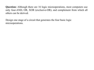
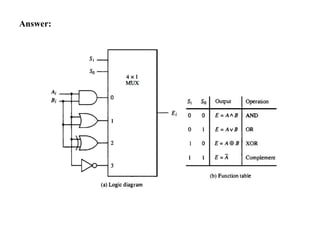
Question: Although thereare 16 logic microoperations, most computers use
only four-AND, OR, XOR (exclusive-OR), and complement from which all
others can be derived.
Design one stage of a circuit that generates the four basic logic
microoperations.
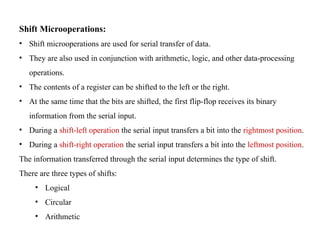
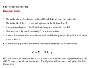
Shift Microoperations:
• Shiftmicrooperations are used for serial transfer of data.
• They are also used in conjunction with arithmetic, logic, and other data-processing
operations.
• The contents of a register can be shifted to the left or the right.
• At the same time that the bits are shifted, the first flip-flop receives its binary
information from the serial input.
• During a shift-left operation the serial input transfers a bit into the rightmost position.
• During a shift-right operation the serial input transfers a bit into the leftmost position.
The information transferred through the serial input determines the type of shift.
There are three types of shifts:
• Logical
• Circular
• Arithmetic
48.
Shift Microoperations:
Logical ShiftOperation
• A logical shift is one that transfers 0 through the serial input.
• The symbols shl and shr are used for logical shift-left and shift-right microoperations
R1 ← shl R1
R2 ← shr R2
Bit transferred to the end position through the serial input is assumed to be 0 during logical shift
Logical Left Shift Operation
1 0 1 1 0 0 1 1 R1 – Before Shift Operation
0 1 1 0 0 1 1 R1 – During Logical Left Shift (shl)
0 1 1 0 0 1 1 R1 – After Logical Left Shift (shl)
0
49.
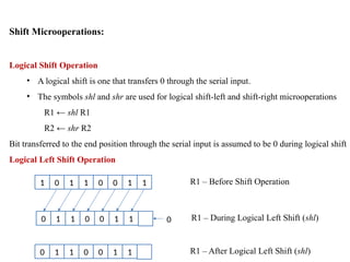
Logical Right ShiftOperation
1 0 1 1 0 0 1 1 R1 – Before Shift Operation
1 0 1 1 0 0 1 R1 – During Logical Right Shift (shr)
0 1 0 1 1 0 0 1 R1 – After Logical Right Shift (shr)
0
50.
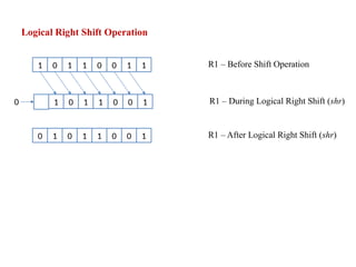
Shift Microoperations:
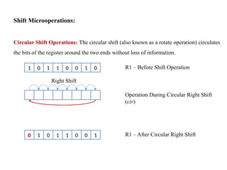
Circular ShiftOperations: The circular shift (also known as a rotate operation) circulates
the bits of the register around the two ends without loss of information.
1 0 1 1 0 0 1 0 R1 – Before Shift Operation
Operation During Circular Left Shift (cil)
0 1 1 0 0 1 0 1 R1 – After Circular Left Shift
Left Shift
51.
Shift Microoperations:
Circular ShiftOperations: The circular shift (also known as a rotate operation) circulates
the bits of the register around the two ends without loss of information.
1 0 1 1 0 0 1 0 R1 – Before Shift Operation
Operation During Circular Right Shift
(cir)
0 1 0 1 1 0 0 1 R1 – After Circular Right Shift
Right Shift
52.
Shift Microoperations:
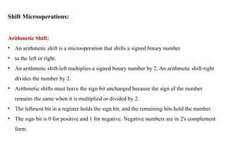
Arithmetic Shift:
•An arithmetic shift is a microoperation that shifts a signed binary number
• to the left or right.
• An arithmetic shift-left multiplies a signed binary number by 2. An arithmetic shift-right
divides the number by 2.
• Arithmetic shifts must leave the sign bit unchanged because the sign of the number
remains the same when it is multiplied or divided by 2.
• The leftmost bit in a register holds the sign bit, and the remaining bits hold the number.
• The sign bit is 0 for positive and 1 for negative. Negative numbers are in 2's complement
form.
53.
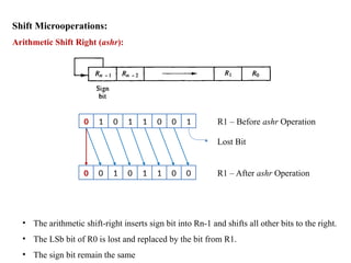
Shift Microoperations:
Arithmetic ShiftRight (ashr):
0 1 0 1 1 0 0 1 R1 – Before ashr Operation
0 0 1 0 1 1 0 0 R1 – After ashr Operation
Lost Bit
• The arithmetic shift-right inserts sign bit into Rn-1 and shifts all other bits to the right.
• The LSb bit of R0 is lost and replaced by the bit from R1.
• The sign bit remain the same
54.
Shift Microoperations:
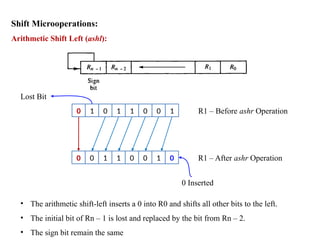
Arithmetic ShiftLeft (ashl):
0 1 0 1 1 0 0 1 R1 – Before ashr Operation
0 0 1 1 0 0 1 0 R1 – After ashr Operation
Lost Bit
0 Inserted
• The arithmetic shift-left inserts a 0 into R0 and shifts all other bits to the left.
• The initial bit of Rn – 1 is lost and replaced by the bit from Rn – 2.
• The sign bit remain the same
55.
Shift Microoperations:
Important Points
•The arithmetic shift-left inserts a 0 into R0 and shifts all other bits to the left.
• The initial bit of Rn – 1 is lost and replaced by the bit from Rn – 2.
• A sign reversal occurs if the bit in Rn-1 changes in value after the shift.
• This happens if the multiplication by 2 causes an overflow.
• An overflow occurs after an arithmetic shift left if initially, before the shift, Rn – 1 is not
equal to Rn – 2.
• An overflow flip-flop V, can be used to detect an arithmetic shift-left overflow.
If V, = 0, there is no overflow, but if V, = I, there is an overflow and a sign reversal after the
shift. V, must be transferred into the overflow flip-flop with the same clock pulse that shifts
the register.
57.
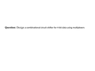
Question: Design acombinational circuit shifter for 4-bit data using multiplexers
58.
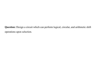
Question: Design acircuit which can perform logical, circular, and arithmetic shift
operations upon selection.
59.
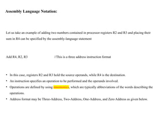
Assembly Language Notation:
Letus take an example of adding two numbers contained in processor registers R2 and R3 and placing their
sum in R4 can be specified by the assembly-language statement
Add R4, R2, R3 //This is a three address instruction format
• In this case, registers R2 and R3 hold the source operands, while R4 is the destination.
• An instruction specifies an operation to be performed and the operands involved.
• Operations are defined by using mnemonics, which are typically abbreviations of the words describing the
operations.
• Address format may be Three-Address, Two-Address, One-Address, and Zero Address as given below.
Instruction Formats
Two-Address Instructions
EvaluateX = (A + B) * (C + D) using Two-Address instructions
MOV R1, A // R1 ← M[A]
ADD R1, B // R1 ← R1 + M[B]
MOV R2, C // R2 ← M[C]
ADD R2, D // R2 ← R2 + M[D]
MUL R1, R2 // R1 ← R1 * R2
MOV X, R1 // M[X] ← R1
62.
Instruction Formats
One-Address Instructions
Usean implied AC register for all data manipulation
Evaluate X = (A + B) * (C + D) using One-Address instructions
LOAD A AC ← M[A]
ADD B AC ← AC + M[B]
STORE T M[T] ← AC
LOAD C AC ← M[C]
ADD D AC ← AC + M[D]
MUL T AC ← AC * M[T]
STORE X M[X] ← AC
Here AC is accumulator
63.
Instruction Formats
Zero-Address Instructions
EvaluateX = (A + B) * (C + D) using One-Address instructions
PUSH A TOS ← A
PUSH B TOS ← B
ADD TOS ← (A + B)
PUSH C TOS ← C
PUSH D TOS ← D
ADD TOS ← (C + D)
MUL TOS ← (C + D) * (A + B)
POP X M[X] ← TOS
TOS – Top of Stack
64.
Instruction Formats: ReversePolish Notation
The best way to write zero address program is using reverse polish notation.
For arithmetic expressions: A + B
A + B is a Infix notation
+ A B is a Prefix or Polish notation
A B + is a Postfix or reverse Polish notation
The reverse Polish notation is very suitable for stack manipulation
e.g. A * B + C * D can be written as = AB * CD * +
65.
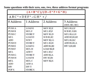
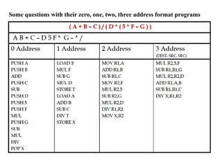
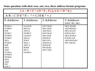
Questions on reversepolish notation for writing program in zero address format.
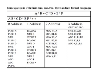
Give Zero, one, two and three address programs for given equations:
Q1: A * B + C * D + E * F
Ans: AB*CD*EF*+ +
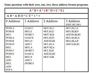
Q2: A * B + A * (B * D + C * E)
Ans: AB*ABD*CE*+*+
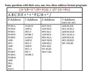
Q3: [ A * [ B + C * ( D + E ) ] ] / [ F * ( G + H ) ]
Ans: ABCDE+*+*FGH+*/
66.
Find the ReversePolish Notation:
Do the following question by yourself
Q4. (A + B * C) / (D – E * F + G * H)
Q5. A + B * [C * D + E * (F + G)]
Q6. (A + B – C) / (D * (5 * F – G))
Q7. (A – B + C * (D * E – F)) / (G + H * K)
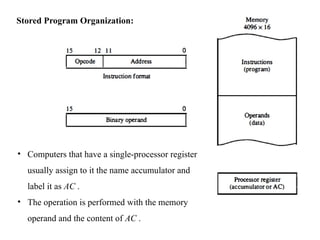
Stored Program Organization:
•Computers that have a single-processor register
usually assign to it the name accumulator and
label it as AC .
• The operation is performed with the memory
operand and the content of AC .
74.
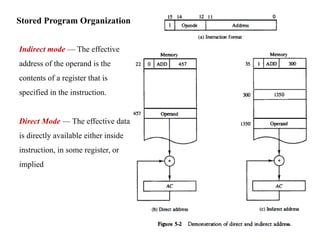
Stored Program Organization:
Indirectmode — The effective
address of the operand is the
contents of a register that is
specified in the instruction.
Direct Mode — The effective data
is directly available either inside
instruction, in some register, or
implied
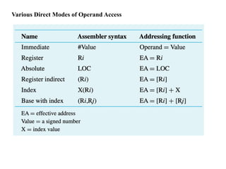
Various Direct Modesof Operand Access
Immediate mode
The operand is given explicitly in the instruction. For example, the instruction
ADI R4, R6, 200immediate
ADI R4, R6, #200
Register mode
The operand is the contents of a processor register; the name of the register is given
in the instruction.
ADD R4, R2, R3
Absolute mode
The operand is in a memory location; the address of this location is given explicitly
in the instruction.
LOAD R2, NUM1
Implied Mode
When the effective address of the operand is at a default address.
CMA //Complement the content of accumulator
77.
Various Indirect Modesof Operand Access
Index mode—The effective address of the operand is generated by adding a
constant value to the contents of a register.
X(Ri)
EA = X + [Ri]
78.
Various Indirect Modesof Operand Access
Index mode—The effective address of the operand is generated by adding a
constant value to the contents of a register.
X(Ri)
EA = X + [Ri]
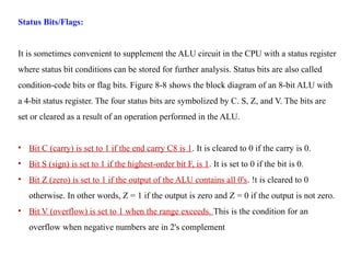
Status Bits/Flags:
It issometimes convenient to supplement the ALU circuit in the CPU with a status register
where status bit conditions can be stored for further analysis. Status bits are also called
condition-code bits or flag bits. Figure 8-8 shows the block diagram of an 8-bit ALU with
a 4-bit status register. The four status bits are symbolized by C. S, Z, and V. The bits are
set or cleared as a result of an operation performed in the ALU.
• Bit C (carry) is set to 1 if the end carry C8 is 1. It is cleared to 0 if the carry is 0.
• Bit S (sign) is set to 1 if the highest-order bit F, is 1. It is set to 0 if the bit is 0.
• Bit Z (zero) is set to 1 if the output of the ALU contains all 0's. !t is cleared to 0
otherwise. In other words, Z = 1 if the output is zero and Z = 0 if the output is not zero.
• Bit V (overflow) is set to 1 when the range exceeds. This is the condition for an
overflow when negative numbers are in 2's complement
82.
Additional Status Bits(Available in 8086 Processor):
• Bit AC (auxiliary carry) is set to 1 if there is a carry transfer from lower nibble to upper
nibble. It is cleared to 0 if there is no carry transfer from lower nibble to upper nibble.
• Bit P (parity flag) is set to 1 there are even number of 1’s in the result. It is set to 0 if
the total number of 1’s are odd in the result. [Even Parity]
83.
Questions:
Find the statusof overflow flag, carry flag, auxiliary carry flag, sign flag, zero
flag, and parity flag in following operation.
(CACA)HEX +(BABA)HEX
(CACA)HEX -(BABA)HEX
84.
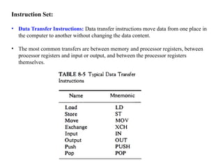
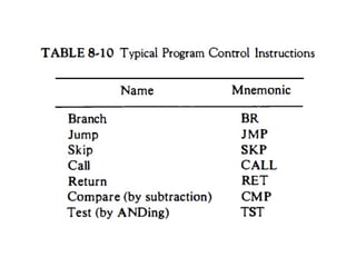
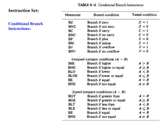
Instruction Set:
• DataTransfer Instructions: Data transfer instructions move data from one place in
the computer to another without changing the data content.
• The most common transfers are between memory and processor registers, between
processor registers and input or output, and between the processor registers
themselves.
85.
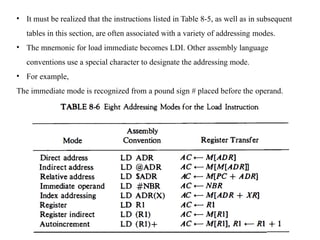
• It mustbe realized that the instructions listed in Table 8-5, as well as in subsequent
tables in this section, are often associated with a variety of addressing modes.
• The mnemonic for load immediate becomes LDI. Other assembly language
conventions use a special character to designate the addressing mode.
• For example,
The immediate mode is recognized from a pound sign # placed before the operand.
86.
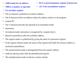
• ADR standsfor an address,
• NBR is a number or operand
• X is an index register
• The @ character symbolizes an indirect address.
• The $ character before an address makes the address relative to the program
• counter PC .
• The # character precedes the operand in an immediate-mode
• instruction.
• An indexed mode instruction is recognized by a register that is
• placed in parentheses after the symbolic address.
• The register mode is symbolized by giving the name of a processor register.
• In the register indirect mode, the name of the register that holds the memory address is
enclosed in parentheses.
• The autoincrement mode is distinguished from the register indirect
• mode by placing a plus after the parenthesized register.
• The autodecrement mode would use a minus instead.
• R1 is a general-purpose register of processor
• AC is the accumulator register.
87.
Instruction Set:
Data ManipulationInstructions:
Data manipulation instructions perform operations on data and provide the
computational capabilities for the computer.
The data manipulation instructions in a typical computer are usually divided into three
basic types:
1. Arithmetic instructions
2. Logical and bit manipulation instructions
3. Shift instructions
89.
Instruction Set:
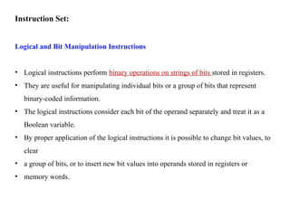
Logical andBit Manipulation Instructions
• Logical instructions perform binary operations on strings of bits stored in registers.
• They are useful for manipulating individual bits or a group of bits that represent
binary-coded information.
• The logical instructions consider each bit of the operand separately and treat it as a
Boolean variable.
• By proper application of the logical instructions it is possible to change bit values, to
clear
• a group of bits, or to insert new bit values into operands stored in registers or
• memory words.
91.
Instruction Set:
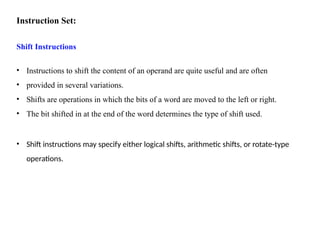
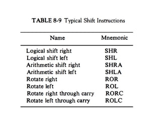
Shift Instructions
•Instructions to shift the content of an operand are quite useful and are often
• provided in several variations.
• Shifts are operations in which the bits of a word are moved to the left or right.
• The bit shifted in at the end of the word determines the type of shift used.
• Shift instructions may specify either logical shifts, arithmetic shifts, or rotate-type
operations.
93.
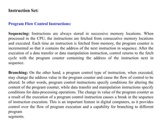
Instruction Set:
Program FlowControl Instructions:
Sequencing: Instructions are always stored in successive memory locations. When
processed in the CPU, the instructions are fetched from consecutive memory locations
and executed. Each time an instruction is fetched from memory, the program counter is
incremented so that it contains the address of the next instruction in sequence. After the
execution of a data transfer or data manipulation instruction, control returns to the fetch
cycle with the program counter containing the address of the instruction next in
sequence.
Branching: On the other hand, a program control type of instruction, when executed,
may change the address value in the program counter and cause the flow of control to be
altered. In other words, program control instructions specify conditions for altering the
content of the program counter, while data transfer and manipulation instructions specify
conditions for data-processing operations. The change in value of the program counter as
a result of the execution of a program control instruction causes a break in the sequence
of instruction execution. This is an important feature in digital computers, as it provides
control over the flow of program execution and a capability for branching to different
program
segments.
95.
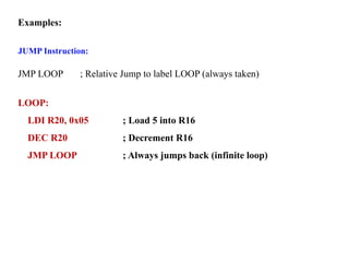
Examples:
JUMP Instruction:
JMP LOOP; Relative Jump to label LOOP (always taken)
LOOP:
LDI R20, 0x05 ; Load 5 into R16
DEC R20 ; Decrement R16
JMP LOOP ; Always jumps back (infinite loop)
96.
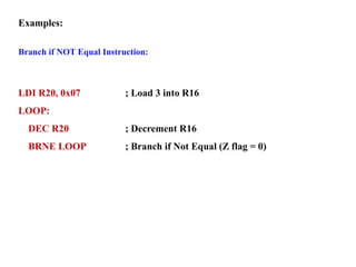
Examples:
Branch if NOTEqual Instruction:
LDI R20, 0x07 ; Load 3 into R16
LOOP:
DEC R20 ; Decrement R16
BRNE LOOP ; Branch if Not Equal (Z flag = 0)
97.
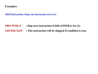
Examples:
SKIP Instruction: Skipsone instruction next to it
SBIS PINB, 0 ; Skip next instruction if bit0 of PINB is Set (1)
LDI R20, 0xFF ; This instruction will be skipped if condition is true
98.
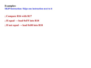
Examples:
SKIP Instruction: Skipsone instruction next to it
; Compare R16 with R17
; If equal → load 0xFF into R18
; If not equal → load 0x00 into R18
99.
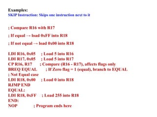
Examples:
SKIP Instruction: Skipsone instruction next to it
; Compare R16 with R17
; If equal → load 0xFF into R18
; If not equal → load 0x00 into R18
LDI R16, 0x05 ; Load 5 into R16
LDI R17, 0x05 ; Load 5 into R17
CP R16, R17 ; Compare (R16 - R17), affects flags only
BREQ EQUAL ; If Zero flag = 1 (equal), branch to EQUAL
; Not Equal case
LDI R18, 0x00 ; Load 0 into R18
RJMP END
EQUAL:
LDI R18, 0xFF ; Load 255 into R18
END:
NOP ; Program ends here
Instruction Set:
Write aprogram to find whether A=B, A>B, or A<B.
Write a program for addition of two 16-bit data in an 8-bit processor.
102.
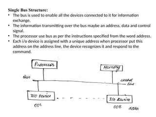
Single Bus Structure:
•The bus is used to enable all the devices connected to it for information
exchange.
• The information transmitting over the bus maybe an address, data and control
signal.
• The processor use bus as per the instructions specified from the word address.
• Each i/o device is assigned with a unique address when processor put this
address on the address line, the device recognizes it and respond to the
command.
103.
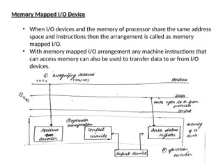
Memory Mapped I/ODevice
• When I/O devices and the memory of processor share the same address
space and instructions then the arrangement is called as memory
mapped I/O.
• With memory mapped I/O arrangement any machine instructions that
can access memory can also be used to transfer data to or from I/O
devices.
104.
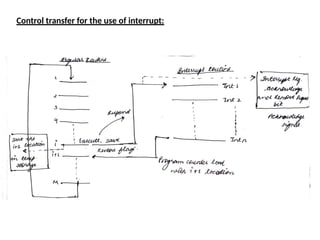
Interrupts:
• Interrupt canbe termed as an interfere request given to the
processor to interrupt its ongoing process of execution (if allowed)
so that processor can process all the processing in a timely manner.
• When the interrupt request is accepted by the processor, then the
processor will suspend its current activity, save its state and
execute a function called as interrupt handler or interrupt service
routine.
• Mainly this interruption is often temporarily, allowing the
processor to resume on its routine activity post finishing the
interrupt handling function.
• The main function of the interrupt is to indicate any special
electronic or physical state change that requires sensitive attention
by the processor.
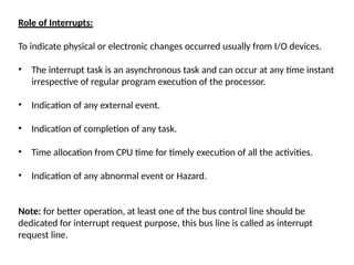
Role of Interrupts:
Toindicate physical or electronic changes occurred usually from I/O devices.
• The interrupt task is an asynchronous task and can occur at any time instant
irrespective of regular program execution of the processor.
• Indication of any external event.
• Indication of completion of any task.
• Time allocation from CPU time for timely execution of all the activities.
• Indication of any abnormal event or Hazard.
Note: for better operation, at least one of the bus control line should be
dedicated for interrupt request purpose, this bus line is called as interrupt
request line.
107.
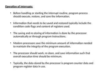
Operation of Interrupts:
•Before handling or starting the interrupt routine, program process
should execute, restore, and save the information.
• Information that needs to be saved and restored typically include the
condition code flags and content of registers used.
• The saving and re-storing of information is done by the processor
automatically or through program instructions.
• Modern processors save the minimum amount of information needed
to maintain the integrity of the program execution.
• The processor should work, re-store, and save information such that
overall execution time should be minimum.
• Typically, the data stored by the processor is program counter data and
program register data in use.
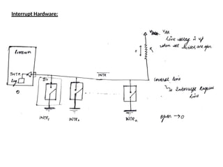
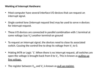
Working of InterruptHardware:
• Most computer have several interface I/O devices that can request an
interrupt signal.
• Single control lone (interrupt request line) may be used to serve n devices
for interrupt request.
• These I/O devices are connected in parallel combination with 1 terminal at
same voltage (say V1) another terminal on ground
• To request an interrupt signal, the devices need to close its associated
switch. Causing the control line to drop its voltage from V1 to 0.
• Making INTR or Logic ‘1’. When there is no interrupt request, all switches are
open the voltage is brought back from 0 to V1. This in known as pulling up
line voltage.
• The register between Vdd and V1 is known as pull up register.
110.
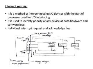
Interrupt nesting:
• Itis a method of interconnecting I/O devices with the part of
processor used for I/O interfacing.
• It is used to identify priority of any device at both hardware and
software level
• Individual interrupt request and acknowledge line
111.
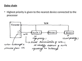
Daisy chain
• Highestpriority is given to the nearest device connected to the
processor
112.
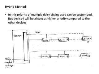
Hybrid Method
• Inthis priority of multiple daisy chains used can be customized.
But device-I will be always at higher priority compared to the
other devices
113.
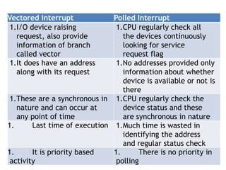
Vectored interrupt PolledInterrupt
1.I/O device raising
request, also provide
information of branch
called vector
1.CPU regularly check all
the devices continuously
looking for service
request flag
1.It does have an address
along with its request
1.No addresses provided only
information about whether
device is available or not is
there
1.These are a synchronous in
nature and can occur at
any point of time
1.CPU regularly check the
device status and these
are synchronous in nature
1. Last time of execution 1.Much time is wasted in
identifying the address
and regular status check
1. It is priority based
activity
1. There is no priority in
polling
114.
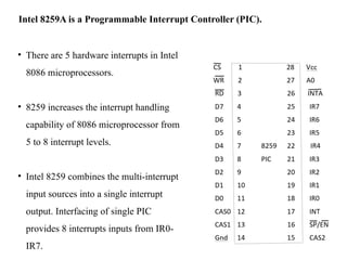
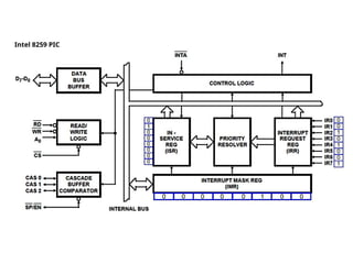
• There are5 hardware interrupts in Intel
8086 microprocessors.
• 8259 increases the interrupt handling
capability of 8086 microprocessor from
5 to 8 interrupt levels.
• Intel 8259 combines the multi-interrupt
input sources into a single interrupt
output. Interfacing of single PIC
provides 8 interrupts inputs from IR0-
IR7.
Intel 8259A is a Programmable Interrupt Controller (PIC).
115.
Features of Intel8259 PIC are as follows:
• Intel 8259 is designed for Intel 8085 and Intel 8086 microprocessor.
• Masking and unmasking of interrupts are done using IMR
• It can be programmed either in level triggered or in edge triggered interrupt
level.
• We can mask individual bits of interrupt request register.
• We can increase interrupt handling capability up to 64 interrupt level by
cascading further 8259 PICs.
116.
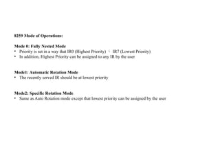
8259 Mode ofOperations:
Mode 0: Fully Nested Mode
• Priority is set in a way that IR0 (Highest Priority) IR7 (Lowest Priority)
• In addition, Highest Priority can be assigned to any IR by the user
Mode1: Automatic Rotation Mode
• The recently served IR should be at lowest priority
Mode2: Specific Rotation Mode
• Same as Auto Rotation mode except that lowest priority can be assigned by the user
Interrupt Operation:
Step1: Initializethe 8259 PIC
Step2: IRR store the current interrupt requests
Step3: Three registers are used for resolving the priority (IRR, ISR, and
IMR)
Step4: Once the interrupt is received the Interrupt will be acknowledged
through microprocessor by INTA’
Step5: Corresponding bit is set in ISR and Reset in IRR
Step6: The 8259A , places the opcode corresponds to ALL instruction on
the data bus
Which interrupt request received?
Which is currently handled interrupt?
Which interrupts are masked?
119.
Interrupt Operation:
Step7: Microprocessordecodes the CALL instruction, 8086 sends two
more INTA’ cycles
Step8: The 8259A places lower order 8-bits of interrupt branch address
on data bus during second INTA’ cycle
Step9: During the third INTA’ cycle the 8259A places the higher order 8-
bits of interrupt branch address data bus
Step10: The program sequence transfers to the memory location called
by the CALL Instruction
120.
• ICW Registers:These registers store the ICWs that are used for
initializing the PIC and setting up its initial operating
parameters.
• OCW Registers: These registers store the OCWs, which are used
to manage the operation of the PIC after it has been initialized.
This includes commands for masking/unmasking interrupts,
sending End of Interrupt (EOI) signals, rotating priorities, and
setting modes.
Control Word Register
![Dr. Mahesh Kumar (Assistant Professor, ICT)
COMPUTER DESIGN AND APPLICATION
[20ECE302T]
Week 1 – Week 3](https://image.slidesharecdn.com/cdaweek1-week5-250916182509-88b4fde2/85/Computer-Design-and-applications-basiics-1-320.jpg)
![Dr. Mahesh Kumar (Assistant Professor, ICT)
COMPUTER DESIGN AND APPLICATION
[20ECE302T]
Week 1 – Week 3](https://image.slidesharecdn.com/cdaweek1-week5-250916182509-88b4fde2/75/Computer-Design-and-applications-basiics-1-2048.jpg)

![Data Representation in Computer Systems: Signed Integer Representation
Mod 16 system for 2’s-
complement numbers
Signed numbers
• Total number for presentations are 2n
(Here n is number of bits for
representation)
• This representation contains half
positive numbers and half negative
numbers
• Range is specified in two categories
• Positive Range [0 (2n
/2 - 1)]
• Negative Range [- 2n
/2 - 1]](https://image.slidesharecdn.com/cdaweek1-week5-250916182509-88b4fde2/85/Computer-Design-and-applications-basiics-16-320.jpg)

![Memory Locations and Addresses
Question: Consider a data which needs to be stored in the byte addressability
format for a memory with word length of 32-bit.
0X1A2B3C4D5E6F0784
Represent the given number in byte addressability with both big end and little end
method.
Answer:
A 32-bit word length memory will be able to manage 4 bytes of data in a single
word
The current data needs to be stored in the memory is in hexadecimal
representation
hence the bytes will be [1A], [2B], [3C], [4D], [5E], [6F], [07], [84]](https://image.slidesharecdn.com/cdaweek1-week5-250916182509-88b4fde2/85/Computer-Design-and-applications-basiics-23-320.jpg)
![Memory Locations and Addresses
Big-End method Byte addressability
Representation will be as follows
In byte addressability 8-bit data go together
In Hexadecimal:
Word 1: [1A] [2B] [3C] [4D]
Word 2: [5E] [6F] [07] [84]
In Binary:
Word 1: [0001 1010] [0010 1011] [0011 1100] [0100
1101]
Word 2: [0101 1110] [0110 1111] [0000 0111] [1000
0100]](https://image.slidesharecdn.com/cdaweek1-week5-250916182509-88b4fde2/85/Computer-Design-and-applications-basiics-24-320.jpg)
![Memory Locations and Addresses
Little-End method Byte addressability
Representation will be as follows
In byte addressability 8-bit data go together
In Hexadecimal:
Word 1: [4D] [3C] [2B] [1A]
Word 2: [84] [07] [6F] [5E]
In Binary:
Word 1: [0100 1101] [0011 1100] [0010 1011] [0001
1010]
Word 2: [1000 0100] [0000 0111] [0110 1111] [0101
1110]](https://image.slidesharecdn.com/cdaweek1-week5-250916182509-88b4fde2/85/Computer-Design-and-applications-basiics-25-320.jpg)
![Register Transfer Language/Notations:
• Used to describe the transfer of information from one location to another.
• Possible transfers are memory locations, processor registers, or registers in the
I/O subsystem
• It has some sources and destination
a. Memory to Register Transfer
In this the data is transferred from some place in memory/location/local variable to
a processor register. The notation is described
R2 ← [LOC]
b. Register to Register Transfer
R4 ← [R2] + [R3]
c. Memory to I/O Device
R4 ← [Input Device]
[OUT STATUS] ← R4](https://image.slidesharecdn.com/cdaweek1-week5-250916182509-88b4fde2/85/Computer-Design-and-applications-basiics-27-320.jpg)
![Bus and Memory Transfer
Memory Transfer:
The transfer of information from a memory word to the outside environment is
called a read operation.
The transfer of new information to be stored into the memory is called a write
operation.
Memory Read: DR ← M[AR]
Memory Write: R3 ← R1 + R2’ + 1
Here
DR – Data Register
AR – Address Register
M – Memory](https://image.slidesharecdn.com/cdaweek1-week5-250916182509-88b4fde2/85/Computer-Design-and-applications-basiics-34-320.jpg)
![Instruction Formats
Three-Address Instructions
Evaluate X = (A + B) * (C + D) using Three-Address instructions
ADD R1, A, B // R1 ← M[A] + M[B]
ADD R2, C, D // R2 ← M[C] + M[D]
MUL X, R1, R2 // M[X] ← R1 * R2](https://image.slidesharecdn.com/cdaweek1-week5-250916182509-88b4fde2/85/Computer-Design-and-applications-basiics-60-320.jpg)
![Instruction Formats
Two-Address Instructions
Evaluate X = (A + B) * (C + D) using Two-Address instructions
MOV R1, A // R1 ← M[A]
ADD R1, B // R1 ← R1 + M[B]
MOV R2, C // R2 ← M[C]
ADD R2, D // R2 ← R2 + M[D]
MUL R1, R2 // R1 ← R1 * R2
MOV X, R1 // M[X] ← R1](https://image.slidesharecdn.com/cdaweek1-week5-250916182509-88b4fde2/85/Computer-Design-and-applications-basiics-61-320.jpg)
![Instruction Formats
One-Address Instructions
Use an implied AC register for all data manipulation
Evaluate X = (A + B) * (C + D) using One-Address instructions
LOAD A AC ← M[A]
ADD B AC ← AC + M[B]
STORE T M[T] ← AC
LOAD C AC ← M[C]
ADD D AC ← AC + M[D]
MUL T AC ← AC * M[T]
STORE X M[X] ← AC
Here AC is accumulator](https://image.slidesharecdn.com/cdaweek1-week5-250916182509-88b4fde2/85/Computer-Design-and-applications-basiics-62-320.jpg)
![Instruction Formats
Zero-Address Instructions
Evaluate X = (A + B) * (C + D) using One-Address instructions
PUSH A TOS ← A
PUSH B TOS ← B
ADD TOS ← (A + B)
PUSH C TOS ← C
PUSH D TOS ← D
ADD TOS ← (C + D)
MUL TOS ← (C + D) * (A + B)
POP X M[X] ← TOS
TOS – Top of Stack](https://image.slidesharecdn.com/cdaweek1-week5-250916182509-88b4fde2/85/Computer-Design-and-applications-basiics-63-320.jpg)

![Questions on reverse polish notation for writing program in zero address format.
Give Zero, one, two and three address programs for given equations:
Q1: A * B + C * D + E * F
Ans: AB*CD*EF*+ +
Q2: A * B + A * (B * D + C * E)
Ans: AB*ABD*CE*+*+
Q3: [ A * [ B + C * ( D + E ) ] ] / [ F * ( G + H ) ]
Ans: ABCDE+*+*FGH+*/](https://image.slidesharecdn.com/cdaweek1-week5-250916182509-88b4fde2/85/Computer-Design-and-applications-basiics-65-320.jpg)
![Find the Reverse Polish Notation:
Do the following question by yourself
Q4. (A + B * C) / (D – E * F + G * H)
Q5. A + B * [C * D + E * (F + G)]
Q6. (A + B – C) / (D * (5 * F – G))
Q7. (A – B + C * (D * E – F)) / (G + H * K)](https://image.slidesharecdn.com/cdaweek1-week5-250916182509-88b4fde2/85/Computer-Design-and-applications-basiics-66-320.jpg)
![Various Indirect Modes of Operand Access
Index mode—The effective address of the operand is generated by adding a
constant value to the contents of a register.
X(Ri)
EA = X + [Ri]](https://image.slidesharecdn.com/cdaweek1-week5-250916182509-88b4fde2/85/Computer-Design-and-applications-basiics-77-320.jpg)
![Various Indirect Modes of Operand Access
Index mode—The effective address of the operand is generated by adding a
constant value to the contents of a register.
X(Ri)
EA = X + [Ri]](https://image.slidesharecdn.com/cdaweek1-week5-250916182509-88b4fde2/85/Computer-Design-and-applications-basiics-78-320.jpg)
![Additional Status Bits (Available in 8086 Processor):
• Bit AC (auxiliary carry) is set to 1 if there is a carry transfer from lower nibble to upper
nibble. It is cleared to 0 if there is no carry transfer from lower nibble to upper nibble.
• Bit P (parity flag) is set to 1 there are even number of 1’s in the result. It is set to 0 if
the total number of 1’s are odd in the result. [Even Parity]](https://image.slidesharecdn.com/cdaweek1-week5-250916182509-88b4fde2/85/Computer-Design-and-applications-basiics-82-320.jpg)

![Unit-1_Digital Computers, number systemCOA[1].pptx](https://cdn.slidesharecdn.com/ss_thumbnails/unit-1coa1-240405124150-33a3b730-thumbnail.jpg?width=640&height=640&fit=bounds)