тізбек бөлігі үшін ом заңы
•Download as DOC, PDF•
0 likes•9,654 views

тізбек бөлігі үшін ом заңы

Recommended
More Related Content
What's hot
What's hot (19)
Viewers also liked
Viewers also liked (13)
Similar to тізбек бөлігі үшін ом заңы
Similar to тізбек бөлігі үшін ом заңы (14)
More from Айбек Қуандықұлы
More from Айбек Қуандықұлы (20)
тізбек бөлігі үшін ом заңы
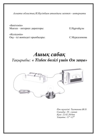
- 1. Алматы облыстық И.Нүсіпбаев атындағы мектеп - интернаты «Бекітемін» Мектеп – интернат директоры: Е.Нұртайұлы «Келісемін» Оқу - ісі жөніндегі орынбасары: С.Мурсалимова Ашық сабақ Тақырыбы: « Тізбек бөлігі үшін Ом заңы» Пән мұғалімі: Тастанова Ж.О. Сыныбы: 10 - сынып Күні: 22.02.2016ж Уақыты: 1155 -1240
- 2. Алматы қаласы, 2016 ж. Сабақтың тақырыбы: §9.3 Тізбек бөлігі үшін Ом заңы Сабақтың білімділік мақсаты: Электр тізбегіндегі кернеу мен кедергінің және ток күштерінің тәуелділігін анықтау. Дамытушылық мақсаты: Эксперимент пен теорияның сәйкестігіне көз жеткізу. Ой - өрісін, қиялдарын, еркін сөйлеуін дамытып, формулаларды түрлендіре білуге үйрету Тәрбиелік мақсаты: Оқушылардың формуланы есте сақтауына және пәнге деген қызығушылын арттыруға тәрбиелеу. Сабақтың көрнекілігі: Слайдтар, деңгейлік тапсырмалар, интерактивтік тақта Құрал-жабдықтар: Амперметр, вольтметр, ток көзі В-24, кілт, резисторлар, қосқыш сымдар, Омның суреті Сабақ жоспары. І. Ұйымдастыру бөлімі ІІ. Миға шабуыл (қызығушылығын ояту) ІІІ. Мағынаны ажырату. Жаңа сабақ. ІV. Есеп шығару V. Үй тапсырмасы. VІ. Қорытынды. Оқушыларды бағалау Сабақтың барысы: 1. Ұйымдастыру бөлімі. 2. «Қызығушылығын ояту» Оқушыларға үй тапсырмасын қайталау үшін "дұрыс - бұрыс" әдісімен сұрақтарын қойылады. Ток тығыздығы дегеніміз - өткізгіштің бірлік қимасынан қандай ток өтетінін көрсететін физикалық шама. -( дұрыс). Ток күшін өлшейтін құрал волтьметр. - (бұрыс, амперметр) Электр зарядының кез келген реттелген қозғалысы - электр тогы деп аталады. (дұрыс) Ток тығыздығының өлшем бірлігі Ньютон. (бұрыс, А/м2 ) Ток күшін өлшейтін құрал амперметр өткізгішке параллель жалғанады. (бұрыс, тізбектей жалғанады) ЭҚК - нің формуласы q/t - қа тең. (бұрыс, А/ q) Кернеуді өлшейтін құрал - вольтметр. (дұрыс) Вольтметр өткізгішке тізбектей жалғанады. (бұрыс, параллель жалғанады)
- 3. ІІ. Қызығушылығын арттыру. Миға шабуыл 1. Электр тізбегін сипаттайтын шамаларды атаңдар? ( Ток күші, кернеу, кедергі) 2. Енді осы шамаларға қысқаша тоқталайық ( 1. Шаманың белгіленуі, 2. сипаттамасы, 3. өлшем бірлігі) ІІІ. Жаңа сабақ . Жаңа сабақ тақырыбы: “ Тізбек бөлігі үшін Ом заңы ”. Біз өткен сабақтарымызда ток күші мен кернеуді жеке - жеке қарастырдық. Енді бүгінгі сабағымыздың мақсаты ток күші мен кернеу және кедергілердің арасындағы өзара байланыстарды анықтап, Ом заңымен танысу. Мына суреттегі құралдарды атаңдар? 1және 2 нөміріндегі құралдарды ата, неге олай ойлайсың? ( кілт, ток көзі, резистор, амперметр, вольтметр, қосқыш сымдар. 1нөмір вольтметр, себебі ол тізбекке параллель жалғанады, ал 2 нөмір амперметр – ол тізбектей жалғанып тізбектегі ток күшін анықтайды.) Өткізгіштегі кедергі өзгермесе, онда ток күші кернеуге қалай тәуелді болады? R – const. I ~ U тура пророрционал Осы эксперимент арқылы қандай график алуға болады? Бұл графикті: Вольт- Амперлік сипаттама деп атайды I, А U, Вт
- 4. Енді біз ток күшінің кедергіге қалай тәуелді екенін қарастырайық. Реостат арқылы тізбектегі ток күшінің өзгеруін бақылайық. (Кернеуі тұрақты кезде. Ток күші артқан сайын кедергі азаяды.) Бұл график ток күші кедергіге кері пропорционал деп оқылады. (Егер U = const, I ~ ). Ток күшінің кернеу мен кедергіге тәуелділік заңын 1827 жылы неміс ғалымы Георг Ом ашты. Осы екі қорытындыдан формула құрастырайық: Бұл формуланы Тізбек бөлігі үшін Ом заңы деп атайды. Ом заңының тұжырымдамасы: “ Тізбектің бөлігіндегі ток күші – осы бөліктің ұштарындағы кернеуге тура пропорционал, өткізгіштің кедергісіне кері пропорционал болады”. Жалпы, Кедергі дегеніміз - берілген өткізгіштің өз бойымен өтетін токқа жасайтын кедергісін көрсететін физикалық шаманы айтады. s l R ρ= Кедергі бірлігі: R= 1В/1А= 1 Ом Кедергіні өлшейтін құрал: резистор( кедергі) , реостат Ом заңын қолданып есеп шығарған кезде белгісіз шаманы қалай анықтаймыз.
- 5. U=I*R R=U/I ІV. Бекіту Есеп шығару Суретте А және В өткізгіштеріндегі ток күшінің кернеуге тәуелділік графигі берілген.График бойынша қай өткізгіштің кедергісі үлкен? Неге олай ойлайсың? Себебі: Ом заңы бойынша ток күші кедергіге кері пропорционал. Кернеуі екі өткізгіште 6В, ал ток күші В өткізгіште 1А, А өткізгіште 3А ге тең. Осы айтылғанды есеп шығару арқылы дәлелдейік. Тақтаға 2оқушы шығады. Қазір біз бүгін сабақтың қорытындысын шығарайық. Ток күші, кернеу, кедергінің арасында қандай байланыс бар? (Ом заңы бойыша ток күші кернеуге тура, ал кедергіге кері пропорционал болады.)
- 6. Формула бойынша Ом заңы қалай оқылады? ( I = . Ом заңы) V. Үй тапсырмасы: Үйге тапсырма: § 9.3, Есептер жинағынан № (1,2). VІ. Қорытынды. Оқушыларды бағалау.
- 7. Формула бойынша Ом заңы қалай оқылады? ( I = . Ом заңы) V. Үй тапсырмасы: Үйге тапсырма: § 9.3, Есептер жинағынан № (1,2). VІ. Қорытынды. Оқушыларды бағалау.