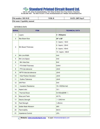
SlideShare a Scribd company logo
File number: ME-M-II                       VER: B                         DATE: 2007-Sep-9
File name: Capability manual


  GENERAL DATA

SERIAL                             ITEM                             TECHNICAL DATA

   1     Layers                                       ๏ผ
                                                     2๏ผ24(layers)

   2     Max Board Size                              24" x 28"

                                                     4๏ผˆlayers๏ผ‰16mil

                                                     6๏ผˆlayers๏ผ‰32mil
   3     Min Board Thickness
                                                     8๏ผˆlayers๏ผ‰40mil

                                                     10๏ผˆlayers๏ผ‰48mil

   4     Min Line Width                              4mil

   5     Min Line Space                              4mil

   6       Min Hole Size                             8mil

   7       PTH Wall Thickness                        0.8mil

   8       PTH dia tolerance                         ยฑ3mil

   9       NPTH hole dia tolerance                   ยฑ2mil

  10       Hole Position Deviation                   ยฑ3mil

  11       Outline Tolerance                         ยฑ4mil

  12     S/M Pitch                                   3mil

  13       Insulation Resistance                     1E+12 (Normal)

  14     Aspect ratio                                10:1

  15       Thermal Shock                             3x10Sec@288 โ„ƒ

  16     Warp and Twist                              โ‰ค0.7%

  17     Electric Strength                           ๏ผž1.3KV/mm

  18     Peel Strength                               1.4N/mm

  19     Solder Mask Abrasion                        โ‰ฅ6H

  20     Flammability                                94V-0

  21     Impedance Control                           ยฑ5%

            Website: www.standardpcb.com   E-mail: info@standardpcb.com
       1
.


                               SS/DS                        4-L                           6-L
Layers/Thickness/ Outline
Finish
Routing                        0.3~2.4                      0.5~2.4                       0.75~2.4
Punching                       0.3~1.6                      0.5~1.6                       0.75~1.6
V-cut                          0.6~2.4                      0.6~2.4                       0.75~2.4


Layers/Thickness/ Outline Finish         SS/DS                                  ML
For 0.3~0.8                              +/-0.0762                              +/-0.10
For 0.8~1.2                              +/-0.10                                +/-.127
For 1.2~                                 +/-0.127                               +/-10%


    Finish Surface: Gold Flash,    Minimum Thickness: 0.20mm
    Finish Surface: HASL,           Minimum Thickness: 0.60mm
    Finish Surface:     All,       Maximum Thickness: 3.2mm
4. Drilled Hole Size and Tolerance
    4.1 Minimum PTH Hole Size 0.15mm , Minimum PTH Slot size 0.4mm ร— 0.8mm
    4.2 Minimum NPT Hole Size 0.20mm , Minimum NPT Slot Size 0.5mm ร— 1.0mm
    4.3 Tolerance
    PTH:          +/-0.05mm(Gold flash & Entek), +0.075/-.0.05mm(HAL)min
    NPTH:         +/-0.05mm
5. Base material
    5.1 Copper Clad Laminate
                                    ร—      ร—      ร—      ร—
       5.1.1 Standard Size(inch): 42ร—48, 41ร—49, 36ร—48, 43ร—49
       5.1.2 Thickness(mm): 0.1,0.15,0.2,0.25,0.3,0.35,0.4,0.46,0.51,0.6,0.71,
                                  0.8,0.9,1.0,1.1,1.2,1.4,1.5,1.6,2.0,2.4,3.2
       5.1.3 Copper THK:       0.5OZ(18um), 1OZ(35UM), 2OZ(70UM), 3OZ(105UM)โ€ฆโ€ฆ6OZ(210UM)
       5.1.4 Laminate Type: FR4
       5.1.5 Flammability: 94V0


        Prepreg
       Type                               1080                          2116                         7628
Thickness                           2.8mil+/-0.3mil                4.6mil+/-.5mil               7.4mil+/-.5mil
Size                                 49.5โ€x300mm                    49.5โ€300mm                  49.5โ€x150mm
              Website: www.standardpcb.com             E-mail: info@standardpcb.com
         2
6.Surface Finish and Thickness
  6.1 HASL                       1~38um in hole, 2.54~25.4um on SMT
  6.2 Gold Flash Ni:              2.5~7.62um, Au: 0.05~0.25um
  6.3 Selective Gold Plating: Ni: 2.5~7.62um, Au: 0.05~0.25um
  6.4 Immersion Gold: Ni:          2.5~7.62um, Au: 0.127~1.27um
  6.5 Gold-Edge Contacts: Ni:      2.5~7.62um, Au: 0.127~1.27um
  6.6 Entek M2602 (For single side and Double sides)


7.Solder mask
   7.1Heat Cured Ink: ZSR-150 (PA-5B, NA-402)
   7.2LPI resist ink:      Green gloss (FSR-8000-9G05, R500-2G, PSR2000-G35A, PSR4000-
                                      LDSM-3000 G-7, APR-8000 G-102)
                           Green matte (LM-600 5GM)
                           White (LSM-3000NW)
                           Black (FSR-8000 (10C10))
                           Red (LSM-3000SR)
                           Blue (FSR 8b89, LSM-3000NSBL)
                           Yellow (LSM-3000NSY-6)
    7.3    UV Ink:         Green (UVS-1000)
                           White (UVM-1800W)


8. Legend Ink
    8.1    White: (ZM-400WF)
    8.2    Black: (BK-3)
    8.3    Yellow: (ZM-400YR)
9.Carbon Ink: PR-406, TU-15ST (25 Ohm/square)


10.Peelable Mask: B99-84B, PETERS SD 2955


            Website: www.standardpcb.com         E-mail: info@standardpcb.com
       3
File number: P ME-M-II                           VER: B                          DATE: 2007-Sep-9
File name: Capability manual
  5.2 Surface copper plating thickness:
                         Board type             Bonding            Flash gold          HAL & Entek
                         Copper thickness       5um~10um           10um~25um           20um~40um


6. Etching
  6.1 Etching factor: 1.5 max, 1.0Std.
  6.2 Etch tolerance:


         Board type        Flash gold                                           HAL
Line width tolerance       +/-12%                     +/-20%(L>5mil)             +/-1mil(L<=5mil)
(min.)


7. Solder Mask (LPI) Printing:
  7.1 Registration Tolerance of Solder Mask to pattern: +/-2mil (min), +/-3mils(Std)
  7.2 Solder Mask Thickness: 10um~40um on line surface, 6um min. at line edge
  7.4 Plugged Hole Size: 0.6mm (Max.)
  7.5 Minimum Solder Mask hide: 0.35mm
  7.6 Minimum Spacing of Solder Mask Opening to Line: 3mil
  7.7 Minimum solder bridge: 4mil
8. Silkscreen Printing
  8.1 Legend Printing
      8.1.1 Minimum Line Width 6mil, Minimum height of Legend 40mil
      8.1.2 Registration of Legend to Reference Hole +/-6mil
  8.2 Carbon Printing
      8.2.1 Minimum Line Width/ Spacing 10mil/14mil
      8.2.2 Registration of Carbon to Reference Hole +/-7mil
  8.3 Peelable Mask
      8.3.1 Thickness of Mask 0.2mm~0.4mm
      8.3.2 Maximum Size of Tenting hole 4.0mm
9. Profile finish:
  9.1 Outline Finish Tolerance: +/-0.1mm(min), +/-0.13mm(Std.)
  9.2 Routing
      9.2.1 Minimum Milling Cutter Size 0.8mm
      9.2.2 Minimum Radius of Inner Copper 0.4mm
             Website: www.standardpcb.com        E-mail: info@standardpcb.com
         4
9.2.3 Minimum Position Tolerance of Routing Hole (Slot) or Edge to Drill hole +/-5mil
     9.2.4 Minimum Position Tolerance of Routing Hole to Routing Hole (Slot) +/-3mil
     9.2.5 Minimum Position Tolerance of Routing Hole (Slot) to Routing Edge +/-4mil
  9.3 Punching
     9.3.1 Minimum Size of Punching Hole (Slot) 1.0mm
     9.3.2 Maximum Size of Punching Board (panel) 350mm x 270mm
     9.3.3 Maximum Thickness of Punching Board 1.6mm
     9.3.4 Minimum Position Tolerance of Punching Hole (Slot) or Edge to Drill hole +/-5mil
     9.3.5 Minimum Position Tolerance of Punching Hole to Punching Hole (Slot) +/-3mil
     9.3.6 Minimum Position Tolerance of Punching Hole (Slot) to Punching Edge +/-4mil
9.4 V-cutting
     9.4.1 Minimum Size of V-cut Board 50mm x 85 (v-cut direction) mm
     9.4.2 Minimum Thickness of V-cut Board 0.6mm
     9.4.3 Minimum Space of V-cut Line Per customer requirement
     9.4.4 Minimum Space of V-cut Line to Panel Edge 3mm
     9.4.5 Minimum Position Tolerance of V-cut Line to Primary Drilling Hole +/-7mil
     9.4.6 Minimum Position Tolerance of V-cut Line to Second Drilling Hole +/-9mil
     9.4.7 Minimum Position Tolerance of V-cut Line to Routing Edge +/-6mil
     9.4.8 Minimum Position Tolerance of V-cut Line to Punching Edge +/-7mil
     9.4.9 Minimum Position Tolerance of V-cut Line to V-cut line+/-4mil
     9.4.10 Registration Tolerance of V-cut lines +/-4mil
     9.4.11 V-Cut residual +/-4mil


10. E-Testing
     10.1 Test Voltage 50V~300V                             Commonly: 200V~300V
     10.2 Isolated Resistance 1K ohm~100M ohm               Commonly: 20M ohm~40M ohm
     10.3 Continuity Resistance 10 ohm~20K ohm              Commonly: 50 ohm~100 ohm
11. FQC
  11.1 Warp & Trap


Board Thk.           <0.5mm                0.5~0.8mm              1.0~1.2mm           >1.5mm
Warpage              1.5% max.             1% max.                0.75% max.          0.5% max.


           Website: www.standardpcb.com          E-mail: info@standardpcb.com
       5
File number: ME-M-II                 VER: B                              DATE: 2007-Spe-9
File name: Capability manual


Capability of Individual PROCESS
1. Drill Process
   Min. drill bit: 0.2mm, Max drill bit 6.5mm
   Min. working panel size: 6โ€x6โ€, Max. working panel size: 24โ€x20โ€
   Hole Position tolerance: +/-3mil (primary drilled), +/-5mil(Secondary drilled)
   Min slot drill bit: 0.5mm


2. PTH and Panel Plating
   Max. aspect ratio: 6 : 1
   Copper plating thickness 5~10um


3. Imaging (Outer)
   3.1 Minimum Line Width/Spacing 4mil/4mil (0.5OZ), 6mil/6mil (1OZ)
   3.2 Minimum SMT Pitch 16 mil, Std. SMT Pith 20mil
   3.3 Minimum Bonding Pitch 9 mil Std. Bonding Pitch 12mil
   3.4 Minimum Theoretic Annual Ring 5mil, Std. Annual Ring              6mil
   3.5 Minimum Mesh Gap: 8mil
   3.6 Maximum Size of D/F Tending Hole D5.5mm, Slot Width 4.5mm (Board Thk. 0.8mm)
   3.7 Registration tolerance of pattern to reference Hole: +/-2mil(min), +/-3mil(std.)
3.8 Film Compensation Value of Pattern:
Item                           0.5 OZ          1.0 OZ             2 OZ
Outer (expect F/G board)       0.04mm          0.08mm             0.12mm
Inner                          0.02mm          0.04mm             0.08mm


3.9 Minimum Spacing:
Item               Line-Line Line-Logo Line-Plane Copper or Line-Npth                     Pad or
                                                                                          Line-Edge(R)
Spacing            4mil       5mil      4mil        8mil                                  10mil

            Website: www.standardpcb.com          E-mail: info@standardpcb.com
        6
Item             Via Pad-Via Pad           Comp. Pad-Comp. Pad Pad or Line-Edge (V) Pad or Line-Edge
                                                                                             (P)
Spacing          4mil                      4mil or 10 mil            14 mil                  12 mil
Item             Line-Via Pad              Line-Comp. Plane          Via Pad-Plane           Comp. Pad-Plane
Spacing          4mil                      6mil                      4mil                    6mil


3.10 Imaging (Inner)
  4.1 Minimum Line Width/Spacing 4mil/4mil (0.5OZ), 6mil/6mil (1OZ)
  4.2 Minimum Theoretic Annual Ring of Signal Pad & Thermal Pad 6mil
  4.3 Minimum Theoretic Annual Ring of Non-Functional Pad 10mil
  4.4 Minimum Clearance of Isolation Pad 12mil (via) or 10mil (PTH>1mm)
  4.5 Film Compensation Value of Pattern (Ref to 3.5)
  4.6 Registration Tolerance of Layer of Layer to Layer: +/-3mil (min.), +/-4mil (Std)
  4.7 Minimum Spacing
    Item         Line-Line Line-d          Copper or Line-Npth                     Pad or Line-Edge(R)
    Spacing      4mil        4mil          8mil                                    10mil
    Item         Pad-Pad     Line-Plane    Pad or Line-Edge (V)                    Pad or Line-Edge (P)
    Spacing      5mil        4mil          14 mil                                  16 mil
    Item         Pad-Plane Plane-Plane Line-PHT Edge (isolated)
    Spacing      4mil        6mil          6mil (4L) or 8mil (>6L)


5. Pattern Plating
  5.1 Hole wall copper plating thickness
Board type                 Bonding                      Flash gold                  HAL & Entek
Copper thickness           5um~10um                     10um~20um                   18um~35um


             Website: www.standardpcb.com           E-mail: info@standardpcb.com
       7

More Related Content

What's hot

TDS F FSK750.pdf
TDS F FSK750.pdfTDS F FSK750.pdf
TDS F FSK750.pdfDENNY CHAW
ย 
Acculine xc series round cylinders of large bores
Acculine xc series round cylinders of large boresAcculine xc series round cylinders of large bores
Acculine xc series round cylinders of large bores
Acculine Precision Manufacturing Company
ย 
Borosilicate3.3
Borosilicate3.3Borosilicate3.3
Borosilicate3.3Evan Fan
ย 
ะะฑั€ะฐะทะธะฒะฝั‹ะต ะผะฐั‚ะตั€ะธะฐะปั‹ ะดะปั ะผะตั‚ะฐะปะปะพะพะฑั€ะฐะฑะฐั‚ั‹ะฒะฐัŽั‰ะตะน ะฟั€ะพะผั‹ัˆะปะตะฝะฝะพัั‚ะธ
ะะฑั€ะฐะทะธะฒะฝั‹ะต ะผะฐั‚ะตั€ะธะฐะปั‹ ะดะปั ะผะตั‚ะฐะปะปะพะพะฑั€ะฐะฑะฐั‚ั‹ะฒะฐัŽั‰ะตะน  ะฟั€ะพะผั‹ัˆะปะตะฝะฝะพัั‚ะธะะฑั€ะฐะทะธะฒะฝั‹ะต ะผะฐั‚ะตั€ะธะฐะปั‹ ะดะปั ะผะตั‚ะฐะปะปะพะพะฑั€ะฐะฑะฐั‚ั‹ะฒะฐัŽั‰ะตะน  ะฟั€ะพะผั‹ัˆะปะตะฝะฝะพัั‚ะธ
ะะฑั€ะฐะทะธะฒะฝั‹ะต ะผะฐั‚ะตั€ะธะฐะปั‹ ะดะปั ะผะตั‚ะฐะปะปะพะพะฑั€ะฐะฑะฐั‚ั‹ะฒะฐัŽั‰ะตะน ะฟั€ะพะผั‹ัˆะปะตะฝะฝะพัั‚ะธ
dedvandal
ย 
TDS F FK760.pdf
TDS F FK760.pdfTDS F FK760.pdf
TDS F FK760.pdfDENNY CHAW
ย 
TDS F FM731.pdf
TDS F FM731.pdfTDS F FM731.pdf
TDS F FM731.pdfDENNY CHAW
ย 
Industrial ceramic technology
Industrial ceramic technologyIndustrial ceramic technology
Industrial ceramic technologyINCERTECH
ย 
Incerech profile
Incerech profileIncerech profile
Incerech profile
INCERTECH
ย 
TDS F FGF795.pdf
TDS F FGF795.pdfTDS F FGF795.pdf
TDS F FGF795.pdfDENNY CHAW
ย 
Pmma properties data sheet_ gevacril
Pmma  properties data sheet_ gevacrilPmma  properties data sheet_ gevacril
Pmma properties data sheet_ gevacrilmandalika3
ย 
TDS F PSK3050.pdf
TDS F PSK3050.pdfTDS F PSK3050.pdf
TDS F PSK3050.pdfDENNY CHAW
ย 
Technical data sheet of double sided foil sandwiched woven cloth facing (FWF780)
Technical data sheet of double sided foil sandwiched woven cloth facing (FWF780)Technical data sheet of double sided foil sandwiched woven cloth facing (FWF780)
Technical data sheet of double sided foil sandwiched woven cloth facing (FWF780)
DENNY CHAW
ย 
Sun Tk300 U Fiber Connector Termination Tool Kit
Sun Tk300 U Fiber Connector Termination Tool KitSun Tk300 U Fiber Connector Termination Tool Kit
Sun Tk300 U Fiber Connector Termination Tool Kit
Villat2012
ย 
Solar Flat plate collector
Solar Flat plate collectorSolar Flat plate collector
Solar Flat plate collector
Jussi Han
ย 
Pmma properties data sheet _ gehr
Pmma properties data sheet _ gehrPmma properties data sheet _ gehr
Pmma properties data sheet _ gehrmandalika3
ย 
TDS F FM1831.pdf
TDS F FM1831.pdfTDS F FM1831.pdf
TDS F FM1831.pdfDENNY CHAW
ย 
TDS F FK750.pdf
TDS F FK750.pdfTDS F FK750.pdf
TDS F FK750.pdfDENNY CHAW
ย 
USTEK Pcb Presentation
USTEK Pcb PresentationUSTEK Pcb Presentation
USTEK Pcb Presentation
USTEK
ย 
Benchmark of metal strip current sensing resistors 20101203
Benchmark of metal strip current sensing resistors 20101203Benchmark of metal strip current sensing resistors 20101203
Benchmark of metal strip current sensing resistors 20101203
imexsean
ย 
7.1.3fixedtypes
7.1.3fixedtypes7.1.3fixedtypes
7.1.3fixedtypesTalia Carbis
ย 

What's hot (20)

TDS F FSK750.pdf
TDS F FSK750.pdfTDS F FSK750.pdf
TDS F FSK750.pdf
ย 
Acculine xc series round cylinders of large bores
Acculine xc series round cylinders of large boresAcculine xc series round cylinders of large bores
Acculine xc series round cylinders of large bores
ย 
Borosilicate3.3
Borosilicate3.3Borosilicate3.3
Borosilicate3.3
ย 
ะะฑั€ะฐะทะธะฒะฝั‹ะต ะผะฐั‚ะตั€ะธะฐะปั‹ ะดะปั ะผะตั‚ะฐะปะปะพะพะฑั€ะฐะฑะฐั‚ั‹ะฒะฐัŽั‰ะตะน ะฟั€ะพะผั‹ัˆะปะตะฝะฝะพัั‚ะธ
ะะฑั€ะฐะทะธะฒะฝั‹ะต ะผะฐั‚ะตั€ะธะฐะปั‹ ะดะปั ะผะตั‚ะฐะปะปะพะพะฑั€ะฐะฑะฐั‚ั‹ะฒะฐัŽั‰ะตะน  ะฟั€ะพะผั‹ัˆะปะตะฝะฝะพัั‚ะธะะฑั€ะฐะทะธะฒะฝั‹ะต ะผะฐั‚ะตั€ะธะฐะปั‹ ะดะปั ะผะตั‚ะฐะปะปะพะพะฑั€ะฐะฑะฐั‚ั‹ะฒะฐัŽั‰ะตะน  ะฟั€ะพะผั‹ัˆะปะตะฝะฝะพัั‚ะธ
ะะฑั€ะฐะทะธะฒะฝั‹ะต ะผะฐั‚ะตั€ะธะฐะปั‹ ะดะปั ะผะตั‚ะฐะปะปะพะพะฑั€ะฐะฑะฐั‚ั‹ะฒะฐัŽั‰ะตะน ะฟั€ะพะผั‹ัˆะปะตะฝะฝะพัั‚ะธ
ย 
TDS F FK760.pdf
TDS F FK760.pdfTDS F FK760.pdf
TDS F FK760.pdf
ย 
TDS F FM731.pdf
TDS F FM731.pdfTDS F FM731.pdf
TDS F FM731.pdf
ย 
Industrial ceramic technology
Industrial ceramic technologyIndustrial ceramic technology
Industrial ceramic technology
ย 
Incerech profile
Incerech profileIncerech profile
Incerech profile
ย 
TDS F FGF795.pdf
TDS F FGF795.pdfTDS F FGF795.pdf
TDS F FGF795.pdf
ย 
Pmma properties data sheet_ gevacril
Pmma  properties data sheet_ gevacrilPmma  properties data sheet_ gevacril
Pmma properties data sheet_ gevacril
ย 
TDS F PSK3050.pdf
TDS F PSK3050.pdfTDS F PSK3050.pdf
TDS F PSK3050.pdf
ย 
Technical data sheet of double sided foil sandwiched woven cloth facing (FWF780)
Technical data sheet of double sided foil sandwiched woven cloth facing (FWF780)Technical data sheet of double sided foil sandwiched woven cloth facing (FWF780)
Technical data sheet of double sided foil sandwiched woven cloth facing (FWF780)
ย 
Sun Tk300 U Fiber Connector Termination Tool Kit
Sun Tk300 U Fiber Connector Termination Tool KitSun Tk300 U Fiber Connector Termination Tool Kit
Sun Tk300 U Fiber Connector Termination Tool Kit
ย 
Solar Flat plate collector
Solar Flat plate collectorSolar Flat plate collector
Solar Flat plate collector
ย 
Pmma properties data sheet _ gehr
Pmma properties data sheet _ gehrPmma properties data sheet _ gehr
Pmma properties data sheet _ gehr
ย 
TDS F FM1831.pdf
TDS F FM1831.pdfTDS F FM1831.pdf
TDS F FM1831.pdf
ย 
TDS F FK750.pdf
TDS F FK750.pdfTDS F FK750.pdf
TDS F FK750.pdf
ย 
USTEK Pcb Presentation
USTEK Pcb PresentationUSTEK Pcb Presentation
USTEK Pcb Presentation
ย 
Benchmark of metal strip current sensing resistors 20101203
Benchmark of metal strip current sensing resistors 20101203Benchmark of metal strip current sensing resistors 20101203
Benchmark of metal strip current sensing resistors 20101203
ย 
7.1.3fixedtypes
7.1.3fixedtypes7.1.3fixedtypes
7.1.3fixedtypes
ย 

Similar to PCB manufacturer, PCB manufacturing | Spcb capability manual

Http --www raypcb-com-rigid-pcb-capacity
Http --www raypcb-com-rigid-pcb-capacityHttp --www raypcb-com-rigid-pcb-capacity
Http --www raypcb-com-rigid-pcb-capacityraymingpcb
ย 
TGS Presentation at CART2012
TGS Presentation at CART2012TGS Presentation at CART2012
TGS Presentation at CART2012
wenhuaiwanqi
ย 
20 Ghz Crossover
20 Ghz Crossover20 Ghz Crossover
20 Ghz Crossover
MikeWalsh1954
ย 
trial Connector 14183 jst-eph
trial Connector 14183 jst-ephtrial Connector 14183 jst-eph
trial Connector 14183 jst-eph
Jose Rafael Soria
ย 
Connector 14183 jst-eph
Connector 14183 jst-ephConnector 14183 jst-eph
Connector 14183 jst-eph
Jose Rafael Soria
ย 
Rigid-flex Circuit PCB Presentation | XPCB Limited
Rigid-flex Circuit PCB Presentation | XPCB LimitedRigid-flex Circuit PCB Presentation | XPCB Limited
Rigid-flex Circuit PCB Presentation | XPCB Limited
Ivy | XPCB Ltd
ย 
Ray ming profile
Ray ming profileRay ming profile
Ray ming profile
sinnshun
ย 
Ofc2018
Ofc2018Ofc2018
Ofc2018
TakafumiCHIBA
ย 
Luckystar Company Profile-Lisa
Luckystar Company Profile-LisaLuckystar Company Profile-Lisa
Luckystar Company Profile-LisaLisa Luo
ย 
24 c armored patch cable
24 c armored patch cable24 c armored patch cable
24 c armored patch cableSun Telecom
ย 
Ac mandev broucher_25_09_2019_new_5_6_1[1] (1)
Ac mandev broucher_25_09_2019_new_5_6_1[1] (1)Ac mandev broucher_25_09_2019_new_5_6_1[1] (1)
Ac mandev broucher_25_09_2019_new_5_6_1[1] (1)
Anupam Sharma
ย 
New corporate presentation july 2010
New corporate presentation july 2010New corporate presentation july 2010
New corporate presentation july 2010
Tony Monaco
ย 
Nextpcb capabilities 170921
Nextpcb capabilities 170921Nextpcb capabilities 170921
Nextpcb capabilities 170921
NextPCB.com - Next Day Get Your PCB!
ย 
Next pcb capabilities
Next pcb capabilitiesNext pcb capabilities
Next pcb capabilities
Kwok Tsun
ย 
Our production capability for flexible pcb & rigid pcb
Our production capability for flexible pcb & rigid pcbOur production capability for flexible pcb & rigid pcb
Our production capability for flexible pcb & rigid pcb
wonderfulpcbnet
ย 
M 02.8 rev02 capitolato tecnico di fornitura technical specifications
M 02.8 rev02 capitolato tecnico di fornitura   technical specificationsM 02.8 rev02 capitolato tecnico di fornitura   technical specifications
M 02.8 rev02 capitolato tecnico di fornitura technical specifications
EnricoFioravanti2
ย 
Quest pcb
Quest pcbQuest pcb
Quest pcbSmarterSMB
ย 
Figure-8 Aerial Fiber-SUN-FIG8-24P-SM
Figure-8 Aerial Fiber-SUN-FIG8-24P-SMFigure-8 Aerial Fiber-SUN-FIG8-24P-SM
Figure-8 Aerial Fiber-SUN-FIG8-24P-SM
Sun Telecommunication (Shanghai) Co., Ltd.
ย 
Dr.R.Narayanasamy - Formability of Automobile grade steels
Dr.R.Narayanasamy - Formability of Automobile grade steelsDr.R.Narayanasamy - Formability of Automobile grade steels
Dr.R.Narayanasamy - Formability of Automobile grade steels
Dr.Ramaswamy Narayanasamy
ย 
Printed Circuits at EFPCB
Printed Circuits at EFPCBPrinted Circuits at EFPCB
Printed Circuits at EFPCB
High Quality PCB Co., Limited
ย 

Similar to PCB manufacturer, PCB manufacturing | Spcb capability manual (20)

Http --www raypcb-com-rigid-pcb-capacity
Http --www raypcb-com-rigid-pcb-capacityHttp --www raypcb-com-rigid-pcb-capacity
Http --www raypcb-com-rigid-pcb-capacity
ย 
TGS Presentation at CART2012
TGS Presentation at CART2012TGS Presentation at CART2012
TGS Presentation at CART2012
ย 
20 Ghz Crossover
20 Ghz Crossover20 Ghz Crossover
20 Ghz Crossover
ย 
trial Connector 14183 jst-eph
trial Connector 14183 jst-ephtrial Connector 14183 jst-eph
trial Connector 14183 jst-eph
ย 
Connector 14183 jst-eph
Connector 14183 jst-ephConnector 14183 jst-eph
Connector 14183 jst-eph
ย 
Rigid-flex Circuit PCB Presentation | XPCB Limited
Rigid-flex Circuit PCB Presentation | XPCB LimitedRigid-flex Circuit PCB Presentation | XPCB Limited
Rigid-flex Circuit PCB Presentation | XPCB Limited
ย 
Ray ming profile
Ray ming profileRay ming profile
Ray ming profile
ย 
Ofc2018
Ofc2018Ofc2018
Ofc2018
ย 
Luckystar Company Profile-Lisa
Luckystar Company Profile-LisaLuckystar Company Profile-Lisa
Luckystar Company Profile-Lisa
ย 
24 c armored patch cable
24 c armored patch cable24 c armored patch cable
24 c armored patch cable
ย 
Ac mandev broucher_25_09_2019_new_5_6_1[1] (1)
Ac mandev broucher_25_09_2019_new_5_6_1[1] (1)Ac mandev broucher_25_09_2019_new_5_6_1[1] (1)
Ac mandev broucher_25_09_2019_new_5_6_1[1] (1)
ย 
New corporate presentation july 2010
New corporate presentation july 2010New corporate presentation july 2010
New corporate presentation july 2010
ย 
Nextpcb capabilities 170921
Nextpcb capabilities 170921Nextpcb capabilities 170921
Nextpcb capabilities 170921
ย 
Next pcb capabilities
Next pcb capabilitiesNext pcb capabilities
Next pcb capabilities
ย 
Our production capability for flexible pcb & rigid pcb
Our production capability for flexible pcb & rigid pcbOur production capability for flexible pcb & rigid pcb
Our production capability for flexible pcb & rigid pcb
ย 
M 02.8 rev02 capitolato tecnico di fornitura technical specifications
M 02.8 rev02 capitolato tecnico di fornitura   technical specificationsM 02.8 rev02 capitolato tecnico di fornitura   technical specifications
M 02.8 rev02 capitolato tecnico di fornitura technical specifications
ย 
Quest pcb
Quest pcbQuest pcb
Quest pcb
ย 
Figure-8 Aerial Fiber-SUN-FIG8-24P-SM
Figure-8 Aerial Fiber-SUN-FIG8-24P-SMFigure-8 Aerial Fiber-SUN-FIG8-24P-SM
Figure-8 Aerial Fiber-SUN-FIG8-24P-SM
ย 
Dr.R.Narayanasamy - Formability of Automobile grade steels
Dr.R.Narayanasamy - Formability of Automobile grade steelsDr.R.Narayanasamy - Formability of Automobile grade steels
Dr.R.Narayanasamy - Formability of Automobile grade steels
ย 
Printed Circuits at EFPCB
Printed Circuits at EFPCBPrinted Circuits at EFPCB
Printed Circuits at EFPCB
ย 

Recently uploaded

Search Disrupted Googleโ€™s Leaked Documents Rock the SEO World.pdf
Search Disrupted Googleโ€™s Leaked Documents Rock the SEO World.pdfSearch Disrupted Googleโ€™s Leaked Documents Rock the SEO World.pdf
Search Disrupted Googleโ€™s Leaked Documents Rock the SEO World.pdf
Arihant Webtech Pvt. Ltd
ย 
5 Things You Need To Know Before Hiring a Videographer
5 Things You Need To Know Before Hiring a Videographer5 Things You Need To Know Before Hiring a Videographer
5 Things You Need To Know Before Hiring a Videographer
ofm712785
ย 
Pitch Deck Teardown: RAW Dating App's $3M Angel deck
Pitch Deck Teardown: RAW Dating App's $3M Angel deckPitch Deck Teardown: RAW Dating App's $3M Angel deck
Pitch Deck Teardown: RAW Dating App's $3M Angel deck
HajeJanKamps
ย 
Filing Your Delaware Franchise Tax A Detailed Guide
Filing Your Delaware Franchise Tax A Detailed GuideFiling Your Delaware Franchise Tax A Detailed Guide
Filing Your Delaware Franchise Tax A Detailed Guide
YourLegal Accounting
ย 
Lookback Analysis
Lookback AnalysisLookback Analysis
Lookback Analysis
Safe PaaS
ย 
Buy Verified PayPal Account | Buy Google 5 Star Reviews
Buy Verified PayPal Account | Buy Google 5 Star ReviewsBuy Verified PayPal Account | Buy Google 5 Star Reviews
Buy Verified PayPal Account | Buy Google 5 Star Reviews
usawebmarket
ย 
PriyoShop Celebration Pohela Falgun Mar 20, 2024
PriyoShop Celebration Pohela Falgun Mar 20, 2024PriyoShop Celebration Pohela Falgun Mar 20, 2024
PriyoShop Celebration Pohela Falgun Mar 20, 2024
PriyoShop.com LTD
ย 
The Parable of the Pipeline a book every new businessman or business student ...
The Parable of the Pipeline a book every new businessman or business student ...The Parable of the Pipeline a book every new businessman or business student ...
The Parable of the Pipeline a book every new businessman or business student ...
awaisafdar
ย 
Premium MEAN Stack Development Solutions for Modern Businesses
Premium MEAN Stack Development Solutions for Modern BusinessesPremium MEAN Stack Development Solutions for Modern Businesses
Premium MEAN Stack Development Solutions for Modern Businesses
SynapseIndia
ย 
Role of Remote Sensing and Monitoring in Mining
Role of Remote Sensing and Monitoring in MiningRole of Remote Sensing and Monitoring in Mining
Role of Remote Sensing and Monitoring in Mining
Naaraayani Minerals Pvt.Ltd
ย 
RMD24 | Retail media: hoe zet je dit in als je geen AH of Unilever bent? Heid...
RMD24 | Retail media: hoe zet je dit in als je geen AH of Unilever bent? Heid...RMD24 | Retail media: hoe zet je dit in als je geen AH of Unilever bent? Heid...
RMD24 | Retail media: hoe zet je dit in als je geen AH of Unilever bent? Heid...
BBPMedia1
ย 
Memorandum Of Association Constitution of Company.ppt
Memorandum Of Association Constitution of Company.pptMemorandum Of Association Constitution of Company.ppt
Memorandum Of Association Constitution of Company.ppt
seri bangash
ย 
Attending a job Interview for B1 and B2 Englsih learners
Attending a job Interview for B1 and B2 Englsih learnersAttending a job Interview for B1 and B2 Englsih learners
Attending a job Interview for B1 and B2 Englsih learners
Erika906060
ย 
The-McKinsey-7S-Framework. strategic management
The-McKinsey-7S-Framework. strategic managementThe-McKinsey-7S-Framework. strategic management
The-McKinsey-7S-Framework. strategic management
Bojamma2
ย 
20240425_ TJ Communications Credentials_compressed.pdf
20240425_ TJ Communications Credentials_compressed.pdf20240425_ TJ Communications Credentials_compressed.pdf
20240425_ TJ Communications Credentials_compressed.pdf
tjcomstrang
ย 
What are the main advantages of using HR recruiter services.pdf
What are the main advantages of using HR recruiter services.pdfWhat are the main advantages of using HR recruiter services.pdf
What are the main advantages of using HR recruiter services.pdf
HumanResourceDimensi1
ย 
Improving profitability for small business
Improving profitability for small businessImproving profitability for small business
Improving profitability for small business
Ben Wann
ย 
Exploring Patterns of Connection with Social Dreaming
Exploring Patterns of Connection with Social DreamingExploring Patterns of Connection with Social Dreaming
Exploring Patterns of Connection with Social Dreaming
Nicola Wreford-Howard
ย 
Affordable Stationery Printing Services in Jaipur | Navpack n Print
Affordable Stationery Printing Services in Jaipur | Navpack n PrintAffordable Stationery Printing Services in Jaipur | Navpack n Print
Affordable Stationery Printing Services in Jaipur | Navpack n Print
Navpack & Print
ย 
Accpac to QuickBooks Conversion Navigating the Transition with Online Account...
Accpac to QuickBooks Conversion Navigating the Transition with Online Account...Accpac to QuickBooks Conversion Navigating the Transition with Online Account...
Accpac to QuickBooks Conversion Navigating the Transition with Online Account...
PaulBryant58
ย 

Recently uploaded (20)

Search Disrupted Googleโ€™s Leaked Documents Rock the SEO World.pdf
Search Disrupted Googleโ€™s Leaked Documents Rock the SEO World.pdfSearch Disrupted Googleโ€™s Leaked Documents Rock the SEO World.pdf
Search Disrupted Googleโ€™s Leaked Documents Rock the SEO World.pdf
ย 
5 Things You Need To Know Before Hiring a Videographer
5 Things You Need To Know Before Hiring a Videographer5 Things You Need To Know Before Hiring a Videographer
5 Things You Need To Know Before Hiring a Videographer
ย 
Pitch Deck Teardown: RAW Dating App's $3M Angel deck
Pitch Deck Teardown: RAW Dating App's $3M Angel deckPitch Deck Teardown: RAW Dating App's $3M Angel deck
Pitch Deck Teardown: RAW Dating App's $3M Angel deck
ย 
Filing Your Delaware Franchise Tax A Detailed Guide
Filing Your Delaware Franchise Tax A Detailed GuideFiling Your Delaware Franchise Tax A Detailed Guide
Filing Your Delaware Franchise Tax A Detailed Guide
ย 
Lookback Analysis
Lookback AnalysisLookback Analysis
Lookback Analysis
ย 
Buy Verified PayPal Account | Buy Google 5 Star Reviews
Buy Verified PayPal Account | Buy Google 5 Star ReviewsBuy Verified PayPal Account | Buy Google 5 Star Reviews
Buy Verified PayPal Account | Buy Google 5 Star Reviews
ย 
PriyoShop Celebration Pohela Falgun Mar 20, 2024
PriyoShop Celebration Pohela Falgun Mar 20, 2024PriyoShop Celebration Pohela Falgun Mar 20, 2024
PriyoShop Celebration Pohela Falgun Mar 20, 2024
ย 
The Parable of the Pipeline a book every new businessman or business student ...
The Parable of the Pipeline a book every new businessman or business student ...The Parable of the Pipeline a book every new businessman or business student ...
The Parable of the Pipeline a book every new businessman or business student ...
ย 
Premium MEAN Stack Development Solutions for Modern Businesses
Premium MEAN Stack Development Solutions for Modern BusinessesPremium MEAN Stack Development Solutions for Modern Businesses
Premium MEAN Stack Development Solutions for Modern Businesses
ย 
Role of Remote Sensing and Monitoring in Mining
Role of Remote Sensing and Monitoring in MiningRole of Remote Sensing and Monitoring in Mining
Role of Remote Sensing and Monitoring in Mining
ย 
RMD24 | Retail media: hoe zet je dit in als je geen AH of Unilever bent? Heid...
RMD24 | Retail media: hoe zet je dit in als je geen AH of Unilever bent? Heid...RMD24 | Retail media: hoe zet je dit in als je geen AH of Unilever bent? Heid...
RMD24 | Retail media: hoe zet je dit in als je geen AH of Unilever bent? Heid...
ย 
Memorandum Of Association Constitution of Company.ppt
Memorandum Of Association Constitution of Company.pptMemorandum Of Association Constitution of Company.ppt
Memorandum Of Association Constitution of Company.ppt
ย 
Attending a job Interview for B1 and B2 Englsih learners
Attending a job Interview for B1 and B2 Englsih learnersAttending a job Interview for B1 and B2 Englsih learners
Attending a job Interview for B1 and B2 Englsih learners
ย 
The-McKinsey-7S-Framework. strategic management
The-McKinsey-7S-Framework. strategic managementThe-McKinsey-7S-Framework. strategic management
The-McKinsey-7S-Framework. strategic management
ย 
20240425_ TJ Communications Credentials_compressed.pdf
20240425_ TJ Communications Credentials_compressed.pdf20240425_ TJ Communications Credentials_compressed.pdf
20240425_ TJ Communications Credentials_compressed.pdf
ย 
What are the main advantages of using HR recruiter services.pdf
What are the main advantages of using HR recruiter services.pdfWhat are the main advantages of using HR recruiter services.pdf
What are the main advantages of using HR recruiter services.pdf
ย 
Improving profitability for small business
Improving profitability for small businessImproving profitability for small business
Improving profitability for small business
ย 
Exploring Patterns of Connection with Social Dreaming
Exploring Patterns of Connection with Social DreamingExploring Patterns of Connection with Social Dreaming
Exploring Patterns of Connection with Social Dreaming
ย 
Affordable Stationery Printing Services in Jaipur | Navpack n Print
Affordable Stationery Printing Services in Jaipur | Navpack n PrintAffordable Stationery Printing Services in Jaipur | Navpack n Print
Affordable Stationery Printing Services in Jaipur | Navpack n Print
ย 
Accpac to QuickBooks Conversion Navigating the Transition with Online Account...
Accpac to QuickBooks Conversion Navigating the Transition with Online Account...Accpac to QuickBooks Conversion Navigating the Transition with Online Account...
Accpac to QuickBooks Conversion Navigating the Transition with Online Account...
ย 

PCB manufacturer, PCB manufacturing | Spcb capability manual

  • 1. File number: ME-M-II VER: B DATE: 2007-Sep-9 File name: Capability manual GENERAL DATA SERIAL ITEM TECHNICAL DATA 1 Layers ๏ผ 2๏ผ24(layers) 2 Max Board Size 24" x 28" 4๏ผˆlayers๏ผ‰16mil 6๏ผˆlayers๏ผ‰32mil 3 Min Board Thickness 8๏ผˆlayers๏ผ‰40mil 10๏ผˆlayers๏ผ‰48mil 4 Min Line Width 4mil 5 Min Line Space 4mil 6 Min Hole Size 8mil 7 PTH Wall Thickness 0.8mil 8 PTH dia tolerance ยฑ3mil 9 NPTH hole dia tolerance ยฑ2mil 10 Hole Position Deviation ยฑ3mil 11 Outline Tolerance ยฑ4mil 12 S/M Pitch 3mil 13 Insulation Resistance 1E+12 (Normal) 14 Aspect ratio 10:1 15 Thermal Shock 3x10Sec@288 โ„ƒ 16 Warp and Twist โ‰ค0.7% 17 Electric Strength ๏ผž1.3KV/mm 18 Peel Strength 1.4N/mm 19 Solder Mask Abrasion โ‰ฅ6H 20 Flammability 94V-0 21 Impedance Control ยฑ5% Website: www.standardpcb.com E-mail: info@standardpcb.com 1
  • 2. . SS/DS 4-L 6-L Layers/Thickness/ Outline Finish Routing 0.3~2.4 0.5~2.4 0.75~2.4 Punching 0.3~1.6 0.5~1.6 0.75~1.6 V-cut 0.6~2.4 0.6~2.4 0.75~2.4 Layers/Thickness/ Outline Finish SS/DS ML For 0.3~0.8 +/-0.0762 +/-0.10 For 0.8~1.2 +/-0.10 +/-.127 For 1.2~ +/-0.127 +/-10% Finish Surface: Gold Flash, Minimum Thickness: 0.20mm Finish Surface: HASL, Minimum Thickness: 0.60mm Finish Surface: All, Maximum Thickness: 3.2mm 4. Drilled Hole Size and Tolerance 4.1 Minimum PTH Hole Size 0.15mm , Minimum PTH Slot size 0.4mm ร— 0.8mm 4.2 Minimum NPT Hole Size 0.20mm , Minimum NPT Slot Size 0.5mm ร— 1.0mm 4.3 Tolerance PTH: +/-0.05mm(Gold flash & Entek), +0.075/-.0.05mm(HAL)min NPTH: +/-0.05mm 5. Base material 5.1 Copper Clad Laminate ร— ร— ร— ร— 5.1.1 Standard Size(inch): 42ร—48, 41ร—49, 36ร—48, 43ร—49 5.1.2 Thickness(mm): 0.1,0.15,0.2,0.25,0.3,0.35,0.4,0.46,0.51,0.6,0.71, 0.8,0.9,1.0,1.1,1.2,1.4,1.5,1.6,2.0,2.4,3.2 5.1.3 Copper THK: 0.5OZ(18um), 1OZ(35UM), 2OZ(70UM), 3OZ(105UM)โ€ฆโ€ฆ6OZ(210UM) 5.1.4 Laminate Type: FR4 5.1.5 Flammability: 94V0 Prepreg Type 1080 2116 7628 Thickness 2.8mil+/-0.3mil 4.6mil+/-.5mil 7.4mil+/-.5mil Size 49.5โ€x300mm 49.5โ€300mm 49.5โ€x150mm Website: www.standardpcb.com E-mail: info@standardpcb.com 2
  • 3. 6.Surface Finish and Thickness 6.1 HASL 1~38um in hole, 2.54~25.4um on SMT 6.2 Gold Flash Ni: 2.5~7.62um, Au: 0.05~0.25um 6.3 Selective Gold Plating: Ni: 2.5~7.62um, Au: 0.05~0.25um 6.4 Immersion Gold: Ni: 2.5~7.62um, Au: 0.127~1.27um 6.5 Gold-Edge Contacts: Ni: 2.5~7.62um, Au: 0.127~1.27um 6.6 Entek M2602 (For single side and Double sides) 7.Solder mask 7.1Heat Cured Ink: ZSR-150 (PA-5B, NA-402) 7.2LPI resist ink: Green gloss (FSR-8000-9G05, R500-2G, PSR2000-G35A, PSR4000- LDSM-3000 G-7, APR-8000 G-102) Green matte (LM-600 5GM) White (LSM-3000NW) Black (FSR-8000 (10C10)) Red (LSM-3000SR) Blue (FSR 8b89, LSM-3000NSBL) Yellow (LSM-3000NSY-6) 7.3 UV Ink: Green (UVS-1000) White (UVM-1800W) 8. Legend Ink 8.1 White: (ZM-400WF) 8.2 Black: (BK-3) 8.3 Yellow: (ZM-400YR) 9.Carbon Ink: PR-406, TU-15ST (25 Ohm/square) 10.Peelable Mask: B99-84B, PETERS SD 2955 Website: www.standardpcb.com E-mail: info@standardpcb.com 3
  • 4. File number: P ME-M-II VER: B DATE: 2007-Sep-9 File name: Capability manual 5.2 Surface copper plating thickness: Board type Bonding Flash gold HAL & Entek Copper thickness 5um~10um 10um~25um 20um~40um 6. Etching 6.1 Etching factor: 1.5 max, 1.0Std. 6.2 Etch tolerance: Board type Flash gold HAL Line width tolerance +/-12% +/-20%(L>5mil) +/-1mil(L<=5mil) (min.) 7. Solder Mask (LPI) Printing: 7.1 Registration Tolerance of Solder Mask to pattern: +/-2mil (min), +/-3mils(Std) 7.2 Solder Mask Thickness: 10um~40um on line surface, 6um min. at line edge 7.4 Plugged Hole Size: 0.6mm (Max.) 7.5 Minimum Solder Mask hide: 0.35mm 7.6 Minimum Spacing of Solder Mask Opening to Line: 3mil 7.7 Minimum solder bridge: 4mil 8. Silkscreen Printing 8.1 Legend Printing 8.1.1 Minimum Line Width 6mil, Minimum height of Legend 40mil 8.1.2 Registration of Legend to Reference Hole +/-6mil 8.2 Carbon Printing 8.2.1 Minimum Line Width/ Spacing 10mil/14mil 8.2.2 Registration of Carbon to Reference Hole +/-7mil 8.3 Peelable Mask 8.3.1 Thickness of Mask 0.2mm~0.4mm 8.3.2 Maximum Size of Tenting hole 4.0mm 9. Profile finish: 9.1 Outline Finish Tolerance: +/-0.1mm(min), +/-0.13mm(Std.) 9.2 Routing 9.2.1 Minimum Milling Cutter Size 0.8mm 9.2.2 Minimum Radius of Inner Copper 0.4mm Website: www.standardpcb.com E-mail: info@standardpcb.com 4
  • 5. 9.2.3 Minimum Position Tolerance of Routing Hole (Slot) or Edge to Drill hole +/-5mil 9.2.4 Minimum Position Tolerance of Routing Hole to Routing Hole (Slot) +/-3mil 9.2.5 Minimum Position Tolerance of Routing Hole (Slot) to Routing Edge +/-4mil 9.3 Punching 9.3.1 Minimum Size of Punching Hole (Slot) 1.0mm 9.3.2 Maximum Size of Punching Board (panel) 350mm x 270mm 9.3.3 Maximum Thickness of Punching Board 1.6mm 9.3.4 Minimum Position Tolerance of Punching Hole (Slot) or Edge to Drill hole +/-5mil 9.3.5 Minimum Position Tolerance of Punching Hole to Punching Hole (Slot) +/-3mil 9.3.6 Minimum Position Tolerance of Punching Hole (Slot) to Punching Edge +/-4mil 9.4 V-cutting 9.4.1 Minimum Size of V-cut Board 50mm x 85 (v-cut direction) mm 9.4.2 Minimum Thickness of V-cut Board 0.6mm 9.4.3 Minimum Space of V-cut Line Per customer requirement 9.4.4 Minimum Space of V-cut Line to Panel Edge 3mm 9.4.5 Minimum Position Tolerance of V-cut Line to Primary Drilling Hole +/-7mil 9.4.6 Minimum Position Tolerance of V-cut Line to Second Drilling Hole +/-9mil 9.4.7 Minimum Position Tolerance of V-cut Line to Routing Edge +/-6mil 9.4.8 Minimum Position Tolerance of V-cut Line to Punching Edge +/-7mil 9.4.9 Minimum Position Tolerance of V-cut Line to V-cut line+/-4mil 9.4.10 Registration Tolerance of V-cut lines +/-4mil 9.4.11 V-Cut residual +/-4mil 10. E-Testing 10.1 Test Voltage 50V~300V Commonly: 200V~300V 10.2 Isolated Resistance 1K ohm~100M ohm Commonly: 20M ohm~40M ohm 10.3 Continuity Resistance 10 ohm~20K ohm Commonly: 50 ohm~100 ohm 11. FQC 11.1 Warp & Trap Board Thk. <0.5mm 0.5~0.8mm 1.0~1.2mm >1.5mm Warpage 1.5% max. 1% max. 0.75% max. 0.5% max. Website: www.standardpcb.com E-mail: info@standardpcb.com 5
  • 6. File number: ME-M-II VER: B DATE: 2007-Spe-9 File name: Capability manual Capability of Individual PROCESS 1. Drill Process Min. drill bit: 0.2mm, Max drill bit 6.5mm Min. working panel size: 6โ€x6โ€, Max. working panel size: 24โ€x20โ€ Hole Position tolerance: +/-3mil (primary drilled), +/-5mil(Secondary drilled) Min slot drill bit: 0.5mm 2. PTH and Panel Plating Max. aspect ratio: 6 : 1 Copper plating thickness 5~10um 3. Imaging (Outer) 3.1 Minimum Line Width/Spacing 4mil/4mil (0.5OZ), 6mil/6mil (1OZ) 3.2 Minimum SMT Pitch 16 mil, Std. SMT Pith 20mil 3.3 Minimum Bonding Pitch 9 mil Std. Bonding Pitch 12mil 3.4 Minimum Theoretic Annual Ring 5mil, Std. Annual Ring 6mil 3.5 Minimum Mesh Gap: 8mil 3.6 Maximum Size of D/F Tending Hole D5.5mm, Slot Width 4.5mm (Board Thk. 0.8mm) 3.7 Registration tolerance of pattern to reference Hole: +/-2mil(min), +/-3mil(std.) 3.8 Film Compensation Value of Pattern: Item 0.5 OZ 1.0 OZ 2 OZ Outer (expect F/G board) 0.04mm 0.08mm 0.12mm Inner 0.02mm 0.04mm 0.08mm 3.9 Minimum Spacing: Item Line-Line Line-Logo Line-Plane Copper or Line-Npth Pad or Line-Edge(R) Spacing 4mil 5mil 4mil 8mil 10mil Website: www.standardpcb.com E-mail: info@standardpcb.com 6
  • 7. Item Via Pad-Via Pad Comp. Pad-Comp. Pad Pad or Line-Edge (V) Pad or Line-Edge (P) Spacing 4mil 4mil or 10 mil 14 mil 12 mil Item Line-Via Pad Line-Comp. Plane Via Pad-Plane Comp. Pad-Plane Spacing 4mil 6mil 4mil 6mil 3.10 Imaging (Inner) 4.1 Minimum Line Width/Spacing 4mil/4mil (0.5OZ), 6mil/6mil (1OZ) 4.2 Minimum Theoretic Annual Ring of Signal Pad & Thermal Pad 6mil 4.3 Minimum Theoretic Annual Ring of Non-Functional Pad 10mil 4.4 Minimum Clearance of Isolation Pad 12mil (via) or 10mil (PTH>1mm) 4.5 Film Compensation Value of Pattern (Ref to 3.5) 4.6 Registration Tolerance of Layer of Layer to Layer: +/-3mil (min.), +/-4mil (Std) 4.7 Minimum Spacing Item Line-Line Line-d Copper or Line-Npth Pad or Line-Edge(R) Spacing 4mil 4mil 8mil 10mil Item Pad-Pad Line-Plane Pad or Line-Edge (V) Pad or Line-Edge (P) Spacing 5mil 4mil 14 mil 16 mil Item Pad-Plane Plane-Plane Line-PHT Edge (isolated) Spacing 4mil 6mil 6mil (4L) or 8mil (>6L) 5. Pattern Plating 5.1 Hole wall copper plating thickness Board type Bonding Flash gold HAL & Entek Copper thickness 5um~10um 10um~20um 18um~35um Website: www.standardpcb.com E-mail: info@standardpcb.com 7