This document contains information about a Microprocessor & Microcontroller course, including:
1. The course details such as number, name, credits, instructor, and required textbooks.
2. An outline of the course syllabus which covers topics like introduction to microprocessors and microcontrollers, 8051 architecture, instruction set, interfacing with devices, and designing a data acquisition system.
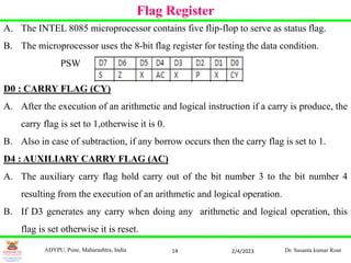
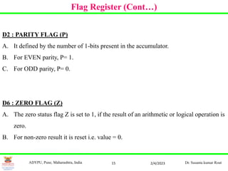
3. Additional documents provide details on the architecture, registers, flags, program counter, and stack pointer of the 8085 microprocessor.