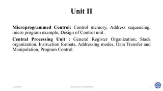
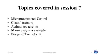
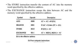
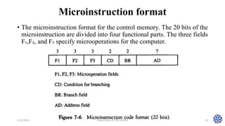
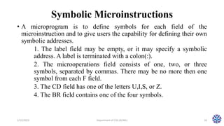
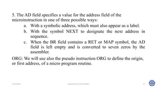
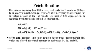
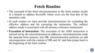
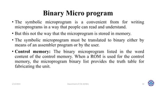
This document provides an overview of the topics covered in a session on computer organization and architecture. It discusses microprogrammed control, including control memory, address sequencing, and the design of the control unit. It provides an example of a microprogram, including the instruction format, microinstruction format, and a symbolic and binary representation of a fetch routine microprogram. The session covered microprogrammed control, control memory, address sequencing, an example microprogram, and the design of the control unit.
Computer engineering - overview of microprocessorsEkeedaPvtLtd
Computer engineering is a part of the Engineering and Technology course that deals with software and computers. It integrates different fields of computer and electronic engineering in order to develop computer software and hardware. The computer engineers are trained with both software and hardware related subjects so that they can understand and implement their knowledge in the real world too. The computer engineers have various opportunities when it comes to their career. The advancement in technology and the requirement of various software has paved a glorious path for computer engineers. From big MNCs to small startups, everyone is in need of a computer genius. Computer engineering mainly deals with microcontrollers and processors, circuit designing, designing personal as well as supercomputers, etc. This stream completely focuses on providing knowledge about both software and hardware for students.
A 16-bit microprocessor I designed during my final semester (2005) of my Bachelor of Technology program. The microprocessor circuitry design was coded in VHDL and then configured in a Xilinx XC9572 PC84 CPLD kit. Most of the design, the architecture and the instruction set were taken from Computer System Architecture (3rd ed.) by M. Morris Mano. See https://github.com/susam/mano-cpu for VHDL source code and other related files.
A Novel Architecture Design & Characterization of CAM Controller IP Core with...idescitation
Content Addressable Memory (CAM) is a special
purpose Random Access Memory device that can be accessed
by searching for data content. This paper describes a novel
architecture design and characterization of a reusable soft IP
core for CAM controller with sequential replacement policy,
so as to improve the match ratio of the CAM memory. The
proposed design was modeled using Verilog HDL and also
prototyped in Xilinx® SPARTAN family FPGA.The power
analysis was done using XPower® analyzer and the hardware
test result was obtained by ChipScope® Pro logic analyzer.
Index Terms—
Error Detection and Correction in SRAM Cell Using Decimal Matrix Codeiosrjce
Error Correction Codes (ECCs) are commonly used to protect memories from soft errors. As
technology scales, Multiple Cell Upsets (MCUs) become more common and affect a larger number of cells. To
prevent the occurrence of MCUs several error correction codes (ECCs) are used, but the main problem is that
they require complex encoder and decoder architecture and higher delay overheads. The decimal matrix code
(DMC) minimizes the area and delay overheads compared to the existing codes such as hamming, RS codes and
also improves the memory reliability by enhancing the error correction capability. In this paper, novel
decimal matrix code (DMC) based on divide-symbol is proposed to enhance memory reliability with
lower delay overhead. The proposed DMC utilizes decimal algorithm to obtain the maximum error
detection capability. Moreover, the encoder-reuse technique (ERT) is proposed to minimize the area
overhead of extra circuits without disturbing the whole encoding and decoding processes. ERT uses DMC encoder itself to be part of the decoder.
Register Organization of 8086, Architecture, Signal Description of 8086, Physical Memory
Organization, General Bus Operation, I/O Addressing Capability, Special Processor Activities,
Minimum Mode 8086 System and Timings, Maximum Mode 8086 System and Timings.
Addressing Modes of 8086.
CCS335 _ Neural Networks and Deep Learning Laboratory_Lab Complete RecordAsst.prof M.Gokilavani
LIST OF EXPERIMENTS:
1. Implement simple vector addition in Tensor Flow.
2. Implement a regression model in Keras.
3. Implement a perception in TensorFlow/Keras Environment.
4. Implement a Feed Forward Network in TensorFlow/Keras.
5. Implement an image classifier using CNN in TensorFlow/Keras.
6. Improve the deep Learning model by fine tuning hyper parameters.
7. Implement a Transfer Learning concept in image classification.
8. Using a pre trained model on Keras for transfer learning.
9. Perform Sentimental Analysis using RNN.
10. Implement an LSTM based Auto encoding inTensorflow/Keras.
11. Image generation using GAN.
ADDITIONAL EXPERIMENTS
12. Train a deep Learning model to classify a given image using pre trained model.
13. Recommendation system from sales data using Deep Learning.
14. Implement Object detection using CNN.
15. Implement any simple Reinforcement Algorithm for an NLP problem.
CCS355 Neural Networks & Deep Learning Unit 1 PDF notes with Question bank .pdfAsst.prof M.Gokilavani
UNIT I INTRODUCTION
Neural Networks-Application Scope of Neural Networks-Artificial Neural Network: An IntroductionEvolution of Neural Networks-Basic Models of Artificial Neural Network- Important Terminologies of
ANNs-Supervised Learning Network.
KuberTENes Birthday Bash Guadalajara - K8sGPT first impressionsVictor Morales
K8sGPT is a tool that analyzes and diagnoses Kubernetes clusters. This presentation was used to share the requirements and dependencies to deploy K8sGPT in a local environment.
Online aptitude test management system project report.pdfKamal Acharya
The purpose of on-line aptitude test system is to take online test in an efficient manner and no time wasting for checking the paper. The main objective of on-line aptitude test system is to efficiently evaluate the candidate thoroughly through a fully automated system that not only saves lot of time but also gives fast results. For students they give papers according to their convenience and time and there is no need of using extra thing like paper, pen etc. This can be used in educational institutions as well as in corporate world. Can be used anywhere any time as it is a web based application (user Location doesn’t matter). No restriction that examiner has to be present when the candidate takes the test.
Every time when lecturers/professors need to conduct examinations they have to sit down think about the questions and then create a whole new set of questions for each and every exam. In some cases the professor may want to give an open book online exam that is the student can take the exam any time anywhere, but the student might have to answer the questions in a limited time period. The professor may want to change the sequence of questions for every student. The problem that a student has is whenever a date for the exam is declared the student has to take it and there is no way he can take it at some other time. This project will create an interface for the examiner to create and store questions in a repository. It will also create an interface for the student to take examinations at his convenience and the questions and/or exams may be timed. Thereby creating an application which can be used by examiners and examinee’s simultaneously.
Examination System is very useful for Teachers/Professors. As in the teaching profession, you are responsible for writing question papers. In the conventional method, you write the question paper on paper, keep question papers separate from answers and all this information you have to keep in a locker to avoid unauthorized access. Using the Examination System you can create a question paper and everything will be written to a single exam file in encrypted format. You can set the General and Administrator password to avoid unauthorized access to your question paper. Every time you start the examination, the program shuffles all the questions and selects them randomly from the database, which reduces the chances of memorizing the questions.
Harnessing WebAssembly for Real-time Stateless Streaming PipelinesChristina Lin
Traditionally, dealing with real-time data pipelines has involved significant overhead, even for straightforward tasks like data transformation or masking. However, in this talk, we’ll venture into the dynamic realm of WebAssembly (WASM) and discover how it can revolutionize the creation of stateless streaming pipelines within a Kafka (Redpanda) broker. These pipelines are adept at managing low-latency, high-data-volume scenarios.
Literature Review Basics and Understanding Reference Management.pptxDr Ramhari Poudyal
Three-day training on academic research focuses on analytical tools at United Technical College, supported by the University Grant Commission, Nepal. 24-26 May 2024
HEAP SORT ILLUSTRATED WITH HEAPIFY, BUILD HEAP FOR DYNAMIC ARRAYS.
Heap sort is a comparison-based sorting technique based on Binary Heap data structure. It is similar to the selection sort where we first find the minimum element and place the minimum element at the beginning. Repeat the same process for the remaining elements.
Water billing management system project report.pdfKamal Acharya
Our project entitled “Water Billing Management System” aims is to generate Water bill with all the charges and penalty. Manual system that is employed is extremely laborious and quite inadequate. It only makes the process more difficult and hard.
The aim of our project is to develop a system that is meant to partially computerize the work performed in the Water Board like generating monthly Water bill, record of consuming unit of water, store record of the customer and previous unpaid record.
We used HTML/PHP as front end and MYSQL as back end for developing our project. HTML is primarily a visual design environment. We can create a android application by designing the form and that make up the user interface. Adding android application code to the form and the objects such as buttons and text boxes on them and adding any required support code in additional modular.
MySQL is free open source database that facilitates the effective management of the databases by connecting them to the software. It is a stable ,reliable and the powerful solution with the advanced features and advantages which are as follows: Data Security.MySQL is free open source database that facilitates the effective management of the databases by connecting them to the software.
Hierarchical Digital Twin of a Naval Power SystemKerry Sado
A hierarchical digital twin of a Naval DC power system has been developed and experimentally verified. Similar to other state-of-the-art digital twins, this technology creates a digital replica of the physical system executed in real-time or faster, which can modify hardware controls. However, its advantage stems from distributing computational efforts by utilizing a hierarchical structure composed of lower-level digital twin blocks and a higher-level system digital twin. Each digital twin block is associated with a physical subsystem of the hardware and communicates with a singular system digital twin, which creates a system-level response. By extracting information from each level of the hierarchy, power system controls of the hardware were reconfigured autonomously. This hierarchical digital twin development offers several advantages over other digital twins, particularly in the field of naval power systems. The hierarchical structure allows for greater computational efficiency and scalability while the ability to autonomously reconfigure hardware controls offers increased flexibility and responsiveness. The hierarchical decomposition and models utilized were well aligned with the physical twin, as indicated by the maximum deviations between the developed digital twin hierarchy and the hardware.
CS304PC:Computer Organization and Architecture session 9 microprogram example.pptx
1. CS304PC:Computer Organization
and Architecture (R18 II(I sem))
Department of computer science and engineering
(AI/ML)
Session 9
by
Asst.Prof.M.Gokilavani
VITS
1/12/2023 Department of CSE (AI/ML) 1
2. TEXTBOOK:
• 1. Computer System Architecture – M. Moris Mano, Third Edition,
Pearson/PHI.
REFERENCES:
• Computer Organization – Car Hamacher, Zvonks Vranesic, Safea
Zaky, Vth Edition, McGraw Hill.
• Computer Organization and Architecture – William Stallings Sixth
Edition, Pearson/PHI.
• Structured Computer Organization – Andrew S. Tanenbaum, 4th
Edition, PHI/Pearson.
1/12/2023 Department of CSE (AI/ML) 2
3. Unit II
Microprogrammed Control: Control memory, Address sequencing,
micro program example, Design of Control unit .
Central Processing Unit : General Register Organization, Stack
organization, Instruction formats, Addressing modes, Data Transfer and
Manipulation, Program Control.
1/12/2023 Department of CSE (AI/ML) 3
4. Topics covered in session 7
1/12/2023 Department of CSE (AI/ML) 4
• Microprogrammed Control
• Control memory
• Address sequencing
• Micro program example
• Design of Control unit
5. Micro program Example
• Once the configuration of a computer and its micro programmed
control unit is established, the designer’s task is to generate the
microcode foe the control memory.
• This code generation is called micro programming and is a process
similar to conventional machine language programming.
1/12/2023 Department of CSE (AI/ML) 5
6. Computer Hardware Configuration
• It consists of two memory units: a main memory for storing instruction
and data, and a control memory for storing the micro program.
• Four registers are associated with the processor unit and two with the
control unit.
• The processor registers are program counter PC, address register AR,
data register DR, and accumulator register AC.
• The control unit has a control address register CAR and a subroutine
register SBR.
• The control memory and its registers are organized as a
microprogrammed control units.
1/12/2023 Department of CSE (AI/ML) 6
8. Instruction Format
• It consists of three fields: a 1-bit field for indirect addressing
symbolized by I me, a 4-bit operation code(opcode), and an 11-bit
address field.
• Lists of four of the 16 possible memory-reference instructions.
• The ADD instruction adds the content of the operand found in the
effective address to the content of AC.
• The BRANCH instruction causes a branch to the effective address if
the operand in AC is negative.
1/12/2023 Department of CSE (AI/ML) 8
9. • The STORE instruction transfer the content of AC into the memory
word specified by the effective address.
• The EXCHANGE instruction swaps the data between AC and the
memory word specified by the affective address.
1/12/2023 Department of CSE (AI/ML) 9
10. Microinstruction format
• The microinstruction format for the control memory. The 20 bits of the
microinstruction are divided into four functional parts. The three fields
F₁,F₂, and F₃ specify microoperations for the computer.
1/12/2023 Department of CSE (AI/ML) 10
11. i. Microoperations: The microoperations are subdivided into three
fields of three bits each.
• The three bits in each field are encoded to specify seven distinct
microoperations.
• This gives a total of 21 micro-operations.
• No more than three micro-operations can be chosen for a
microinstruction, one from each field.
• If fewer than three micro-operations are used, one or more of
the fields will use the binary code 000 for no operation.
• As an illustration, a microinstruction can specify two
simultaneous micro-operations from F2 and F3 and none
from F1.
1/12/2023 Department of CSE (AI/ML) 11
12. • Each micro-operation in Table is defined with a register transfer
statement and is assigned a symbol for use in a symbolic microprogram.
•All transfer-type micro-operations symbols use five letters. The first two
letters designate the source register, the third letter is always a T, and the
last two letters designate the destination register.
•For example, the micro-operation that specifies the transfer
has the symbol DRTAC, which stands for a transfer from DR to AC.
1/12/2023 Department of CSE (AI/ML) 12
13. ii. Condition field: The CD field consists of two bits which are encoded
to specify four status bit conditions. The first condition is always a 1, so
that a reference to CD=00 will always find the condition to be true.
1/12/2023 Department of CSE (AI/ML) 13
14. iii. Branch field: The BR field consists of two bits. It is used, in
conjunction with the address field AD, to choose the address of the next
microinstruction. When BR=00, the control performs a jump(JMP)
operation, and when BR=01, it performs a call to subroutine operation.
1/12/2023 Department of CSE (AI/ML) 14
15. Each of the three microoperation fields can specify one of seven possibilities.
No more than three microoperations can be chosen for a microinstruction.
If fewer than three are needed, the code 000 = NOP.
The three bits in each field are encoded to specify seven distinct microoperations listed
in below table.
1/12/2023 Department of CSE (AI/ML) 15
16. Symbolic Microinstructions
• A microprogram is to define symbols for each field of the
microinstruction and to give users the capability for defining their own
symbolic addresses.
1. The label field may be empty, or it may specify a symbolic
address. A label is terminated with a colon(:).
2. The microoperations field consists of one, two, or three
symbols, separated by commas. There may be no more then one
symbol from each F field.
3. The CD field has one of the letters U,I,S, or Z.
4. The BR field contains one of the four symbols.
1/12/2023 Department of CSE (AI/ML) 16
17. 5. The AD field specifies a value for the address field of the
microinstruction in one of three possible ways:
a. With a symbolic address, which must also appear as a label.
b. With the symbol NEXT to designate the next address in
sequence.
c. When the BR field contains a RET or MAP symbol, the AD
field is left empty and is converted to seven zeros by the
assembler.
ORG: We will use also the pseudo instruction ORG to define the origin,
or first address, of a micro program routine.
1/12/2023 Department of CSE (AI/ML) 17
18. Fetch Routine
• The control memory has 128 words, and each word contains 20 bits.
To microprogram the control memory, it is necessary to determine the
bit values of each of the 128 words. The first 64 bits words are to be
occupied by the routines for the 16 instruction.
• Fetch and decode: The fetch routine needs three microinstructions,
which are placed in control memory at addresses 64, 65, and 66.
1/12/2023 Department of CSE (AI/ML) 18
19. Fetch Routine
• The executed of the third microinstruction in the fetch routine results
in a branch to address 0xxxx00, where xxxx are the four bits of the
operation code.
• In each routine we must provide microinstruction for evaluating the
effective address and for executing the instruction. The indirect
address mode is associated with all memory-reference instructions.
• Execution of instruction: The execution of the ADD instruction is
carried out by the microinstruction at addresses. microinstruction reads
the operand from memory into DR. microinstruction performs an add
microoperation with the content of DR and AC and then jumps back to
the beginning of the fetch routine.
1/12/2023 Department of CSE (AI/ML) 19
20. Binary Micro program
• The symbolic microprogram is a convenient from for writing
microprograms in a way that people can read and understand.
• But this not the way that the microprogram is stored in memory.
• The symbolic microprogram must be translated to binary either by
means of an assembler program or by the user.
• Control memory: The binary microprogram listed in the word
content of the control memory. When a ROM is used for the control
memory, the microprogram binary list provides the truth table for
fabricating the unit.
1/12/2023 Department of CSE (AI/ML) 20
21. Topics to be covered in next session 10
• Design of Control Unit
1/12/2023 Department of CSE (AI/ML) 21
Thank you!!!