For any help regarding Semiconductor Assignment Help visit :
https://www.eduassignmenthelp.com, Email :-
info@eduassignmenthelp.com or call us at :- +1 678 648 4277
eduassignmenthelp.com
Problem 1 - Consider a metal-semiconductor junction formed between a metal with a work function of 4.0 eV, and a hypothetical
semiconductor with an energy gap, Eg, of
4.eV, an electron affinity of 3.5 eV, and a conduction band effective density of states of 1019
cm-3
, that is doped n-type with 1016
cm-3
donor
atoms (which you may assume are all ionized at room temperature).
a) What is the work function of this semiconductor sample? NOTE: For convenience you may assume that kT ln 10 = 0.06 eV at room
temperature.
b) What is the barrier height in this Schottky diode, and what is the depletion region width in thermal equilibrium, i.e., with zero bias?
Now consider that the semiconductor also has 1013
cm-2
surface states that are located
3.Eg above the edge of the valence band. Assume that these surface states are neutral when they are empty.
c) What is the condition of a bare surface of this semiconductor because of the presense of these surface states, that is, is it depleted,
accumulated, or unchanged? If it is depleted, what is the depletion region width and what fraction of the surface states are
occupied in thermal equilibrium?
Next return to the metal-semiconductor junction, now with the surface states present. Assume that the centroids of the charge layer at
the metal surface and of the charge in the surface states are separated by 20 nm.
d) What is the barrier height in this Schottky diode when there are surface states present, and what is the depletion region width in
thermal equilibrium? Also, what fraction of the surface states are occupied in thermal equilibrium?
Problem 2 - Develop a simple approximate expression for the reduction in the barrier height of a metal-semiconductor junction caused by
image force lowering. Discuss the functional dependance of the decrease on the doping level, Nd, and the barrier height without
lowering, i.e. Bo.
Problem 3 - Compare the saturation current, IS, of a metal-semiconductor diode on n- type silicon, Nd = 1017 cm-3, with that of a p-n
junction diode made on the same n-type Si using p-type silicon with (a) Na = 1018 cm-3 and (b) Na = 1016 cm-3. Assume infinite
minority carrier lifetime, n- and p-region lengths of 1 µm each (you may neglect the depletion region widths in your calculations), a
low-field electron mobility, µe, of 1600
COMPOUND SEMICONDUCTOR DEVICES
Problems
eduassignmenthelp.com
cm2/V-s, a low-field hole mobility, µh, of 600 cm2/V-s, an intrinsic carrier concentraion, ni, of 1010 cm-3, and a barrier height, qB,
of 0.7 eV for the metal-semiconductor barrier. Use the thermoinic emission model for the Schottky diode current.
Problem 4 - Reading is FUNdamental:
a) Look up the following reference: Applied Physics Letters, Vol. 80 (27 May 2002), pp. 3967-3969.
i) What new do they report?
ii) What measurements did they use to reach their conclusions?
iii) Why should anyone care?
b) Consider the ternary compound GaNxAs1-x. For x small it crystallizes in the zinc blende lattice, just like GaAs.
i) Based on our discussion in Lecture 1, how would you expect the energy gap of this material to vary with x, for x small
(i.e., near GaAs)?
ii) Look in the literature and find out how the energy gap of this material varies with x, for small x. You might find it easier to
also look for information on Ga1-yInyNxAs1-x, which is very similar for y small. State what reference(s) you use.
c) Find a text that explains velocity saturation in semiconductors and give a 25 to 50 word synopsis of the arguement. Include
your source.
eduassignmenthelp.com
Solutions
Problem 1
Condition of the surface: The surface is depleted. The states are acceptor-like because the
states are neutral when unoccupied: the sites can hold static charges only if the electrons
occupy these states. Electrons from the surrounding area are drawn away from the surrounding
areas to fill these states, depleting the area of free carriers.
eduassignmenthelp.com
Problem 2
eduassignmenthelp.com
Problem 3
Problem 4
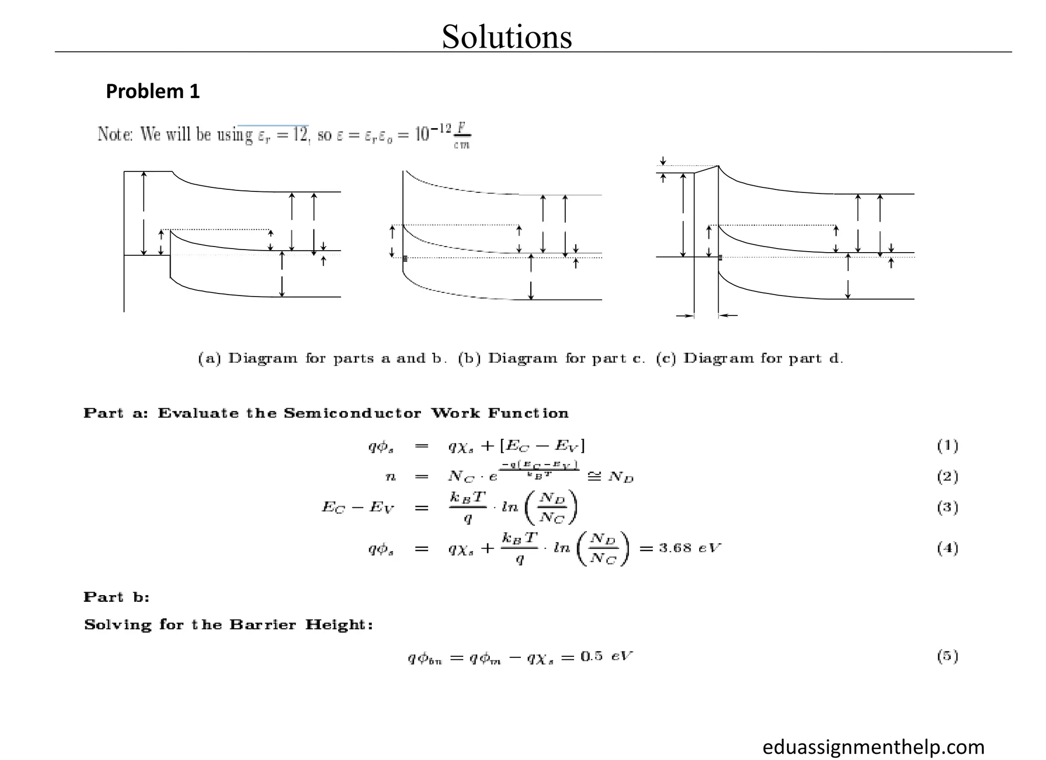
Part a: I: What are they reporting? They are reporting that the band gap for InN is between 0.7
and 0.8 eV.
ii. What measurements do they use? They used three different measurement techniques: optical
absorption, photoluminescence, and photomodulated reflection.
iii. Why are the results important? Most books and articles use 1.9 eV as the band gap for in N.
for both the wurtzite and zinc-blende lattice. If their claim is valid, this discovery changes our
understanding, processing, and modeling of the material, . A fairly recent article reported the
band gaps as 1.1 eV[3].
eduassignmenthelp.com
where the so-called bowing parameter C accounts for the deviation from a linear interpolation
(virtual-crystal approximation) between the two binaries A and B. The bowing parameter for 111-V
alloys is typically positive (i.e., the alloy band gap is smaller than the linear interpolation result)
and can in principle be a function of temperature. The physical origin of the band gap bowing can
be traced to the disorder effects caused by the presence of different cation (anions)[4].
Part c:
Write a 25-50 word synopsis of velocity saturation: Scattering of low kinetic energy carriers transfers
the energy to the lattice and generates acoustical phonons. Carriers subjected to high electric fields
obtain a large kinetic energy and scattering produces optical phonons. Generating optical phonons is
an effective method of transferring the carrier's kinetic energy to the lattice, and is the main cause
of velocity saturation.
eduassignmenthelp.com

Semiconductor Assignment Help

  • 1.
    For any helpregarding Semiconductor Assignment Help visit : https://www.eduassignmenthelp.com, Email :- info@eduassignmenthelp.com or call us at :- +1 678 648 4277 eduassignmenthelp.com
  • 2.
    Problem 1 -Consider a metal-semiconductor junction formed between a metal with a work function of 4.0 eV, and a hypothetical semiconductor with an energy gap, Eg, of 4.eV, an electron affinity of 3.5 eV, and a conduction band effective density of states of 1019 cm-3 , that is doped n-type with 1016 cm-3 donor atoms (which you may assume are all ionized at room temperature). a) What is the work function of this semiconductor sample? NOTE: For convenience you may assume that kT ln 10 = 0.06 eV at room temperature. b) What is the barrier height in this Schottky diode, and what is the depletion region width in thermal equilibrium, i.e., with zero bias? Now consider that the semiconductor also has 1013 cm-2 surface states that are located 3.Eg above the edge of the valence band. Assume that these surface states are neutral when they are empty. c) What is the condition of a bare surface of this semiconductor because of the presense of these surface states, that is, is it depleted, accumulated, or unchanged? If it is depleted, what is the depletion region width and what fraction of the surface states are occupied in thermal equilibrium? Next return to the metal-semiconductor junction, now with the surface states present. Assume that the centroids of the charge layer at the metal surface and of the charge in the surface states are separated by 20 nm. d) What is the barrier height in this Schottky diode when there are surface states present, and what is the depletion region width in thermal equilibrium? Also, what fraction of the surface states are occupied in thermal equilibrium? Problem 2 - Develop a simple approximate expression for the reduction in the barrier height of a metal-semiconductor junction caused by image force lowering. Discuss the functional dependance of the decrease on the doping level, Nd, and the barrier height without lowering, i.e. Bo. Problem 3 - Compare the saturation current, IS, of a metal-semiconductor diode on n- type silicon, Nd = 1017 cm-3, with that of a p-n junction diode made on the same n-type Si using p-type silicon with (a) Na = 1018 cm-3 and (b) Na = 1016 cm-3. Assume infinite minority carrier lifetime, n- and p-region lengths of 1 µm each (you may neglect the depletion region widths in your calculations), a low-field electron mobility, µe, of 1600 COMPOUND SEMICONDUCTOR DEVICES Problems eduassignmenthelp.com
  • 3.
    cm2/V-s, a low-fieldhole mobility, µh, of 600 cm2/V-s, an intrinsic carrier concentraion, ni, of 1010 cm-3, and a barrier height, qB, of 0.7 eV for the metal-semiconductor barrier. Use the thermoinic emission model for the Schottky diode current. Problem 4 - Reading is FUNdamental: a) Look up the following reference: Applied Physics Letters, Vol. 80 (27 May 2002), pp. 3967-3969. i) What new do they report? ii) What measurements did they use to reach their conclusions? iii) Why should anyone care? b) Consider the ternary compound GaNxAs1-x. For x small it crystallizes in the zinc blende lattice, just like GaAs. i) Based on our discussion in Lecture 1, how would you expect the energy gap of this material to vary with x, for x small (i.e., near GaAs)? ii) Look in the literature and find out how the energy gap of this material varies with x, for small x. You might find it easier to also look for information on Ga1-yInyNxAs1-x, which is very similar for y small. State what reference(s) you use. c) Find a text that explains velocity saturation in semiconductors and give a 25 to 50 word synopsis of the arguement. Include your source. eduassignmenthelp.com
  • 4.
  • 5.
    Condition of thesurface: The surface is depleted. The states are acceptor-like because the states are neutral when unoccupied: the sites can hold static charges only if the electrons occupy these states. Electrons from the surrounding area are drawn away from the surrounding areas to fill these states, depleting the area of free carriers. eduassignmenthelp.com
  • 6.
  • 7.
  • 8.
  • 9.
  • 10.
    Problem 4 Part a:I: What are they reporting? They are reporting that the band gap for InN is between 0.7 and 0.8 eV. ii. What measurements do they use? They used three different measurement techniques: optical absorption, photoluminescence, and photomodulated reflection. iii. Why are the results important? Most books and articles use 1.9 eV as the band gap for in N. for both the wurtzite and zinc-blende lattice. If their claim is valid, this discovery changes our understanding, processing, and modeling of the material, . A fairly recent article reported the band gaps as 1.1 eV[3]. eduassignmenthelp.com
  • 11.
    where the so-calledbowing parameter C accounts for the deviation from a linear interpolation (virtual-crystal approximation) between the two binaries A and B. The bowing parameter for 111-V alloys is typically positive (i.e., the alloy band gap is smaller than the linear interpolation result) and can in principle be a function of temperature. The physical origin of the band gap bowing can be traced to the disorder effects caused by the presence of different cation (anions)[4]. Part c: Write a 25-50 word synopsis of velocity saturation: Scattering of low kinetic energy carriers transfers the energy to the lattice and generates acoustical phonons. Carriers subjected to high electric fields obtain a large kinetic energy and scattering produces optical phonons. Generating optical phonons is an effective method of transferring the carrier's kinetic energy to the lattice, and is the main cause of velocity saturation. eduassignmenthelp.com