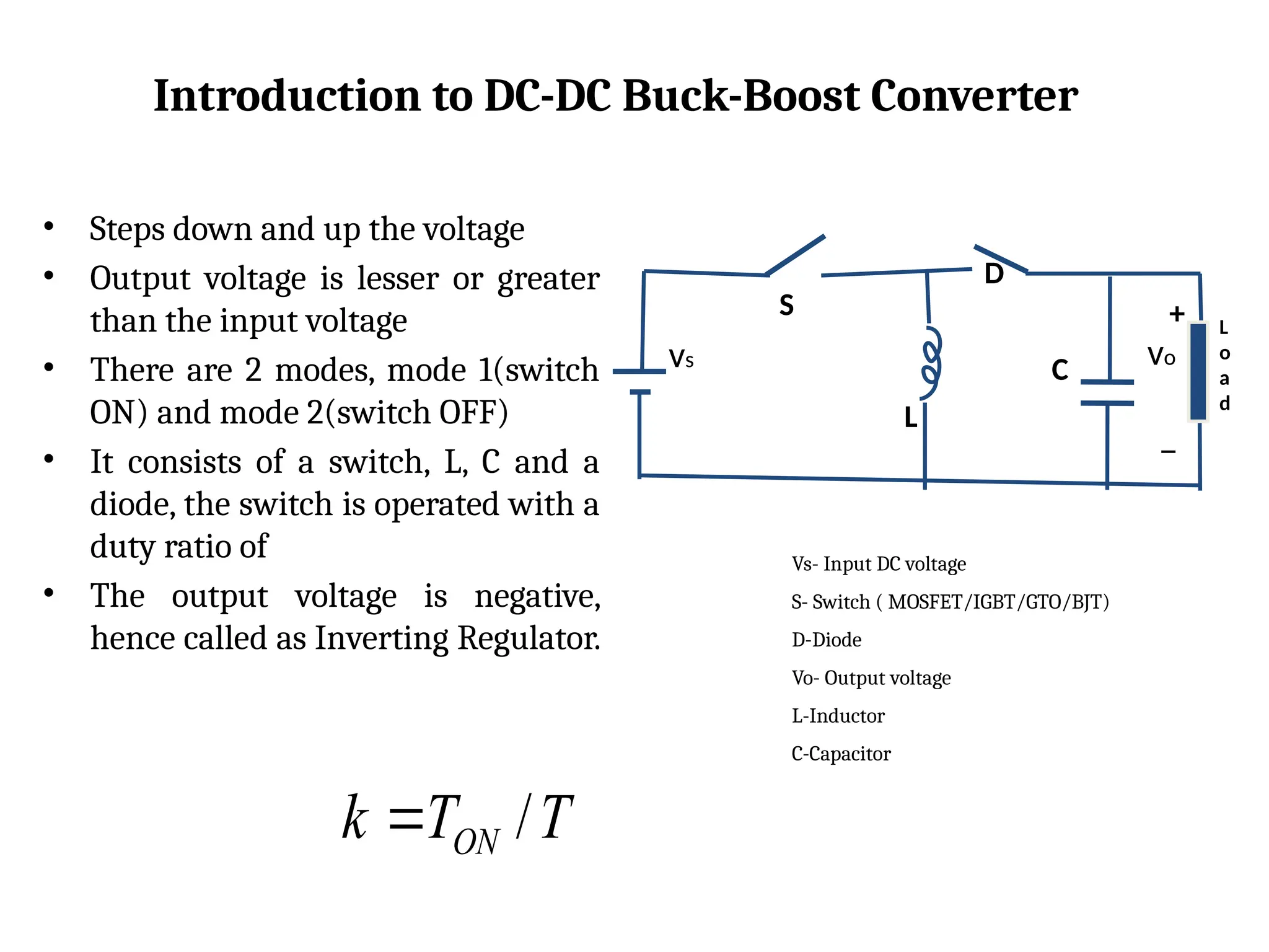
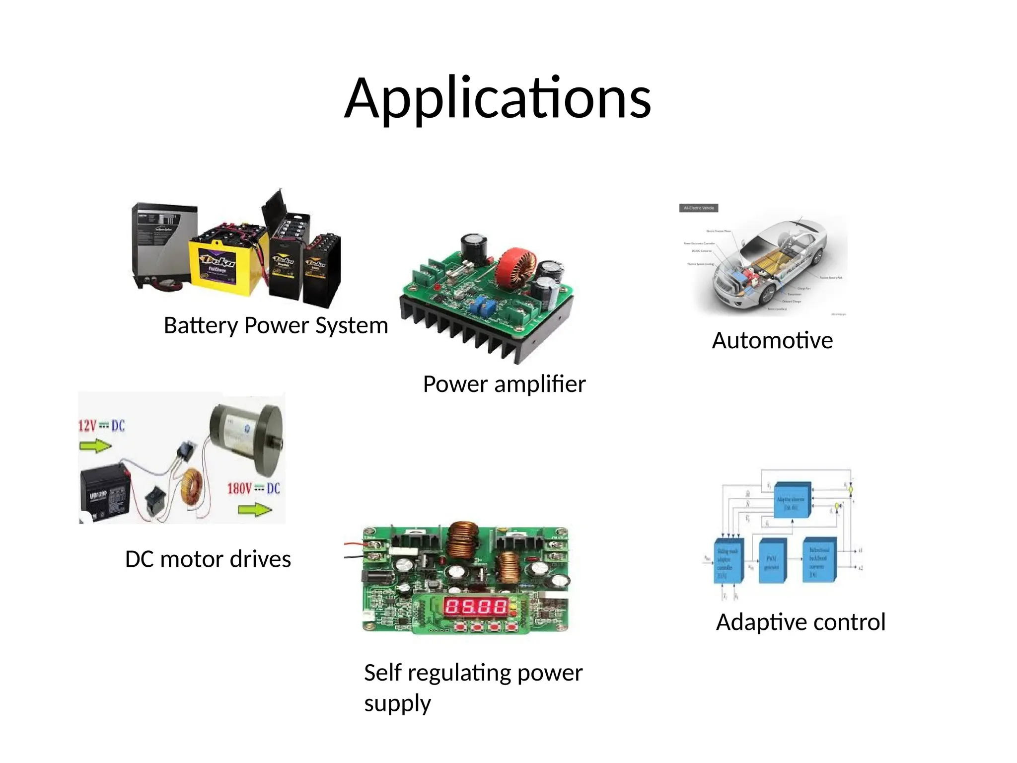
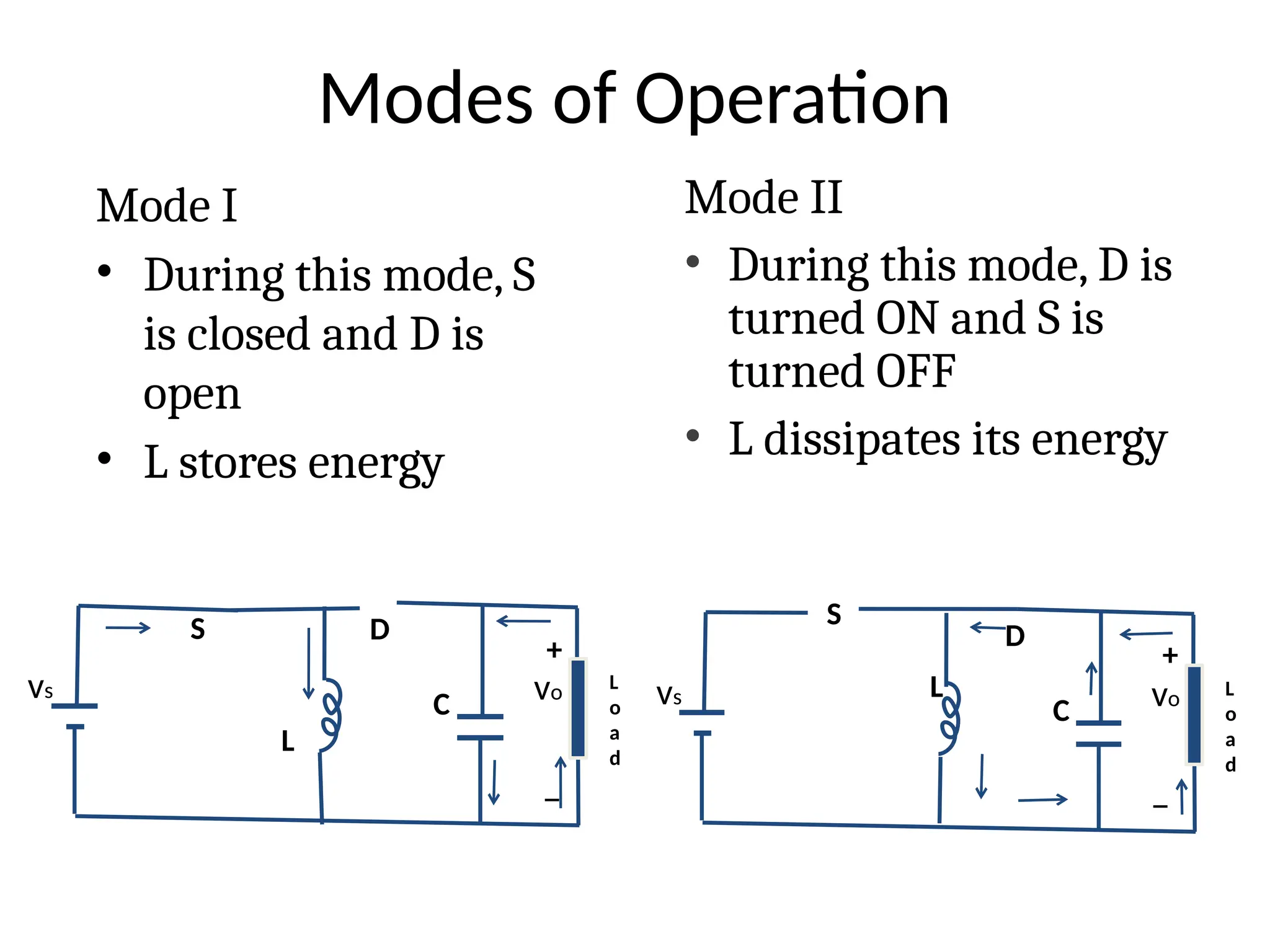
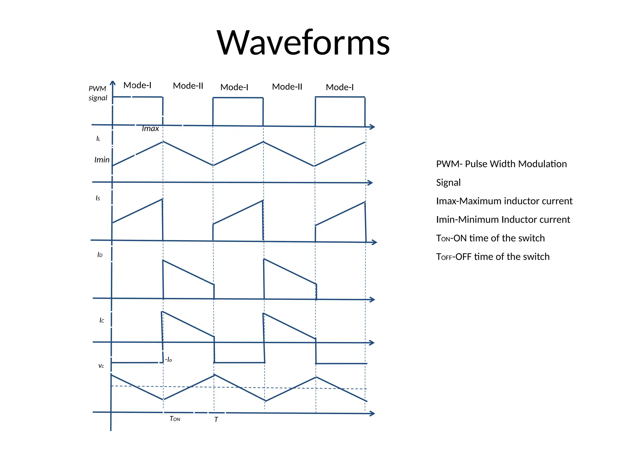
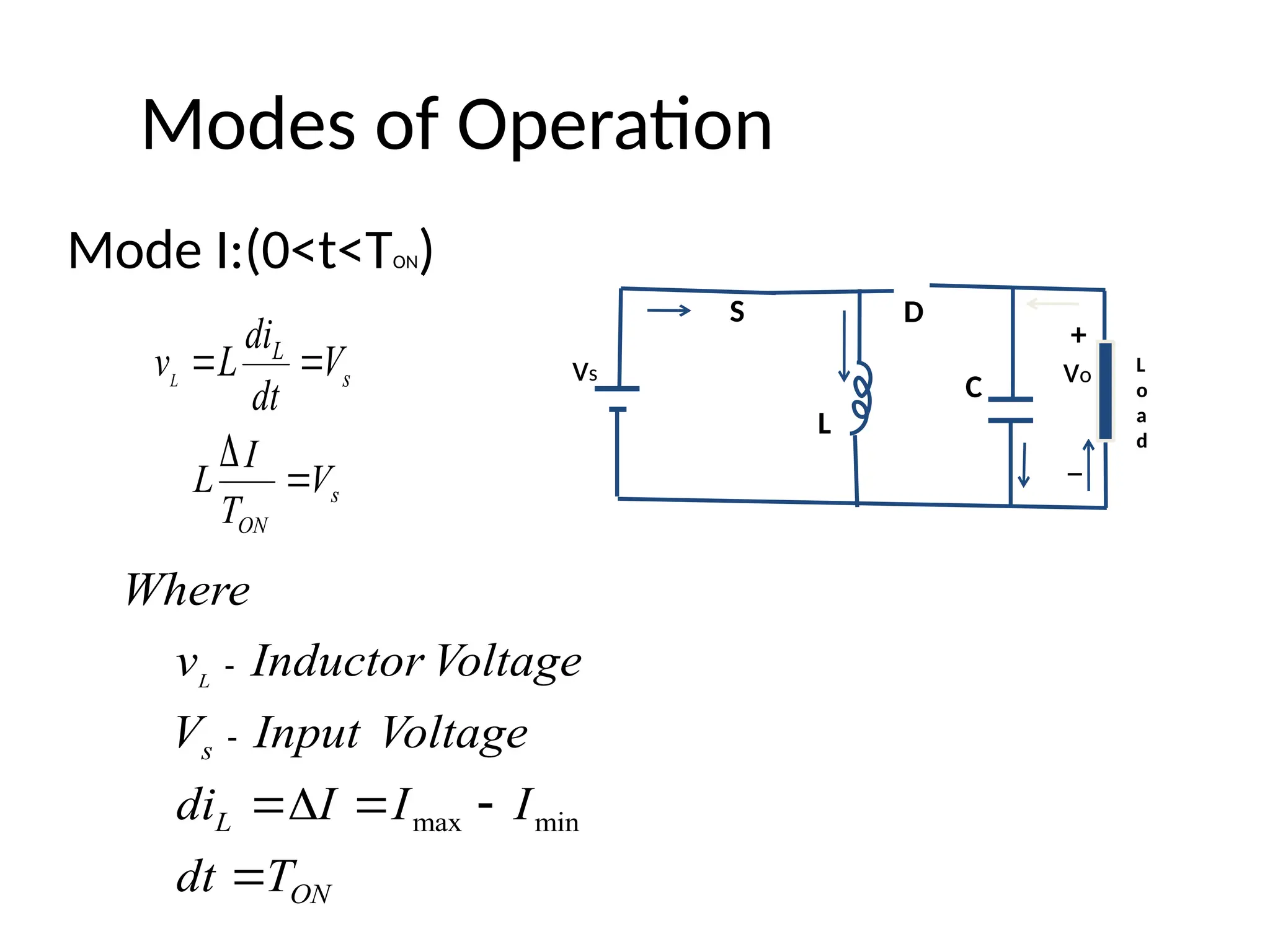
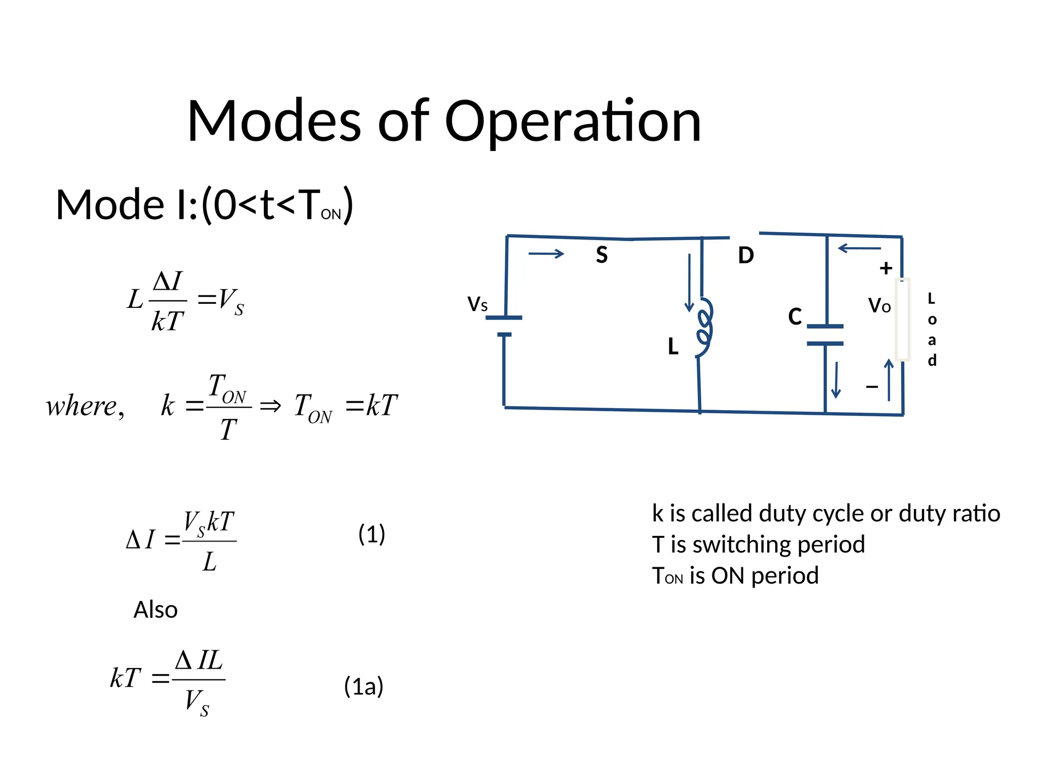
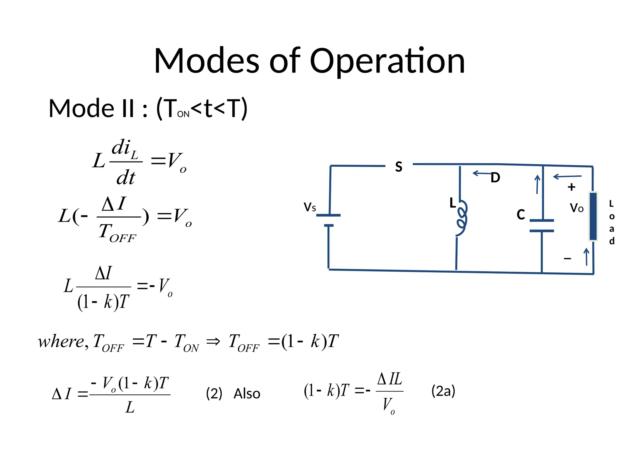
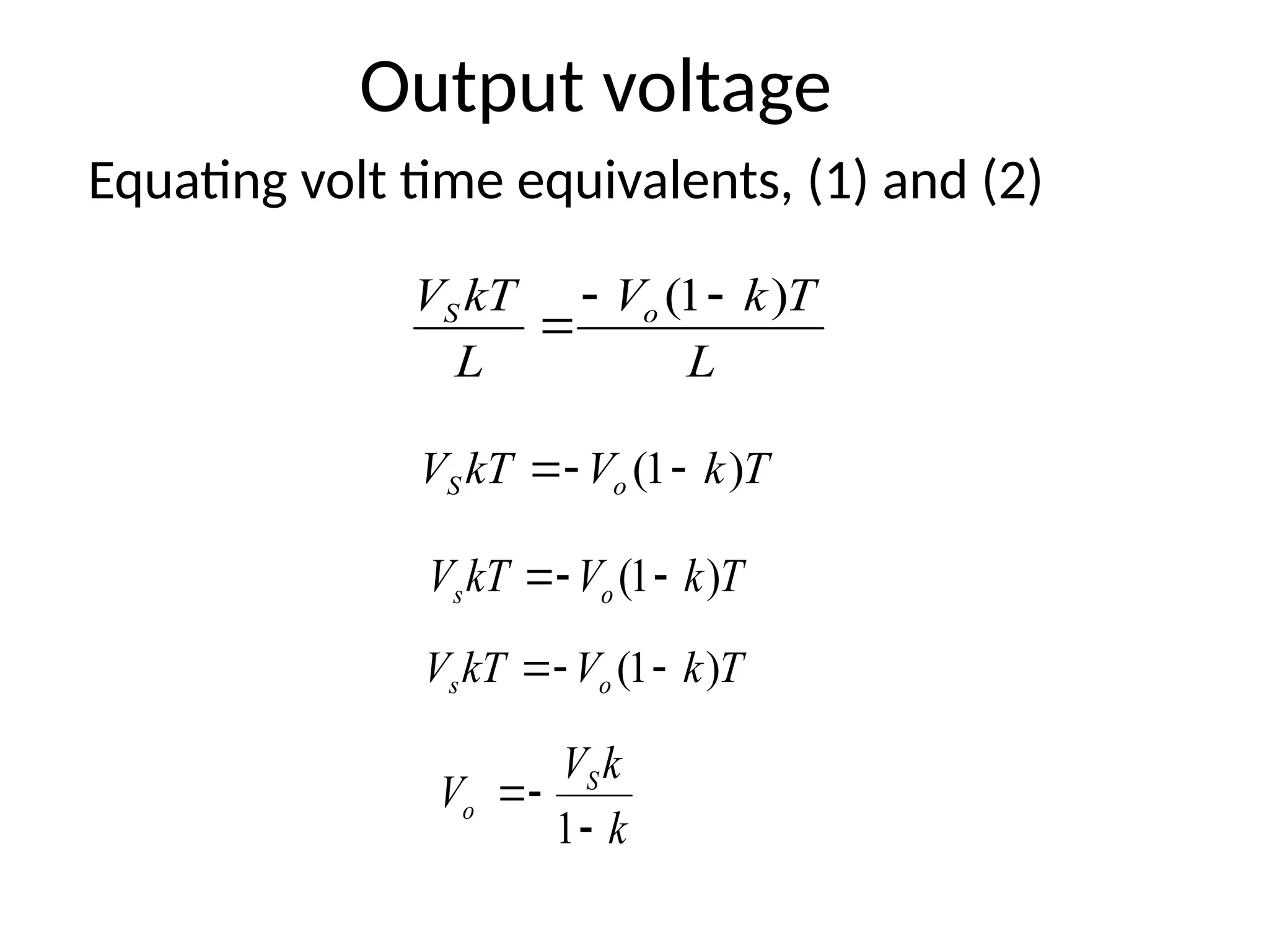
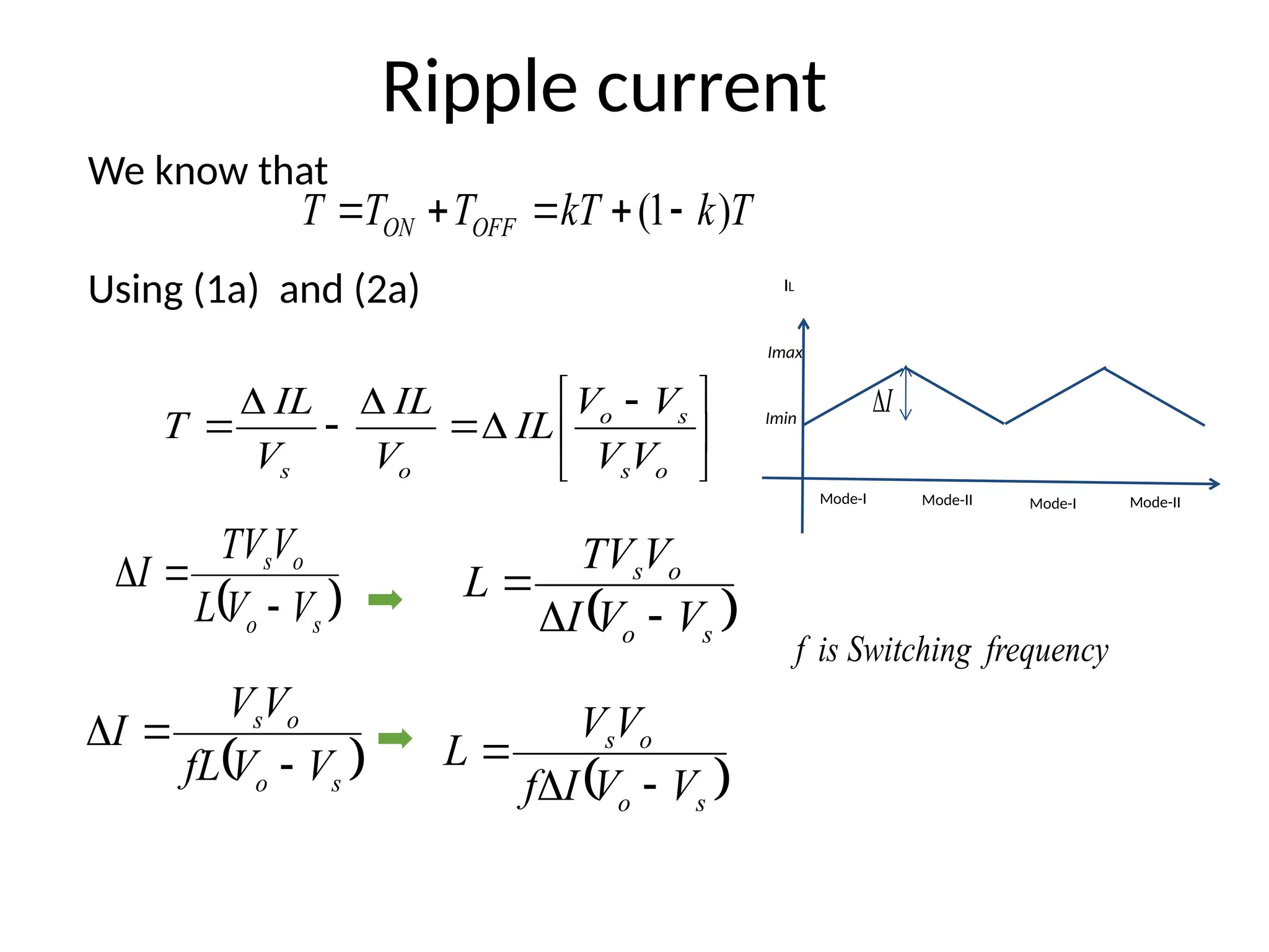
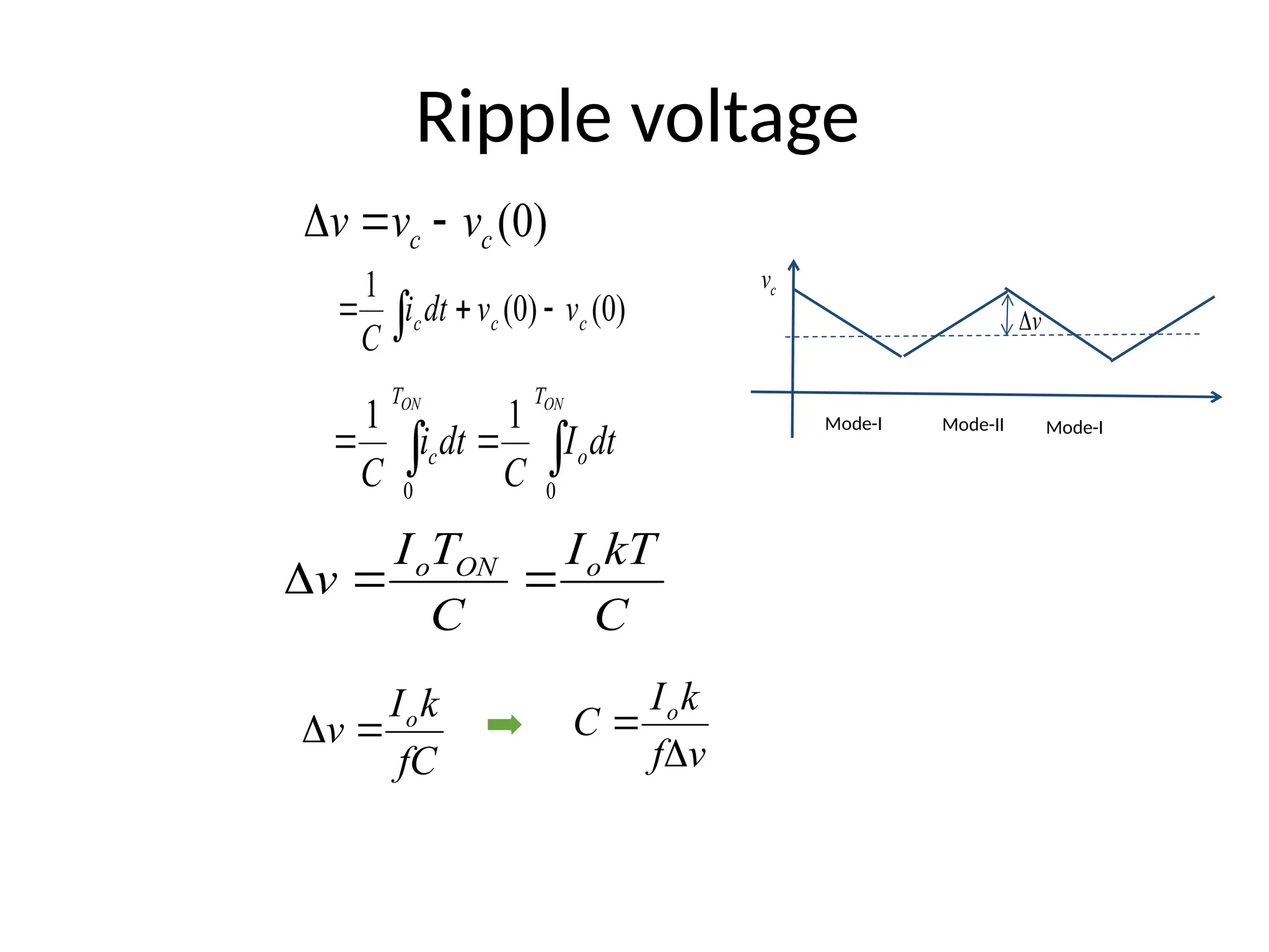
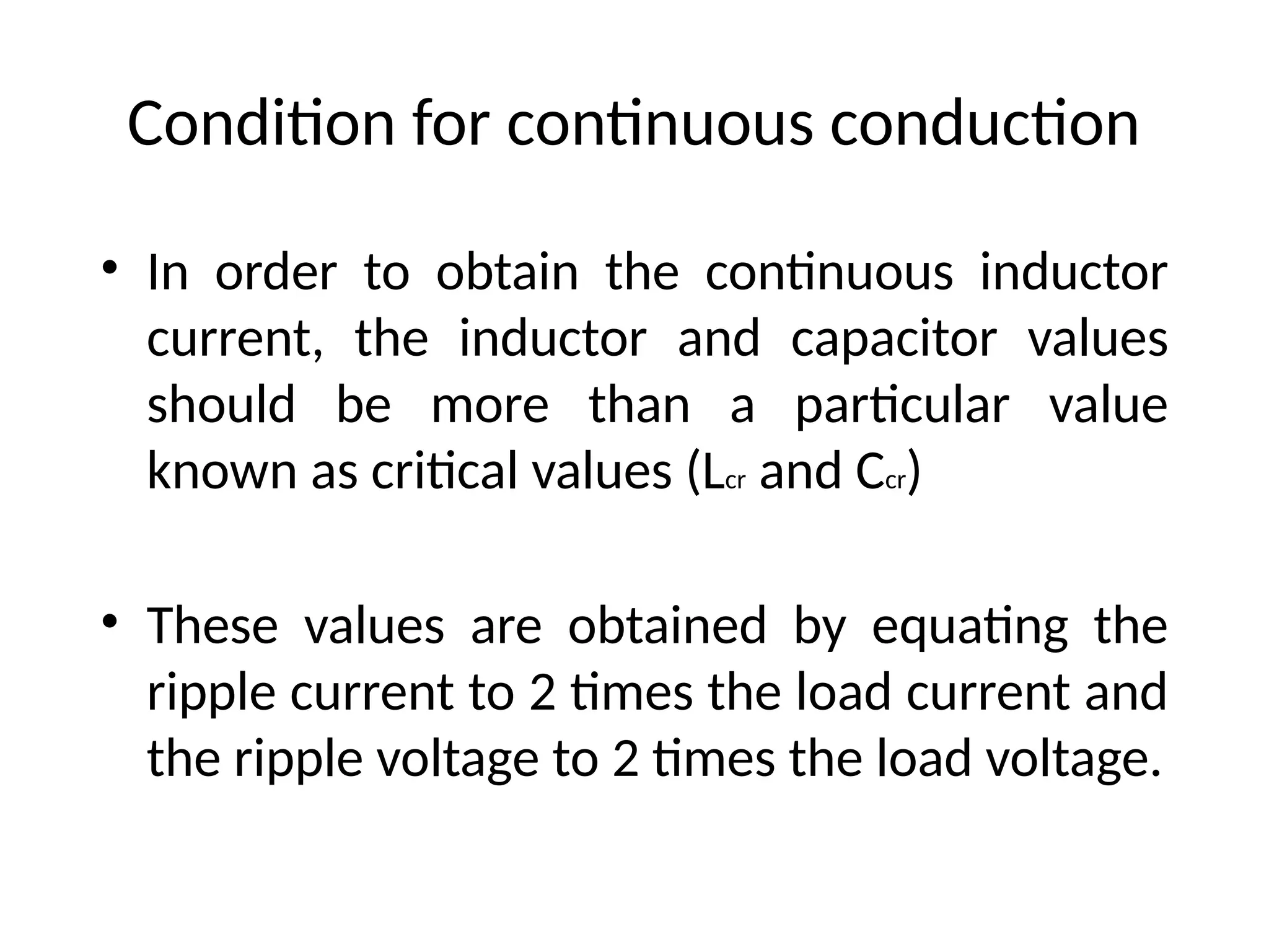
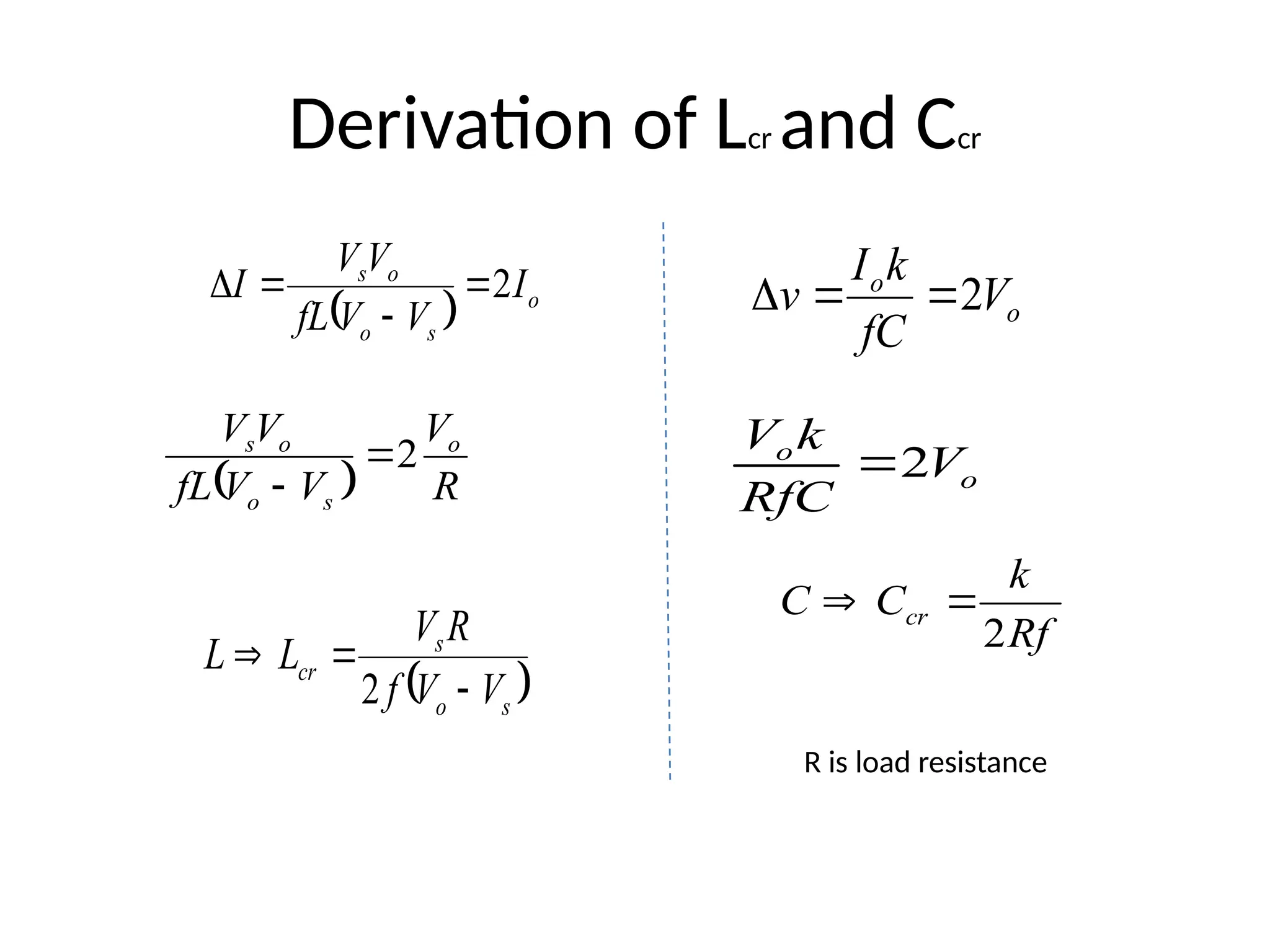
Introduction to DC-DC Buck-Boost Converter
• Steps down and up the voltage
• Output voltage is lesser or greater
than the input voltage
• There are 2 modes, mode 1(switch
ON) and mode 2(switch OFF)
• It consists of a switch, L, C and a
diode, the switch is operated with a
duty ratio of
• The output voltage is negative,
hence called as Inverting Regulator.
T
T
k ON /

vs vo
+
_
D
S
L
C
L
o
a
d
Vs- Input DC voltage
S- Switch ( MOSFET/IGBT/GTO/BJT)
D-Diode
Vo- Output voltage
L-Inductor
C-Capacitor
Applications
Source: prodctodc.com
Source: roboticsandautomationnewscom
Source: prodctodc.com
Self regulating power
supply
Automotive
Power amplifier
Adaptive control
Source: go.gale.com
Battery Power System
Source: bpsbattery.com
DC motor drives
Source: myoutube.com
Modes of Operation
Mode I
• During this mode, S
is closed and D is
open
• L stores energy
Mode II
• During this mode, D is
turned ON and S is
turned OFF
• L dissipates its energy
vs vo
+
_
D
S
L
C
L
o
a
d
vs vo
+
_
D
S
L
C
L
o
a
d
Waveforms
Mode-I Mode-II Mode-I Mode-I
Mode-II
Imin
Imax
PWM
signal
IL
IS
ID
IC
vc
TON T
-Io
PWM- Pulse Width Modulation
Signal
Imax-Maximum inductor current
Imin-Minimum Inductor current
TON-ON time of the switch
TOFF-OFF time of the switch
Modes of Operation
Mode I:(0<t<TON)
s
L
V
dt
di
L
vL


s
ON
V
T
I
L 

ON
L
s
T
dt
I
I
I
di
Voltage
Input
V
Voltage
Inductor
v
Where
L







min
max
vs vo
+
_
D
S
L
C
L
o
a
d
Modes of Operation
Mode I:(0<t<TON)
(1)
S
V
kT
I
L 

L
kT
V
I S


kT
T
T
T
k
where ON
ON



,
S
V
IL
kT

 (1a)
Also
k is called duty cycle or duty ratio
T is switching period
TON is ON period
vs vo
+
_
D
S
L
C
L
o
a
d
Modes of Operation
Mode II : (TON<t<T)
(2) Also
o
L
V
dt
di
L 
o
OFF
V
T
I
L 
 )
(

o
V
T
k
I
L 



)
1
(
L
T
k
V
I o )
1
( 



T
k
T
T
T
T
where OFF
ON
OFF )
1
(
, 




o
V
IL
T
k



 )
1
( (2a)
vs vo
+
_
D
S
L
C
L
o
a
d
Output voltage
Equating volt time equivalents, (1) and (2)
L
T
k
V
L
kT
V o
S )
1
( 


k
k
V
V S
o



1
T
k
V
kT
V o
S )
1
( 


T
k
V
kT
V o
s )
1
( 


T
k
V
kT
V o
s )
1
( 


Ripple current
We know that
Using (1a) and (2a)
T
k
kT
T
T
T OFF
ON )
1
( 









 






o
s
s
o
o
s V
V
V
V
IL
V
IL
V
IL
T
 
s
o
o
s
V
V
L
V
TV
I



Imin
Imax
Mode-I Mode-II Mode-I Mode-II
IL
I

frequency
Switching
is
f
 
s
o
o
s
V
V
I
V
TV
L



 
s
o
o
s
V
V
fL
V
V
I



 
s
o
o
s
V
V
I
f
V
V
L



Ripple voltage
)
0
(
c
c v
v
v 


)
0
(
)
0
(
1
c
c
c v
v
dt
i
C


 
C
kT
I
C
T
I
v o
ON
o



fC
k
I
v o



 

ON
ON T
o
T
c dt
I
C
dt
i
C 0
0
1
1
v

c
v
Mode-I Mode-II Mode-I
v
f
k
I
C o


Condition for continuous conduction
• In order to obtain the continuous inductor
current, the inductor and capacitor values
should be more than a particular value
known as critical values (Lcr and Ccr)
• These values are obtained by equating the
ripple current to 2 times the load current and
the ripple voltage to 2 times the load voltage.
Derivation of Lcr and Ccr
o
o
V
fC
k
I
v 2



Rf
k
C
C cr
2


R is load resistance
o
o
V
RfC
k
V
2

  o
s
o
o
s
I
V
V
fL
V
V
I 2




  R
V
V
V
fL
V
V o
s
o
o
s
2


 
s
o
s
cr
V
V
f
R
V
L
L



2
Thank you

Principle and Operation of DC-DCBuck-Boost converter

  • 1.
    Introduction to DC-DCBuck-Boost Converter • Steps down and up the voltage • Output voltage is lesser or greater than the input voltage • There are 2 modes, mode 1(switch ON) and mode 2(switch OFF) • It consists of a switch, L, C and a diode, the switch is operated with a duty ratio of • The output voltage is negative, hence called as Inverting Regulator. T T k ON /  vs vo + _ D S L C L o a d Vs- Input DC voltage S- Switch ( MOSFET/IGBT/GTO/BJT) D-Diode Vo- Output voltage L-Inductor C-Capacitor
  • 2.
    Applications Source: prodctodc.com Source: roboticsandautomationnewscom Source:prodctodc.com Self regulating power supply Automotive Power amplifier Adaptive control Source: go.gale.com Battery Power System Source: bpsbattery.com DC motor drives Source: myoutube.com
  • 3.
    Modes of Operation ModeI • During this mode, S is closed and D is open • L stores energy Mode II • During this mode, D is turned ON and S is turned OFF • L dissipates its energy vs vo + _ D S L C L o a d vs vo + _ D S L C L o a d
  • 4.
    Waveforms Mode-I Mode-II Mode-IMode-I Mode-II Imin Imax PWM signal IL IS ID IC vc TON T -Io PWM- Pulse Width Modulation Signal Imax-Maximum inductor current Imin-Minimum Inductor current TON-ON time of the switch TOFF-OFF time of the switch
  • 5.
    Modes of Operation ModeI:(0<t<TON) s L V dt di L vL   s ON V T I L   ON L s T dt I I I di Voltage Input V Voltage Inductor v Where L        min max vs vo + _ D S L C L o a d
  • 6.
    Modes of Operation ModeI:(0<t<TON) (1) S V kT I L   L kT V I S   kT T T T k where ON ON    , S V IL kT   (1a) Also k is called duty cycle or duty ratio T is switching period TON is ON period vs vo + _ D S L C L o a d
  • 7.
    Modes of Operation ModeII : (TON<t<T) (2) Also o L V dt di L  o OFF V T I L   ) (  o V T k I L     ) 1 ( L T k V I o ) 1 (     T k T T T T where OFF ON OFF ) 1 ( ,      o V IL T k     ) 1 ( (2a) vs vo + _ D S L C L o a d
  • 8.
    Output voltage Equating volttime equivalents, (1) and (2) L T k V L kT V o S ) 1 (    k k V V S o    1 T k V kT V o S ) 1 (    T k V kT V o s ) 1 (    T k V kT V o s ) 1 (   
  • 9.
    Ripple current We knowthat Using (1a) and (2a) T k kT T T T OFF ON ) 1 (                   o s s o o s V V V V IL V IL V IL T   s o o s V V L V TV I    Imin Imax Mode-I Mode-II Mode-I Mode-II IL I  frequency Switching is f   s o o s V V I V TV L      s o o s V V fL V V I      s o o s V V I f V V L   
  • 10.
    Ripple voltage ) 0 ( c c v v v   ) 0 ( ) 0 ( 1 c c c v v dt i C     C kT I C T I v o ON o    fC k I v o       ON ON T o T c dt I C dt i C 0 0 1 1 v  c v Mode-I Mode-II Mode-I v f k I C o  
  • 11.
    Condition for continuousconduction • In order to obtain the continuous inductor current, the inductor and capacitor values should be more than a particular value known as critical values (Lcr and Ccr) • These values are obtained by equating the ripple current to 2 times the load current and the ripple voltage to 2 times the load voltage.
  • 12.
    Derivation of Lcrand Ccr o o V fC k I v 2    Rf k C C cr 2   R is load resistance o o V RfC k V 2    o s o o s I V V fL V V I 2       R V V V fL V V o s o o s 2     s o s cr V V f R V L L    2
  • 13.