
Recommended
More Related Content
Similar to Unit-1 . non isolated boost.pptx
Similar to Unit-1 . non isolated boost.pptx (20)
Recently uploaded
Recently uploaded (20)
Unit-1 . non isolated boost.pptx
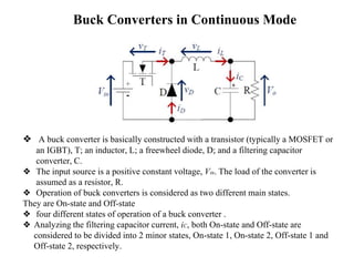
- 1. Buck Converters in Continuous Mode ❖ A buck converter is basically constructed with a transistor (typically a MOSFET or an IGBT), T; an inductor, L; a freewheel diode, D; and a filtering capacitor converter, C. ❖ The input source is a positive constant voltage, Vin. The load of the converter is assumed as a resistor, R. ❖ Operation of buck converters is considered as two different main states. They are On-state and Off-state ❖ four different states of operation of a buck converter . ❖ Analyzing the filtering capacitor current, iC, both On-state and Off-state are considered to be divided into 2 minor states, On-state 1, On-state 2, Off-state 1 and Off-state 2, respectively.
- 2. ❖ the function of the switching transistor, T, is for stepping down the voltage from Vin to Vo. ❖ Assuming all the components have no power loss, the average voltage across the freewheel diode, vD, is equal to the output voltage, Vo in steady state but its waveform is in the form of square wave. ❖ The inductor, L, and the filtering capacitor, C, form an L-C low-pass filter for filtering the ripple of vD. ❖ Assuming C is with very large capacitance, the output voltage, Vo, is constant. ❖ The freewheel diode, D, is for providing a current path for demagnetizing the inductor, L, to avoid saturation.
- 3. On-state 1 [t0 – t1] The switching transistor, T, is switched on at t0. During this state, the freewheel diode, D, is reverse biased. The inductor voltage, vL, is Vin – Vo. This causes L charged from the voltage source. The inductor current, iL, increases linearly. The current flows from the voltage source through L to the load, R. Since iL is lower than the output current, Vo/R, the filtering capacitor, C, discharges to R to keep the output voltage with low ripple. Its current, iC, increases to zero and iL increases to the output current at t1.
- 4. On-state 2 [t1 – t2] During this state, T is on and D is reverse biased. L is still being charged. iL is still increasing linearly. Since iL has become higher than the output current, Vo/R, C starts charged at t1 to keep Vo with low ripple and hence, iC increases linearly. Current flows from the voltage source through L to C and to R until T is switched off at t2.
- 5. Off-state 1 [t2 – t3] T is switched off at t2. D is forward biased. vL is equal to -Vo and hence L discharges in this state. iL decreases linearly. Since iL is still higher than the output current, C is charged from L to keep Vo with low ripple. Current flows from L through D to C and R. iC decreases to zero and iL decreases to the output current at t3.
- 6. Off-state 2 [t3 – t4] T is off, D is forward biased and L is discharging during this state. Since iL has become lower than the output current, C discharges to the load to keeps Vo with low ripple. Both iL and iC keeps decreasing linearly. Current flows from L through D to R. T is switched on again and one switching cycle is completed at t4.
- 7. Voltage Conversion Ratio of Buck Converters in Continuous Mode Equation of inductors is given as: vL in On-state and Off-state are both constants the changes of inductor current during On-state and Off-state are equal the voltage conversion ratio of a buck converter in continuous mode is Inductor Current of Buck Converters in Continuous Mode ❖ The voltage conversion ratio is linearly proportional to D. ❖ The voltage conversion ratio is in the range of 0 to 1. The output voltage is equal or lower than the input voltage. ❖ The voltage conversion ratio is independent of the load conditions. the average value of the inductor current Io is the average output current.
- 8. rms value of the inductor current voltage ripple to output voltage ratio is: cut-off frequency of the L-C filter is: switching frequency is: the output voltage ripple depends on the L and C product. Usually, L is selected to restrict the peak current of the converter and to prevent the converter to operate in discontinuous mode.
- 10. Boost Converters in Continuous Mode ❖ The function of boost converters is for stepping up the voltage. ❖ The circuit of a boost converter is basically constructed with a transistor, T; an inductor, L; a diode, D; and a filtering capacitor converter, C. ❖ The input voltage source is a positive constant voltage, Vin. The load of the converter is assumed as a resistor, R. ❖ Operation of boost converters is considered as two different states - On-state and Off-state. ❖ In On-state, the switching transistor of the converter, T, is on. In Off-state, T is off.
- 11. On-state [t0 – t1] The switching transistor, T, is switched on at t0. During this state, the diode, D, is reverse biased. The inductor voltage, vL, is Vin so that L is charged from the voltage source. The inductor current, iL, increases linearly. The current flows from the voltage source through L and T. The filtering capacitor, C, discharges to R to maintain the output voltage, Vo, with low ripple. Its current, iC, is equal to -Io, where Io is equal to Vo/R. T is switched off at t1.
- 12. Off-state [t1 – t2] T is switched off at t2. D is forward biased during this state. L demagnetizes and discharges to the load so that iL decreases linearly. iL is decreasing in this state so that vL is negative. Since the polarity of Vin and vL are the same, Vo must be equal to or higher than Vin. Current flow from Vin through L and D to C and R. C is charged. iC decreases linearly. T is switched on again and one switching cycle is completed at t2.
- 13. ❖ vL in On-state and Off-state of a boost converter are both constants. ❖ the changes of inductor current during On-state and Off-state are equal . ❖ D must be less than 1 otherwise short circuit occurs in the converter circuit. ❖ The voltage conversion ratio tends to infinity when D tends to 1. ❖ The voltage conversion ratio is in the range of 1 to almost infinity. The output voltage is equal to or less than the input voltage. ❖ The voltage conversion ratio is independent of the load conditions. Inductor Current of Boost Converters in Continuous Mode the average value of the inductor current is Io is the average output current rms value of the inductor current
- 15. Ćuk converter in Continuous Mode ❖ The function of Ćuk converters is for stepping up or down the voltage. ❖ The structure of a Ćuk converter is similar to the combination of a boost converter and a buck converter. ❖ Similar to buck-boost converters, the output voltage of Ćuk converters is inversed. ❖ It constructs with two inductors, L1 and L2; two capacitors, C1 and C2; one transistor, T; and one freewheel diode, D. ❖ The operation of Vin, L1, T1 and C1 is similar to a boost converter where C1 is like the output filtering capacitor. ❖ C1, L1, D1 and C2 is similar to a buck converter. ❖ It behaves as the load of the front boost converter part. C1 acts as the voltage source in this buck converter part. L2 and C2 build an L-C filter for the output. The main advantage of Ćuk converters is that the output filter is an L-C filter. The output current is continuous. The ripple of the filtering capacitor current and the output voltage lower is than that of buck-boost converters when they are using the same capacitors. Ćuk converters have more components than buck-boost converters. Also, the input current of this converter is also continuous so that the harmonics and electromagnetic interference are lower than those of buck-boost converters.
- 17. ❖ Operation of Ćuk converters is considered as two different main states. ❖ On-state and Off-state. ❖ In On-state, the switching transistor of the converter, T, is on. In Off-state, T is off. ❖ Analyzing the filtering capacitor current, iC, both On-state and Off-state are considered to be divided into 2 minor states, On-state 1, On- state 2, Off-state 1 and Off-state 2, respectively. ❖ Assuming C1 and C2 are with very high capacitance and the voltage across C1 and C2, VC1 and Vo respectively, are constant, each state of operation in steady state of a buck-boost converter. ❖ C1 discharges to R through L2. iL2 increases linearly. Maintaining the output voltage with low ripple, C2 discharges to the load as well. iC2 is negative and increases linearly. ❖ This behaves as a buck converter in On-state 1 while C1 acts as the voltage source. iC2, increases linearly until zero and iL1 increases to reach the output current, Io, at t1.
- 18. On-state 1 [t0 – t1] The switching transistor, T, is switched on at t0. D is reverse biased since vC1 is positive. vL is equal to Vin so that L1 is charged from Vin. iL1, increases linearly. It flows from Vin through L and T. C1 discharges and iC1 decreases linearly. This is like a boost converter in On-state. On-state 2 [t1 – t2] During this state, T is on and D is reverse biased. L1 is still being charged and iL1 is still increasing linearly. C1 is still discharging. Similar to On-state 1, this behaves as a boost converter in On-state. C1 is discharging to R and C2 through L2. iL2 is still increasing linearly. Since iL2 has become higher than Io, C2 starts charged at t1 to keep Vo with low ripple and hence, iC2 is positive and increases linearly. This behaviour is similar to a buck converter in On-state 2 while C1 acts as the voltage source. T is switched off at t2.
- 19. Off-state 1 [t2 – t3] T is switched off at t2. D is forward biased in this state. Because VC1 is higher than Vin, L1 discharges in this state and iL1 decreases linearly. C1 is charged from Vin through L1. iL1 flows from Vin through L1, V and D. It behaves as a boost converter in Off-state. Since iL2 is still higher than Io, C2 is still being charged from L2 to keep Vo with low ripple. Current flows from L through D to C and R. This behaves as a buck converter in Off-state 1. iC2 decreases to zero and iL2 decreases to Io at t3. Off-state 2 [t3 – t4] T is still off, D is still forward biased this state. L1 is still discharging and iL1 is still decreasing linearly. C1 is still being charged from Vin through L1. Similar to off-state 1, this behaves as a boost converter in Off- state. Since iL2, has become lower than Io, C2 discharges to R to keeps Vo with low ripple. Both iL2 and iC2 keeps decreasing linearly. Current flows from L2 through D to R. This behaves as a buck converter in Off-state 2. T is switched on again and one switching cycle is