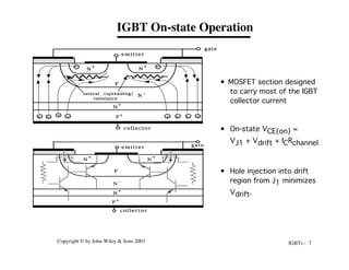
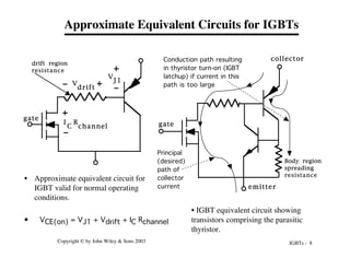
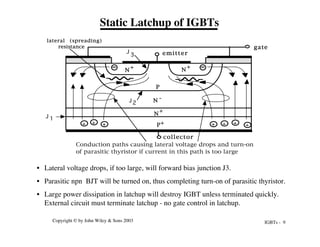
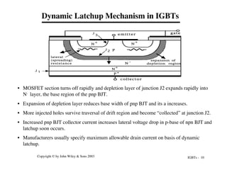
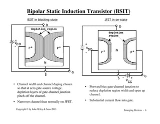
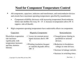
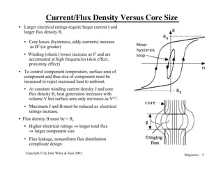
The document provides an overview of power electronic systems, covering topics such as linear and switch-mode power supplies, power semiconductor switches, and basic electrical and magnetic circuit concepts. It discusses applications of power electronics in driving adjustable speed motors, the characteristics of various semiconductor devices like diodes, thyristors, and MOSFETs, as well as computer simulations of power electronic converters. Various rectification methods and their implications on circuit performance, including current commutation and filtering are also addressed.


![Semiconductor Physics - 7
Copyright © by John Wiley & Sons 2003
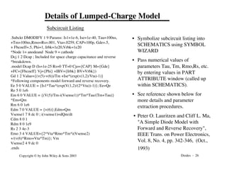
Carrier Lifetimes
• t = excess carrier lifetime
• Usually assumed to be constant. Changes in two important situations.
• t increases with temperature T
• t decreases at large excess carrier densities ; t = to/[1 + (dn/nb)2 ]
• Control of carrier lifetime values.
• Switching time-on state loss tradeoff mandates good lifetime control.
• Control via use of impurities such as gold - lifetime killers.
• Control via electron irradiation - more uniform and better control.](https://image.slidesharecdn.com/powerelectronics-convertersapplicationsanddesign-3rdedition-240423184614-112eb1ad/85/Power_Electronics_-__Converters__Applications__and_Design-_3rd_edition-pdf-445-320.jpg)
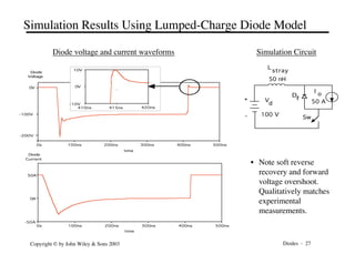
![Semiconductor Physics - 14
Copyright © by John Wiley & Sons 2003
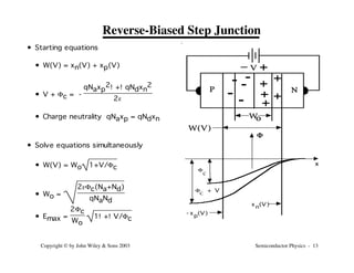
Forward-Biased PN Junction
+
+
+
P N
V
W(V)
np o
p
n o
x
Wo
pn(x) = pn(0) exp(
x
L p
)
pn(0) =
ni
2
Nd
exp(
qV
kT
)
np(0)
ni
2
Na
exp(
qV
kT
) =
Qn = Ú
0
!-!∞
!np(x)dx = q
Î
Í
Í
È
˚
˙
˙
˘
np(0)!-!
ni
2
Na
! Qp = Ú
0
!!∞
!pn(x)dx = q
Î
Í
Í
È
˚
˙
˙
˘
pn(0)!-!
ni
2
Nd
!
np(x) = np(0) exp(
x
Ln
)
-
p-side drift
region
n-side drift
region
È È
• Forward bias favors
diffusion over drift.
• Excess minority
carrier injection into
both p and n drift
regions.
• Minority carrier
diffusion lengths.
• Ln = [Dntn]0.5
• Lp = [Dptp]0.5](https://image.slidesharecdn.com/powerelectronics-convertersapplicationsanddesign-3rdedition-240423184614-112eb1ad/85/Power_Electronics_-__Converters__Applications__and_Design-_3rd_edition-pdf-452-320.jpg)
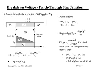
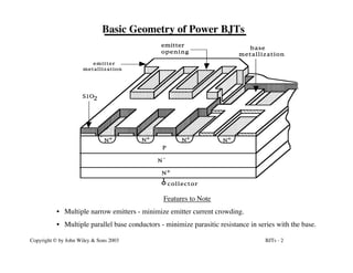
![Diodes - 3
Copyright © by John Wiley & Sons 2003
Breakdown Voltage Estimate - Step Junction
W(V)
x
F
Fc
F + V
c
• Non- punch- through diode. Drift
region length Wd >W(BVBD) =
length of space charge region at
breakdown.
• W(V) = Wo 1+V/Fc
• Wo =
2eFc(Na+Nd)
qNaNd
• Emax =
2Fc
Wo
1!+!V/Fc
• Power di ode at r ever se br eakdown:
Na >
> Nd ; E = EBD ; V = BVBD >
> Fc
• W2(BVBD) =
Wo
2!BVBD
Fc
; Wo
2 =
2eFc
q!Nd
• Concl usi ons
1. Lar ge BVBD (103 V) r equi r es Nd < 1015 cm- 3
2. Lar ge BVBD (103 V) r equi r es N- dr i ft r egi on > 100 µ m
• (Emax)2 = (EBD)2 =
4!Fc
Wo
2
BVBD
• Solve for W(BVBD) and BVBD
to obtain (put in Si values)
BVBD =
e!EBD
2
2!q!Nd
=
1.3x10¹⁷
Nd
; [V]
W(BVBD) =
2!BVBD
EBD
= 10- 5 BVBD ; [µm]](https://image.slidesharecdn.com/powerelectronics-convertersapplicationsanddesign-3rdedition-240423184614-112eb1ad/85/Power_Electronics_-__Converters__Applications__and_Design-_3rd_edition-pdf-458-320.jpg)

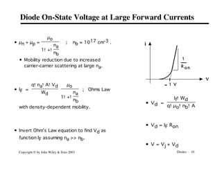
![Diodes - 9
Copyright © by John Wiley & Sons 2003
Drift Region On-State Voltage Estimate
• IF =
QF
t
=
q!A!Wd!na
t
; Current needed
to maintain stored charge QF.
• IF =
q![µn!+!µp]!na!A!Vd
Wd
;
Ohm’s Law (J = sE)
• Vd =
Wd
2
![µn!+!µp]!t
; Equate above
two equations and solve for Vd
• Conclusion: long lifetime t minimizes Vd.
P
+
N+
x
-
+
N
-
W
d
I F
+ -
V
d
Cross-sectional
area = A
V
j
+ -](https://image.slidesharecdn.com/powerelectronics-convertersapplicationsanddesign-3rdedition-240423184614-112eb1ad/85/Power_Electronics_-__Converters__Applications__and_Design-_3rd_edition-pdf-464-320.jpg)
![Diodes - 15
Copyright © by John Wiley & Sons 2003
Carrier Lifetime-Breakdown Voltage Tradeoffs
• Low on-state losses require
L = D!t =
kT
q![µn!+!µp]
!t
L = Wd ≥ W(V) = 10-5BVBD
• Solving for the lifetime yields
t =
Wd
2
(kT/q)![µn+µp]
= 4x10-12 (BVBD)2
• Substituting for t in Irr and trr equations gives
• trr = 2.8x10⁻⁶ BVBD
IF
(diR/dt)
• Irr = 2.8x10⁻⁶ BVBD IF!
diR
dt
Conclusions
1. Higher breakdown voltages
require larger lifetimes if low
on-state losses are to be
maintained.
2. High breakdown voltage
devices slower than low
breakdown voltage
devices.
3. Turn-off times shortened
by large
diR
dt
but Irr is
increased.](https://image.slidesharecdn.com/powerelectronics-convertersapplicationsanddesign-3rdedition-240423184614-112eb1ad/85/Power_Electronics_-__Converters__Applications__and_Design-_3rd_edition-pdf-470-320.jpg)
![Diodes - 21
Copyright © by John Wiley & Sons 2003
PN Vs Schottkys at Large BVBD
• Minority carrier drift region
relationships
• IF ≈
q"[µn"+"µp]"na"A"Vd
Wd
• Maximum practical value of na =1017
cm-3 and corresponding to
µn + µp = 900 cm2/(V-sec)
• Desired breakdown voltage requires
Wd ≥ 10-5 BVBD
IF
A
= 1.4x10⁶ Vd
BVBD
• Majority carrier drift region
relationships
• IF ≈
q"[µn"+"µp]"Nd"A"Vd
Wd
• Desired breakdown voltage
requires Nd =
1.3x10¹⁷
BVBD
and
Wd ≥ 10-5 BVBD
• Large BVBD (1000 V) requires Nd
= 1014 cm-3 where µn + µp =
1500 cm2/(V-sec)
•
IF
A
≈ 3.1x10⁶
Vd
[BVBD]2
• Conclusion: Minority carrier
devices have lower on-state
losses at large BVBD.](https://image.slidesharecdn.com/powerelectronics-convertersapplicationsanddesign-3rdedition-240423184614-112eb1ad/85/Power_Electronics_-__Converters__Applications__and_Design-_3rd_edition-pdf-476-320.jpg)


![MOSFETs - 5
Copyright © by John Wiley & Sons 2003
MOSFET I-V Characteristics and Circuit Symbols
G
S
D
S
G
D
N-channel
MOSFET
P-channel
MOSFET
i
D
v
GS
V
GS(th)
actual
linearized
a c t i v e
o h m i c
i
D
v
D S
B V
D S S
VG S 1
G S 2
V
G S 3
V
G S 4
V
G S 5
V
[v - V = v ]
G S GS(th) D S
V
GS(th)
V <
G S](https://image.slidesharecdn.com/powerelectronics-convertersapplicationsanddesign-3rdedition-240423184614-112eb1ad/85/Power_Electronics_-__Converters__Applications__and_Design-_3rd_edition-pdf-514-320.jpg)
![MOSFETs - 15
Copyright © by John Wiley & Sons 2003
Turn-on Gate Charge Characteristic
Qon = ı
Û
Vgs,off
(Vt+ID1/gm)
![Cgs(Vgs)!+!Cgd(Vgs)]!Vgs!dVgs
Qp = ı
Û
Vd
Vds,on
!Cgd(Vds)!Vds
!dVds
QT = Qon + Qp + ı
Û
(Vt+ID1/gm)
Vgs,on
![Cgs(Vgs)!+!Cgd(Vgs)]!Vgs!dVgs
V
d
I
D1
Vgs V
ds
+
-
+
-
C
gs
C
ds
Cgd
g (V - V )
m gs t
I
D1
V
d
Vgs,off
gs,on
V
Vgs
V
t
V + I /g
m
t D1
t
t
t
V
ds,on
I
d
V
ds
Q
on
V
gs
Vgs,on
Q
p
Q
T1
Qgate
Specified I
D1
V
t
I
g
mo
+
D1
d1
V
d3
V
V
d2](https://image.slidesharecdn.com/powerelectronics-convertersapplicationsanddesign-3rdedition-240423184614-112eb1ad/85/Power_Electronics_-__Converters__Applications__and_Design-_3rd_edition-pdf-524-320.jpg)
![MOSFETs - 19
Copyright © by John Wiley & Sons 2003
• VGS(max) = maximum per missible gate-
sour ce voltage.
• If VGS >VGS(max) r uptur e of gate oxide by
lar ge electr ic fields possible.
• EBD(oxide) ≈ 5- 10 million V/cm
• Gate oxide typically 1000 anstr oms thick
• VGS(max) < [5x10⁶] [10- 5] = 50 V
• Typical VGS(max) 20 - 30 V
• Static char ge on gate conductor can r uptur e
gate oxide
• Handle MOSFETs with car e (gr ound
your self befor e handling device)
• Place anti- par allel connected Zener diodes
between gate and sour ce as a pr otective
measur e
Maximum Gate-Source Voltage](https://image.slidesharecdn.com/powerelectronics-convertersapplicationsanddesign-3rdedition-240423184614-112eb1ad/85/Power_Electronics_-__Converters__Applications__and_Design-_3rd_edition-pdf-528-320.jpg)
![MOSFETs - 27
Copyright © by John Wiley & Sons 2003
COOLMOS™ Operation in ON-State
• On-state specific resistance ARon [Ω-cm2]
much less than comparable VDMOS
because of higher drift region doping.
• COOLMOS™ conduction losses much
less than comparable VDMOS.
• Ron A = W/(q µnNd) ; Recall that Nd = (e EBD)/(q b)
• Breakdown voltage requirements set W = BVBD/ EBD.
• Substituting for W and Nd yields Ron A = (b BVBD)/(e µn EBD
2)
N+
N+
N+
N+
N+
source
drain
gate
cond
uctor
P
N
+
-
V1
R
L
ID
Ro n P
b
P
b
P](https://image.slidesharecdn.com/powerelectronics-convertersapplicationsanddesign-3rdedition-240423184614-112eb1ad/85/Power_Electronics_-__Converters__Applications__and_Design-_3rd_edition-pdf-536-320.jpg)
![MOSFETs - 28
Copyright © by John Wiley & Sons 2003
Ron A Comparison: VDMOS versus COOLMOS™
• COOLMOS at BVBD = 1000 V. Assume b ≈ 10 µm. Use EBD = 300 kV/cm.
• Ron A = (10-3 cm) (1000 V)/[ (9x10-14 F/cm)(12)(1500 cm2 -V-sec)(300 kV/cm)2]
Ron A = 0.014 Ω-cm . Corresponds to Nd = 4x1015 cm-3
• Typical VDMOS, Ron A = 3x10⁻⁷ (BVBD)2
• Ron A = 3x10⁻⁷ (1000)2 = 0.3 Ω-cm ; Corresponding Nd= 1014 cm3
• Ratio COOLMOS to VDMOS specific resistance = 0.007/0.3 = 0.023 or approximately 1/40
• At BVBD = 600 V, ratio = 1/26.
• Experimentally at BVBD = 600 V, ratio is 1/5.
• For more complete analysis see: Antonio G.M. Strollo and Ettore Napoli, “Optimal ON-Resistance
Versus Breakdown Voltage Tradeoff in Superjunction Power Device: A Novel Analytical Model”, IEEE
Trans. On Electron Devices,Vol. 48, No. 9, pp 2161-2167, (Sept., 2001)](https://image.slidesharecdn.com/powerelectronics-convertersapplicationsanddesign-3rdedition-240423184614-112eb1ad/85/Power_Electronics_-__Converters__Applications__and_Design-_3rd_edition-pdf-537-320.jpg)

![MOSFETs - 33
Copyright © by John Wiley & Sons 2003
10V 20V 30V
0V
0
2
4
[nF]
SPICE model
Motorola subcircuit model
Cgd
V
DS
V = 0
GS
MTP3055E
100ns 200ns 300ns
Time
40V
20V
60V
0V
0s
V
DS
SPICE
model
Motorola
subcircuit
model
MTP3055E
• Cgs and Cgd in PSPICE model are
constant independent of terminal voltages
• In vertical power MOSFETs, Cgd varies
substantially with terminal voltages.
• Comparison of transient response of drain-
source voltage using PSPICE model and
an improved subcircuit model. Both
models used in same step-down converter
circuit.
Inadequacies of PSPICE MOSFET Model](https://image.slidesharecdn.com/powerelectronics-convertersapplicationsanddesign-3rdedition-240423184614-112eb1ad/85/Power_Electronics_-__Converters__Applications__and_Design-_3rd_edition-pdf-542-320.jpg)


![Emerging Devices - 39
Copyright © by John Wiley & Sons 2003
Property Si GaAs 3C-SiC 6H-SiC Diamond
Bandgap @ 300 °K [ev ] 1.12 1.43 2.2 2.9 5.5
Relative dielectric
constant
11.8 12.8 9.7 10 5.5
Saturated drift
velocity [cm/sec]
1x10⁷ 2x10⁷ 2.5x10⁷ 2.5x10⁷ 2.7x10⁷
Thermal conductivity
[Watts/cm-°C]
1.5 0.5 5.0 5.0 20
Maximum operating
temperature [°K]
300 460 873 1240 1100
Intrinsic carrier
density [cm-3] @ 25 °C
1010 107 - - -
Melting temperature [°C] 1415 1238 Sublime
>1800
Sublime
>1800
Phase
change
Electron mobility
@ 300 °K [cm2/V-sec]
1400 8500 1000 600 2200
Breakdown electric
field [V/cm]
2-3x10⁵ 4x10⁵ 2x10⁶ 2x10⁶ 1x10⁷
Properties of Important Semiconductor Materials](https://image.slidesharecdn.com/powerelectronics-convertersapplicationsanddesign-3rdedition-240423184614-112eb1ad/85/Power_Electronics_-__Converters__Applications__and_Design-_3rd_edition-pdf-621-320.jpg)
![Emerging Devices - 41
Copyright © by John Wiley & Sons 2003
• Approximate design formulas for doping density and drift region length of HV pn
junctions
• Based on step junction P+N-N+ structure
• Nd = drift region doping level ≈
e"[EBD]2
2"q"BVBD
• Wd = drift region length ≈
2"BVBD
EBD
• Numerical comparison - 1000 V breakdown rating
Material Nd Wd
Si 1.3x1014 cm-3 67 µm
GaAs 5.7x10¹⁴ 50
SiC 1.1x10¹⁶ 10
Diamond 1.5x10¹⁷ 2
Material Comparison: PN Junction Diode Parameters](https://image.slidesharecdn.com/powerelectronics-convertersapplicationsanddesign-3rdedition-240423184614-112eb1ad/85/Power_Electronics_-__Converters__Applications__and_Design-_3rd_edition-pdf-623-320.jpg)
![Emerging Devices - 42
Copyright © by John Wiley & Sons 2003
• Drift region carrier lifetime required for 1000 V pn junction diode
• Approximate design formula based on step junction
t ≈
q"Wd
2
k"T"mn
=
4"q"[BVBD]2
k"T"mn"[EBD]2
• Numerical comparison
Material Lifetime
Si 1.2 µsec
GaAs 0.11 µsec
SiC 40 nsec
Diamond 7 nsec
• Shorter carrier lifetimes mean faster switching minority carrier
devices such as BJTs, pn junction diodes, IGBTs, etc.
Material Comparison: Carrier Lifetime Requirements](https://image.slidesharecdn.com/powerelectronics-convertersapplicationsanddesign-3rdedition-240423184614-112eb1ad/85/Power_Electronics_-__Converters__Applications__and_Design-_3rd_edition-pdf-624-320.jpg)


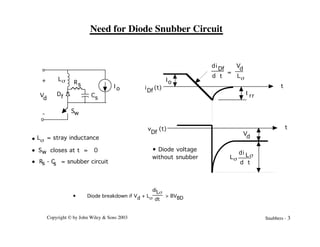
![Copyright © by John Wiley & Sons 2003 Snubbers - 6
Effect of Adding Snubber Resistance
Snubber Equivalent Circuit
Vdf
Vd
(t) = - 1 -
e-at
h!cos(f)
sin(wat - f + z) ; Rs ≤ 2 Rb
wa = wo 1-!(a/!wo)2 ; a =
Rs
2!Ls
; wo =
1
LsCs
; f = tan-1
Î
Í
Í
È
˚
˙
˙
˘
(2-x) h
4!-!hx2
h =
Cs
Cb
; x =
Rs
Rb
; Rb =
Vd
Irr
; Cb =
Ls![Irr]2
Vd
2 ; z = tan-1(a/wa)
• Governing equation Ls
d2i
dt2
+ Rs
di
dt
+
i
Cs
= 0
• Boundary conditions
i(0+) = Irr and
di(0+)
dt
=
Vd!-!IrrRs
Ls
-
V
d
Cs
R s
Ls
+
+
-
v (t)
Df
i(t)
Diode voltage as a function of time](https://image.slidesharecdn.com/powerelectronics-convertersapplicationsanddesign-3rdedition-240423184614-112eb1ad/85/Power_Electronics_-__Converters__Applications__and_Design-_3rd_edition-pdf-632-320.jpg)
![Copyright © by John Wiley & Sons 2003 Snubbers - 16
Operation of Overvoltage Snubber
vCov(0+) = Vd
• Equivalent circuit while
inductor current decays to zero
+
-
Vd
L
s
C
ov
i
Ls
+
-
iLs(0+) = Io
0
p! Ls!Cov
4
i
Ls
v
s
w
v
Cov
I
o V
d
Charge-up of C ov from Ls
Cov!(DVsw,max )2
2
=
Ls!(Io)2
2
DVsw,max
• Energy transfer from L s to Cov
Discharge of Cov thru Rov
with time constant R C
ov
ov
i
Ls
(t) = I cos[ ]
! Ls!Cov
t
o
+
-
V
d
L
s
R
ov
C
ov
Dov
i
Ls
v
Cov
+
-
• Dov on for 0 < t <
π LsCov
2
• tfi <<
π LsCov
2
• Dov,Cov provide alternate path
for inductor current as Sw turns
off.
• Switch current can fall to zero
much faster than Ls current.
• Df forced to be on
(approximating a short ckt) by Io
after Swis off.
• Equivalent circuit after turn-off
of Sw.](https://image.slidesharecdn.com/powerelectronics-convertersapplicationsanddesign-3rdedition-240423184614-112eb1ad/85/Power_Electronics_-__Converters__Applications__and_Design-_3rd_edition-pdf-642-320.jpg)

![Copyright © by John Wiley & Sons 2003 Snubbers - 21
Turn-on Snubber Design Trade-offs
Selection of inductor
• Larger Ls decreases energy dissipation in switch at turn-on
• Wsw = WB (1 + Irr/Io)2 [1 - Ls/Ls1]
• WB = VdIotfi/2 and Ls1 = Vdtfi/Io
• Ls > Ls1 Wsw = 0
• Larger Ls increases energy dissipation in RLs
• WR = WB Ls / Ls1
• Ls > Ls1 reduces magnitude of reverse recovery current Irr
• Inductor must carry current Io when switch is on - makes
inductor expensive and hence turn-on snubber seldom used
Selection of resistor RLs
• Smaller values of RLs reduce switch overvoltage Io RLs at turn-off
• Limiting overvoltage to 0.1Vd yields RLs = 0.1 Vd/Io
• Larger values of RLs shortens minimum switch off-time of 2.3 Ls/RLs](https://image.slidesharecdn.com/powerelectronics-convertersapplicationsanddesign-3rdedition-240423184614-112eb1ad/85/Power_Electronics_-__Converters__Applications__and_Design-_3rd_edition-pdf-647-320.jpg)

![Heat Sinks - 4
Copyright © by John Wiley & Sons 2003
Heat Conduction Thermal Resistance
• Generic geometry
of heat flow via
conduction
Pcond
Temperature = T
1
Temperature = T2
d
h
b
T > T
1
2
heat flow
direction
• Heat flow Pcond [W/m2] = l A (T2 - T1) / d = (T2 - T1) / Rqcond
• Thermal resistance Rqcond = d / [l A]
• Cross-sectional area A = hb
• l = Thermal conductivity has units of W-m-1-°C-1 (lAl = 220 W-m-1-°C-1 ).
• Units of thermal resistance are °C/W](https://image.slidesharecdn.com/powerelectronics-convertersapplicationsanddesign-3rdedition-240423184614-112eb1ad/85/Power_Electronics_-__Converters__Applications__and_Design-_3rd_edition-pdf-680-320.jpg)
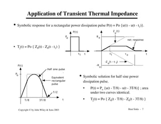
![Heat Sinks - 6
Copyright © by John Wiley & Sons 2003
Transient Thermal Impedance
• Heat capacity per unit volume Cv = dQ/dT [Joules /°C] prevents short duration high
power dissipation surges from raising component temperature beyond operating limits.
• Transient thermal equivalent
circuit. Cs = CvV where V is the
volume of the component.
P(t)
q
R
j
T (t)
a
T
Cs
P(t)
t
q
R
P
o
q
t t
Slope = 0.5
log Z (t)
q
• Transient thermal impedance Zq(t) = [Tj(t) - Ta]/P(t)
• tq = π Rq Cs /4 = thermal time
constant
• Tj(t = tq) = 0.833 Po Rq](https://image.slidesharecdn.com/powerelectronics-convertersapplicationsanddesign-3rdedition-240423184614-112eb1ad/85/Power_Electronics_-__Converters__Applications__and_Design-_3rd_edition-pdf-682-320.jpg)
![Heat Sinks - 8
Copyright © by John Wiley & Sons 2003
Zq for Multilayer Structures
P(t)
Silicon
Copper mount
Heat sink
Tj
Cu
T
c
T
a
T
• Multilayer geometry
• Transient thermal
equivalent circuit
Tj Cu
T
c
T
a
T
C (Si)
s C (Cu)
s
C (sink)
s
P(t)
R (sink)
q
R (Cu)
q
R (Si)
q
R (Si)
q
R (Cu)
q
R (Si)
q
+
R (sink)
q
R (Cu)
q
R (Si)
q
+ +
log(t)
log[Z (t)]
q
t (Si)
q
t (sink)
q
t (Cu)
q
• Transient thermal
impedance (asymptotic)
of multilayer structure
assuming widely
separated thermal time
constants.](https://image.slidesharecdn.com/powerelectronics-convertersapplicationsanddesign-3rdedition-240423184614-112eb1ad/85/Power_Electronics_-__Converters__Applications__and_Design-_3rd_edition-pdf-684-320.jpg)

![Heat Sinks - 10
Copyright © by John Wiley & Sons 2003
Radiative Thermal Resistance
• Stefan-Boltzmann law describes radiative heat transfer.
• Prad = 5.7x10⁻⁸ EA [( Ts)4 -( Ta)4 ] ; [Prad] = [watts]
• E = emissivity; black anodized aluminum E = 0.9 ; polished aluminum E = 0.05
• A = surface area [m2]through which heat radiation emerges.
• Ts = surface temperature [°K] of component. Ta = ambient temperature [°K].
• (Ts - Ta )/Prad = R q,rad = [Ts - Ta][5.7EA {( Ts/100)4 -( Ta/100)4 }]-1
• Example - black anodized cube of aluminum 10 cm on a side. Ts = 120 °C and
Ta = 20 °C
• Rq,rad = [393 - 293][(5.7) (0.9)(6x10⁻²){(393/100)4 - (293/100)4 }]-1
• Rq,rad = 2.2 °C/W](https://image.slidesharecdn.com/powerelectronics-convertersapplicationsanddesign-3rdedition-240423184614-112eb1ad/85/Power_Electronics_-__Converters__Applications__and_Design-_3rd_edition-pdf-686-320.jpg)
![Heat Sinks - 11
Copyright © by John Wiley & Sons 2003
Convective Thermal Resistance
• Pconv = convective heat loss to surrounding air from a vertical surface at sea level having
a height dvert [in meters] less than one meter.
• Pconv = 1.34 A [Ts - Ta]1.25 dvert
-0.25
• A = total surface area in [m2]
• Ts = surface temperature [°K] of component. Ta = ambient temperature [°K].
• [Ts - Ta ]/Pconv = Rq,conv = [Ts - Ta ] [dvert]0.25[1.34 A (Ts - Ta )1.25]-1
• Rq,conv = [dvert]0.25 {1.34 A [Ts - Ta]0.25}-1
• Example - black anodized cube of aluminum 10 cm on a side. Ts = 120 °C and Ta = 20 °C.
• Rq,conv = [10-1]0.25([1.34] [6x10⁻²] [120 - 20]0.25)-1
• Rq,conv = 2.2 °C/W](https://image.slidesharecdn.com/powerelectronics-convertersapplicationsanddesign-3rdedition-240423184614-112eb1ad/85/Power_Electronics_-__Converters__Applications__and_Design-_3rd_edition-pdf-687-320.jpg)
![Heat Sinks - 12
Copyright © by John Wiley & Sons 2003
Combined Effects of Convection and Radiation
• Heat loss via convection and radiation occur in parallel.
• Steady-state thermal equivalent circuit
• Rq,sink = Rq,rad Rq,conv / [Rq,rad + Rq,conv]
• Example - black anodized aluminum cube 10 cm per side
• Rq,rad = 2.2 °C/W and Rq,conv = 2.2 °C/W
• Rq,sink = (2.2) (2.2) /(2.2 + 2.2) = 1.1 °C/W
P R
q,conv
q,rad
R
s
T
a
T](https://image.slidesharecdn.com/powerelectronics-convertersapplicationsanddesign-3rdedition-240423184614-112eb1ad/85/Power_Electronics_-__Converters__Applications__and_Design-_3rd_edition-pdf-688-320.jpg)


![Magnetics - 11
Copyright © by John Wiley & Sons 2003
Quantitative Description of Core Losses
• Eddy current loss plus hysteresis loss =
core loss.
• Empirical equation - Pm,sp = k fa [Bac]
d
.
f = frequency of applied field. Bac =
base-to-peak value of applied ac field. k,
a, and d are constants which vary from
material to material
• Pm,sp = 1.5x10⁻⁶ f1.3 [Bac]
2.5
mW/cm3 for 3F3 ferrite. (f in kHz and
B in mT)
• Pm,sp = 3.2x10⁻⁶ f1.8 [Bac]2
mW/cm3 METGLAS 2705M (f in kHz
and B in mT)
• Example: 3F3 ferrite with f = 100 kHz
and Bac = 100 mT, Pm,sp = 60
mW/cm3
• 3F3 core losses in graphical form.](https://image.slidesharecdn.com/powerelectronics-convertersapplicationsanddesign-3rdedition-240423184614-112eb1ad/85/Power_Electronics_-__Converters__Applications__and_Design-_3rd_edition-pdf-699-320.jpg)
![Magnetics - 15
Copyright © by John Wiley & Sons 2003
Eddy Current Losses in Laminated Cores
x
dx
-x
L
d
w
B sin( wt)
x
y
z
Eddy current flow path
• Flux f(t) intercepted by current loop
of area 2xw given by f(t) = 2xwB(t)
• Voltage in current loop v(t) = 2xw
dB(t)
dt
= 2wxwBcos(wt)
• Current loop resistance r =
2wrcore
L!dx
; w >> d
• Instantaneous power dissipated in thin loop
dp(t) =
[v(t)]2
r
• Average power Pec dissipated in lamination
given by Pec = <ı
Ûdp(t)dV > =
w!L!d3!w2!B2
24!rcore
• Pec,sp =
Pec
V
=
w!L!d3!w2!B2
24!rcore
1
dwL
=
d2!w2!B2
24!rcore
• Average power Pec dissipated in lamination
given by Pec = <ı
Ûdp(t)dV > =
w!L!d3!w2!B2
24!rcore
• Pec,sp =
Pec
V
=
w!L!d3!w2!B2
24!rcore
1
dwL
=
d2!w2!B2
24!rcore](https://image.slidesharecdn.com/powerelectronics-convertersapplicationsanddesign-3rdedition-240423184614-112eb1ad/85/Power_Electronics_-__Converters__Applications__and_Design-_3rd_edition-pdf-703-320.jpg)
![Magnetics - 19
Copyright © by John Wiley & Sons 2003
R
ec
R
dc
d = conductor
diameter or
thickness
Resistance
d ≈ d
opt
Minimum Winding Loss
• Pw = Pdc + Pec ; Pec = eddy current loss.
• Pw = { Rdc + Rec} [Irms]2 = Rac [Irms]2
• Rac = FR Rdc = [1 + Rec/Rdc] Rdc
Optimum conductor size
• Minimum winding loss at optimum conductor size.
• Pw = 1.5 Pdc
• Pec = 0.5 Pdc
• High frequencies require small conductor sizes minimize loss.
• Pdc kept small by putting may small-size conductors in parallel using
Litz wire or thin but wide foil conductors.](https://image.slidesharecdn.com/powerelectronics-convertersapplicationsanddesign-3rdedition-240423184614-112eb1ad/85/Power_Electronics_-__Converters__Applications__and_Design-_3rd_edition-pdf-707-320.jpg)

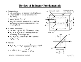
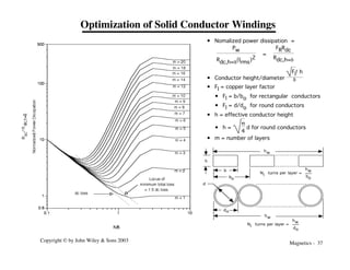
![Magnetics - 21
Copyright © by John Wiley & Sons 2003
Scaling of Core Flux Density and Winding Current Density
• Power per unit volume, Psp, dissipated in magnetic
component is Psp = k1/a ; k1 = constant and
a = core scaling dimension.
• Pw,sp Vw + Pm,sp Vm =
Ts!-!Ta
Rqsa
:
Ta = ambient temperature and Rqsa =
surface-to-ambient thermal resistance of component.
• For optimal design Pw,sp = Pc,sp = Psp :
Hence Psp =
Ts!-!Ta
Rqsa(Vw!+!Vc)
• Rqsa proportional to a2 and (Vw + Vc)
proportional to a3
• Jrms =
Psp
kcu!rcu
= k2
1
kcua
; k2 = constant
• Pm,sp = Psp = k fb [Bac]d ; Hence
Bac =
d Psp
kfb =
k3
d
fb!a
where k3 = constant
• Plots of Jrms , Bac , and Psp versus core size
(scale factor a) for a specific core material, geometry,
frequency, and Ts - Ta value very useful for picking
appropriate core size and winding conductor size.](https://image.slidesharecdn.com/powerelectronics-convertersapplicationsanddesign-3rdedition-240423184614-112eb1ad/85/Power_Electronics_-__Converters__Applications__and_Design-_3rd_edition-pdf-709-320.jpg)
![Magnetics - 22
Copyright © by John Wiley & Sons 2003
0
1
2
3
4
5
6
7
8
0
50
100
150
200
250
300
350
400
0.5 1 1.5 2 2.5 3 3.5 4 4.5 5
mW/cm 3
A/mm 2
Core scaling parameter a [cm]
P
s p
J rms P
s p
J rms
Example of Power Density and Current Density Scaling
Assumptions
1. Double-E core made from 3F3 ferrite
2. Ts = 100 °C and Ta = 40 °C.
3. Winding made with Leitz wire - kcu =
0.3](https://image.slidesharecdn.com/powerelectronics-convertersapplicationsanddesign-3rdedition-240423184614-112eb1ad/85/Power_Electronics_-__Converters__Applications__and_Design-_3rd_edition-pdf-710-320.jpg)
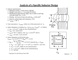
![Magnetics - 24
Copyright © by John Wiley & Sons 2003
Analysis of a Specific Inductor Design (cont.)
• L =
N!f
I
= 310 mH
• f = Bac Ac = (0.18 T)(1.5x10⁻⁴ m2) = 2.6x10⁻⁵ Wb
• Surface temperature Ts = Ta + Rqsa (Pw + Pcore) = 104 °C
• Rqsa = Rq,rad || Rq,conv = 9.8 °C/W
• Rq,rad =
60
(5.1)!(0.006)!Ë
Á
Ê
¯
˜
ˆ
Ë
Á
Ê
¯
˜
ˆ
373
100
4
!-!Ë
Á
Ê
¯
˜
ˆ
313
100
4
! !
= 20.1 [°C/W]
• Rq,conv =
1
(1.34)(0.006)
4
0.035
60
= 19.3 [°C/W]
• Overcurrent of 25% (I= 5 amp rms) makes Ts = 146 °C
• Pw = (3.2 W)(1.25)2 = 5 W ; Pcore = (3.3 W)(1.25)2.5 = 5.8 W
• Ts = (9.8 °C/W)(10.8 W) + 40 °C = 146 °C
fringing
flux
g
g
A core
A g
g
a
d](https://image.slidesharecdn.com/powerelectronics-convertersapplicationsanddesign-3rdedition-240423184614-112eb1ad/85/Power_Electronics_-__Converters__Applications__and_Design-_3rd_edition-pdf-712-320.jpg)
![Magnetics - 25
Copyright © by John Wiley & Sons 2003
Stored Energy Relation - Basis of Inductor Design
• Design consists of the following:
• Selection of core geometric shape and size
• Core material
• Winding conductor geometric shape and size
• Number of turns in winding
• Input specifications for inductor design
• Inductance value L.
• Rated peak current I
• Rated rms current Irms.
• Rated dc current (if any) Idc.
• Operating frequency f.
• Maximum inductor surface temperature Ts
and maximum ambient temperature Ta.
Goal: Minimize inductor size, weight, and cost.
• Design procedure starting point - stored energy relation
• [L I] Irms = [N f] Irms
• N =
kcu!Aw
Acu
• f = B Acore ; Irms = Jrms Acu
• L I Irms = kcu Jrms B Aw Acore
• Equation relates input specifications (left-hand side) to
needed core and winding parameters (right-hand side)
• A good design procedure will consists of a systematic,
single-pass method of selecting kcu, Jrms, B, Aw, and Acore.](https://image.slidesharecdn.com/powerelectronics-convertersapplicationsanddesign-3rdedition-240423184614-112eb1ad/85/Power_Electronics_-__Converters__Applications__and_Design-_3rd_edition-pdf-713-320.jpg)

![Magnetics - 27
Copyright © by John Wiley & Sons 2003
Details of Interactive Inductor Core Database Calculations
• User inputs: L, I, Irms, Idc, f, Ts, Ta, and kcu
• Stored information (static, independent of converter requirements)
• Core dimensions, Aw, Acore, Vc, Vw, surface area, mean turn length, mean magnetic path length, etc.
• Quantitative core loss formulas for all materials of interest including approximate temperature dependence.
• Calculation of core capabilities (stored energy value)
1. Compute converter-required stored energy value: L I Irms.
2. Compute allowable specific power dissipation Psp = [Ts - Ta] /{ Rqsa [Vc + Vw ]}. Rqsa = h/As or calculated
interactively using input temperatures and formulas for convective and radiative heat transfer from Heat Sink
chapter.
3. Compute allowable flux density Psp = k fb [Bac]d and current density Psp = kcu rcu {Jrms}2.
4. Compute core capabilities kcu Aw Acore B Jrms
• Calculation of inductor design parameters.
1. Area of winding conductor Acu = I / Jrms.
2. Calculate skin depth d in winding. If Acu > d2at the operating frequency, then single round conductor cannot
be used for winding.
• Construct winding using Leitz wire, thin foils, or paralleled small dia. (≤ d) round wires.](https://image.slidesharecdn.com/powerelectronics-convertersapplicationsanddesign-3rdedition-240423184614-112eb1ad/85/Power_Electronics_-__Converters__Applications__and_Design-_3rd_edition-pdf-715-320.jpg)


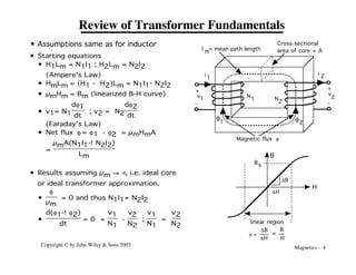
![Magnetics - 38
Copyright © by John Wiley & Sons 2003
x
x
x
x x x
x x
x
x
x
x
0 bw
x
MMF
Npri Ipri = Nsec I sec
x Primary
Secondary
hw
Direction and relative
magnitude of leakage
magnetic field.
x = current
into page
• = current
out of page
Transformer Leakage Inductance
• Linear variation of mmf in winding window indicates
spatial variation of magnetic flux in the window and thus
incomplete flux linkage of primary and secondary windings.
• Hwindow = Hleak =
2!Npri!Ipri!x
hw!bw
; 0 < x < bw/2
Hleak =
2!Npri!Ipri
hw
(1 - x/bw) ; bw/2 < x < bw
•
Lleak!(Ipri)2
2
=
1
2
ı
Ù
Û
Vw
mo(Hleak)2dV
• Volume element dV = hw lw(x)dx ; lw(x) equals the
length of the conductor turn located at position x.
• Assume a mean turn length lw ≈ 8a for double-E
core independent of x.
•
Lleak!(Ipri)2
2
= (2)
1
2 ı
Ù
Ù
Û
0
bw/2
mo[
2!Npri!Ipri!x
hw!bw
]2!hw!lwdx
• Lleak =
mo!(Npri)2!lw!bw
3!p2!!hw
• If winding is split into p+1 sections, with p > 1,
leakage inductance is greatly reduced.
• Transformer leakage inductance causes
overvoltages across power switches at turn-off.
• Leakage inductance caused by magnetic
flux which does not completely link primary
and secondary windings.](https://image.slidesharecdn.com/powerelectronics-convertersapplicationsanddesign-3rdedition-240423184614-112eb1ad/85/Power_Electronics_-__Converters__Applications__and_Design-_3rd_edition-pdf-726-320.jpg)

![Magnetics - 40
Copyright © by John Wiley & Sons 2003
Core Database - Basic Transformer Design Tool
• Interactive core database (spreadsheet-based) key to a single pass tramsformer design procedure.
• User enters input specifications from converter design requirements. Type of conductor for windings
(round wire, Leitz wire, or rectangular wire or foil) must be made so that copper fill factor kcu is known.
• Spreadsheet calculates capability of all cores in database and displays smallest size core of each type
that meets V- I specification.
• Also can be designed to calculate (and display as desired) design output parameters including Jrms, B,
Acu,pri, Acu,sec, Npri, Nsec, and leakage inductance..
• Multiple iterations of core material and winding conductor choices can be quickly done to aid in
selection of most appropriate tranformer design.
• Information on all core types, sizes, and materials must be stored on spreadsheet. Info includes
dimensions, Aw, Acore, surface area of assembled transformer , and loss data for all materials of interest.
• Pre-stored information combined with user inputs to produce performance data for each core in
spreadsheet. Sample of partial output shown below.
Core
No.
Material AP =
AwAc
Rq
DT=60 °C
Psp @
Ts=100 °C
Jrms @
Ts=100 °C
& Psp
B
^
rated @
Ts=100 °C
& 100 kHz
2.22 kcu f Jrms B
^ AP
(f = 100kHz)
• • • • • • • •
8 3F3 2.1
cm
4
9.8 °C/W 237
mW/cm
3
(3.3/ kcu
)
•
Rdc
Rac
A/mm2
170 mT 2.6x10³ •
kcuRdc
Rac
[V-A]
• • • • • • • •](https://image.slidesharecdn.com/powerelectronics-convertersapplicationsanddesign-3rdedition-240423184614-112eb1ad/85/Power_Electronics_-__Converters__Applications__and_Design-_3rd_edition-pdf-728-320.jpg)
![Magnetics - 41
Copyright © by John Wiley & Sons 2003
Details of Interactive Transformer Core Database Calculations
• User inputs: Vpri, Ipri, turns ratio Ndc/ Nsec, f, Ts, Ta, and kcu
• Stored information (static, independent of converter requirements)
• Core dimensions, Aw, Acore, Vc, Vw, surface area, mean turn length, mean magnetic path length, etc.
• Quantitative core loss formulas for all materials of interest including approximate temperature dependence.
• Calculation of core capabilities
1. Compute converter-required stored energy value: S = 2 Vpri Ipri
2. Compute allowable specific power dissipation Psp = [Ts - Ta] /{ Rqsa [Vc + Vw ]}. Rqsa = h/As or calculated
interactively using input temperatures and formulas for convective and radiative heat transfer from Heat Sink
chapter.
3. Compute allowable flux density Psp = k fb [Bac]d and current density Psp = kcu rcu {Jrms}2.
4. Compute core capabilities 4.4 f kcu Aw Acore Bac Jrms
• Calculation transformer parameters.
1. Calculate number of primary turns Npri = Vpri /{2π f AcpreBac} and secondary turns Nsec = Vsec /{2π f AcpreBac}
2. Calculate winding conductor areas assuming low frequencies or use of Leitz wire
• Acu,pri = [kcuAw]/[2 Npri] and Acu,sec = [kcuAw]/[2 Nsec]](https://image.slidesharecdn.com/powerelectronics-convertersapplicationsanddesign-3rdedition-240423184614-112eb1ad/85/Power_Electronics_-__Converters__Applications__and_Design-_3rd_edition-pdf-729-320.jpg)
![Magnetics - 42
Copyright © by John Wiley & Sons 2003
Details of Interactive Transformer Core Database Calculations (cont.)
3. Calculate winding areas assuming eddy current/proximity effect is important
• Only solid conductors, round wires or rectangular wires (foils), used.Jrms = [{Psp Rdc}/{Rac kcu rcu}]1/2
• Conductor dimensions must simultaneously satisfy area requirements and requirements of normalized
power dissipation versus normalized conductor dimensions.
• May require change in choice of conductor shape. Most likely will require choice of foils (rectangular
shapes).
• Several iterations may be needed to find proper combinations of dimensions, number of turns per layer,
and number of layers and sections.
• Best illustrated by a specific design example.
4. Estimate leakage inductance Lleak= {µo{Npri}2 lw bw}/ {3 p2 hw}
5. Estimate Smax = 4.4 kcu f Acore Aw Jrms Bac
6. If Smax > S = 2 Vpri Ipri reduce Smax and save on copper cost, weight, and volume.
• If Npri w Ac Bac > Vpri, reduce Smax by reducing Npri and Nsec.
• If Jrms Acu, pri > Irms, reduce Acu,pri and Acu, sec.
• If S > Smax by only a moderate amount (10-20%) and smaller than Smax of next core size, increase Smax of
present core size.
• Increase Irms (and thus winding power dissipation) as needed.Temperature Ts will increase a modest amount
above design limit, but may be preferable to going to larger core size.](https://image.slidesharecdn.com/powerelectronics-convertersapplicationsanddesign-3rdedition-240423184614-112eb1ad/85/Power_Electronics_-__Converters__Applications__and_Design-_3rd_edition-pdf-730-320.jpg)
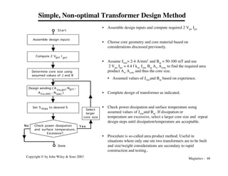


![Fundamentals of power electronics [presentation slides] 2nd ed r. erickson ww](https://cdn.slidesharecdn.com/ss_thumbnails/fundamentalsofpowerelectronicspresentationslides2nded-r-ericksonww-100522135011-phpapp02-thumbnail.jpg?width=640&height=640&fit=bounds)