This document summarizes research on the microstructure and optical properties of Cu@Ni core-shell nanoparticles embedded in a carbon-hydrogen (C:H) thin film. The nanoparticles were prepared using RF sputtering and RF PECVD deposition of copper followed by nickel layers of varying thicknesses. Atomic force microscopy showed nanoparticles ranging from 6-14 nm in size. X-ray diffraction revealed the formation of Cu and Ni nanocrystals with oxidation occurring upon air exposure. UV-VIS-NIR spectroscopy demonstrated surface plasmon resonance absorption from the Cu nanoparticles around 600 nm that was dampened by increasing nickel layer thickness, while absorbance in the near-infrared region and the edge of strong absorption varied with nickel thickness.
![ISSN 2070 2051, Protection of Metals and Physical Chemistry of Surfaces, 2015, Vol. 51, No. 4, pp. 575–578. © Pleiades Publishing, Ltd., 2015.
575
1 INTRODUCTION
Metallic nanoparticles have been the subject of
extensive research because of their potential applica
tions in many areas [1, 2] and the remarkable physics
involved in the process. In recent years, nanoparticle
based optical surface plasmon sensors have attracted
attention in the research community because of their
faster response time and better resolution [3]. Semi
conductor oxide nanoparticles are used as a base for
gas sensors; the addition of a metallic core inside this
oxide can improve the sensitivity and selectivity of the
sensor [4]. The surface of copper oxide can react with
gases or solutions and behave as a catalyst or a gas sen
sor; however, the surface properties of metal oxides are
not well understood [5]. The deposition of artificially
layered structures using multiple metals exhibiting dif
ferent mechanical or magnetic properties is important
because of their application in areas such as intercon
nects, giant magnetoresistive, sensors, and data stor
age devices [6, 7]. Cu/Ni films have potential applica
tions in magneto optical recording and spintronic [8].
EXPERIMENTAL DETAILS
The Cu@Ni core shell nanoparticles on the a C:H
thin film were prepared using a capacitance coupled
RF PECVD system with a 13.56 MHz power supply.
1 The article is published in the original.
The reactor consisted of two electrodes with different
areas. The smaller electrode was a Cu plate used as a
powered electrode in the first step of deposition and a
Ni plate in the second step of deposition. The other
electrode was grounded in the body of the stainless
steel chamber. Deposition was done at room tempera
ture on the glass and silicon substrates of the electrode.
The chamber was evacuated to a base pressure of about
10–5 mbar prior to deposition and then the pressure
was raised to the desired ambient pressure using acet
ylene gas flow.
The deposition was done in two steps (Cu and Ni
deposition). In the first step, for the growth of Cu
nanoparticles, the power was held at around 180 W,
and initial gas pressure was varied from 0.03 to 0.05
mbar. Ni of different thicknesses was grown over the
Cu nanoparticles. The deposition time for the Cu core
was 20 min and the thickness of the film was 50–100
nm. The deposition time for the Ni shells were 1, 7,
and 10 min and their thicknesses were less than 10 nm.
The thickness of the film was measured using a Tencor
Alpha step 500 profiler. The optical properties of the
samples were obtained from UV VIS near IR spectra.
AFM in the non contact mode was used to obtain the
surface topography of the film and average particle
size. Also, the root mean square (RMS) values and the
power spectral density (PSD) curves used throughout
this work were calculated from selected AFM scans
with the Nanotec off line analysis software.
Microstructure and Optical Properties
of Cu@Ni Nanoparticles Embedded in a C:H1
Ali Armana, Tayebeh Ghodselahib, Mehrdad Molamohammadic, Shahram Solaymania,
Hadi Zahrabic, and Azin Ahmadpourianc
a
Young Researchers and Elite Club, Kermanshah Branch, Islamic Azad University, Kermanshah, Iran
b
Nano Mabna Iranian Inc., Po Box 1676664116, Tehran, Iran
cDepartments of Physics, Kermanshah Branch, Islamic Azad University, Kermanshah, Iran
e mail: ali.arman173@gmail.com; ali.gelali@gmail.com
Received November 13, 2013
Abstract—Cu@Ni core shell nanoparticles on a C:H thin film were prepared by co deposition of RF sput
tering and RF PECVD. Samples having different Cu nanoparticle sizes were grown and then Ni layers of dif
ferent thicknesses were grown over these Cu nanoparticles. Atomic force microscopy indicated that the thin
film consisted of nanoparticles 6–14 nm in size. Also, in the present work the RMS roughness and PSD spec
tra computed from atomic force microscopy (AFM) data were used for studying the morphology of thin films.
X ray diffraction (XRD) profiles show that the Cu nanocrystal core and Ni nanocrystal shell have formed in
the film and that the surfaces of these core shells oxidize when exposed to air. The surface plasmon resonance
peak of the Cu nanoparticles can be observed at about 600 nm in a region damped by the increased thickness
of the Ni layer. Absorbance in the near IR region increased as the thickness of the Ni layer increased. The
edge of strong absorption observed near the IR region varied with the thickness of the Ni layer.
DOI: 10.1134/S2070205115040036
NANOSCALE AND NANOSTRUCTURED
MATERIALS AND COATINGS](https://image.slidesharecdn.com/b925ea81-08ff-46e9-bc2f-4c66824b8994-150812102758-lva1-app6892/85/PM575-1-320.jpg)
![ISSN 2070 2051, Protection of Metals and Physical Chemistry of Surfaces, 2015, Vol. 51, No. 4, pp. 575–578. © Pleiades Publishing, Ltd., 2015.
575
1 INTRODUCTION
Metallic nanoparticles have been the subject of
extensive research because of their potential applica
tions in many areas [1, 2] and the remarkable physics
involved in the process. In recent years, nanoparticle
based optical surface plasmon sensors have attracted
attention in the research community because of their
faster response time and better resolution [3]. Semi
conductor oxide nanoparticles are used as a base for
gas sensors; the addition of a metallic core inside this
oxide can improve the sensitivity and selectivity of the
sensor [4]. The surface of copper oxide can react with
gases or solutions and behave as a catalyst or a gas sen
sor; however, the surface properties of metal oxides are
not well understood [5]. The deposition of artificially
layered structures using multiple metals exhibiting dif
ferent mechanical or magnetic properties is important
because of their application in areas such as intercon
nects, giant magnetoresistive, sensors, and data stor
age devices [6, 7]. Cu/Ni films have potential applica
tions in magneto optical recording and spintronic [8].
EXPERIMENTAL DETAILS
The Cu@Ni core shell nanoparticles on the a C:H
thin film were prepared using a capacitance coupled
RF PECVD system with a 13.56 MHz power supply.
1 The article is published in the original.
The reactor consisted of two electrodes with different
areas. The smaller electrode was a Cu plate used as a
powered electrode in the first step of deposition and a
Ni plate in the second step of deposition. The other
electrode was grounded in the body of the stainless
steel chamber. Deposition was done at room tempera
ture on the glass and silicon substrates of the electrode.
The chamber was evacuated to a base pressure of about
10–5 mbar prior to deposition and then the pressure
was raised to the desired ambient pressure using acet
ylene gas flow.
The deposition was done in two steps (Cu and Ni
deposition). In the first step, for the growth of Cu
nanoparticles, the power was held at around 180 W,
and initial gas pressure was varied from 0.03 to 0.05
mbar. Ni of different thicknesses was grown over the
Cu nanoparticles. The deposition time for the Cu core
was 20 min and the thickness of the film was 50–100
nm. The deposition time for the Ni shells were 1, 7,
and 10 min and their thicknesses were less than 10 nm.
The thickness of the film was measured using a Tencor
Alpha step 500 profiler. The optical properties of the
samples were obtained from UV VIS near IR spectra.
AFM in the non contact mode was used to obtain the
surface topography of the film and average particle
size. Also, the root mean square (RMS) values and the
power spectral density (PSD) curves used throughout
this work were calculated from selected AFM scans
with the Nanotec off line analysis software.
Microstructure and Optical Properties
of Cu@Ni Nanoparticles Embedded in a C:H1
Ali Armana, Tayebeh Ghodselahib, Mehrdad Molamohammadic, Shahram Solaymania,
Hadi Zahrabic, and Azin Ahmadpourianc
a
Young Researchers and Elite Club, Kermanshah Branch, Islamic Azad University, Kermanshah, Iran
b
Nano Mabna Iranian Inc., Po Box 1676664116, Tehran, Iran
cDepartments of Physics, Kermanshah Branch, Islamic Azad University, Kermanshah, Iran
e mail: ali.arman173@gmail.com; ali.gelali@gmail.com
Received November 13, 2013
Abstract—Cu@Ni core shell nanoparticles on a C:H thin film were prepared by co deposition of RF sput
tering and RF PECVD. Samples having different Cu nanoparticle sizes were grown and then Ni layers of dif
ferent thicknesses were grown over these Cu nanoparticles. Atomic force microscopy indicated that the thin
film consisted of nanoparticles 6–14 nm in size. Also, in the present work the RMS roughness and PSD spec
tra computed from atomic force microscopy (AFM) data were used for studying the morphology of thin films.
X ray diffraction (XRD) profiles show that the Cu nanocrystal core and Ni nanocrystal shell have formed in
the film and that the surfaces of these core shells oxidize when exposed to air. The surface plasmon resonance
peak of the Cu nanoparticles can be observed at about 600 nm in a region damped by the increased thickness
of the Ni layer. Absorbance in the near IR region increased as the thickness of the Ni layer increased. The
edge of strong absorption observed near the IR region varied with the thickness of the Ni layer.
DOI: 10.1134/S2070205115040036
NANOSCALE AND NANOSTRUCTURED
MATERIALS AND COATINGS](https://image.slidesharecdn.com/b925ea81-08ff-46e9-bc2f-4c66824b8994-150812102758-lva1-app6892/75/PM575-1-2048.jpg)
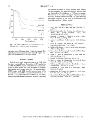
![576
PROTECTION OF METALS AND PHYSICAL CHEMISTRY OF SURFACES Vol. 51 No. 4 2015
ALI ARMAN et al.
RESULTS AND DISCUSSION
AFM images of samples 1–4 are shown in Fig. 1.
These images were used to estimate the mean size of
the nanoparticles. Figure 1e shows the abundant
topography of these samples as obtained from the
AFM data. This figure can be used to interpret the dis
tribution of particle sizes. The maximum abundance
gives the average particle size and the width provides
the variance of the particle diameter. As observed, the
average particle size of the Cu nanoparticles were 10,
10, 6, and 14 nm for samples 1, 2, 3 and 4, respectively.
The full width at the half maximum particle size distri
bution was not large for all samples.
The RMS roughness and the experimental PSD
profiles of thin films are shown in Fig. 2. Each PSD
plots was calculated using the FFT algorithm for 1 μm ×
1 μm AFM image data. It can be seen from Fig. 2h that
the PSD spectra of the thin film deposited at the Sam
ple 4 shows slower variation over the spatial frequency
[9–11]. This behavior is because of the particle size
and the amount of carbon in thin film [12]. It can be
seen that the RMS roughness values increased as the
thickness is increased Fig. 2f. It was observed that both
of the RMS roughness and PSD spectra change with
thickness and the amount of carbon in layers.
Figure 3 shows the x ray diffraction (XRD) pattern
of sample 2 on the glass and the x ray diffraction
(XRD) pattern of sample 2 with 10 min deposition
time for the Ni shell on the silicon. As shown, Cu
nanocrystals with (111), (200), and (220) orientations
Fig. 1. AFM images of samples (a) 1; (b) 2; (c) 3; (d) 4 and (e) the number of events for topography of samples 1–4.
3500
3000
2500
2000
1500
1000
500
0
5 25 30201510
(b)(а)
200 nm
(d)(c)
200 nm
200 nm200 nm
X: 1.0 µm
Y: 1.0 µm
Z: 25.5 nm
X: 1.0 µm
Y: 1.0 µm
Z: 34.3 nm
X: 1.0 µm
Y: 1.0 µm
Z: 20.1 nm
X: 1.0 µm
Y: 1.0 µm
Z: 2.1 nm
0
Abundance
Topography, nm
1
2
3
4
(e)](https://image.slidesharecdn.com/b925ea81-08ff-46e9-bc2f-4c66824b8994-150812102758-lva1-app6892/85/PM575-2-320.jpg)
![PROTECTION OF METALS AND PHYSICAL CHEMISTRY OF SURFACES Vol. 51 No. 4 2015
MICROSTRUCTURE AND OPTICAL PROPERTIES 577
and the Ni nanocrystals with (111) and (200) orienta
tions formed in the film. Traces of the Ni2O3 structure
in Fig. 2 indicate that the surface of the Cu@Ni core
shells oxidized upon exposure to air.
The UV VIS near IR absorption spectra of sam
ples 1–4, including Cu nanoparticles of different sizes,
are shown in Fig. 4. The electrical resistivity of the thin
film in samples 1 to 4 varies from several Ω to more
than 100 MΩ. In samples 3 and 2, an absorption peak
is observed at about 600 nm. This absorption peak is a
sign of the existence of Cu nanoparticles caused by
SPR [14]. An edge of strong absorption is observed for
all samples located above the SPR peak. This strong
absorption is dependent on the electrical resistivity of
the samples.
Figure 5 shows the UV VIS near IR absorption
spectra of sample 2 without the Ni layer and after 1, 7
and 10 min of Ni deposition. The SPR peak caused by
the Cu nanoparticle is damped by the increasing thick
ness of the Ni layer. The absorbance in near IR region
4.0
3.0
3.5
2.5
2.0
1.5
1.0
0.5
4.03.53.02.01.50.50 2.51.0
(f) (h)
RMS,nm
Number of Samples
–1.0
4
3
2
1
0
–1
–2
–3.0 –2.5 –2.0 –1.5
1
2
3
4
PSD[log(nm4)]
k[log({1/nm})}
Fig. 2. RMS roughness versus (f) and Power spectra density thin films (h).
40
20
80604020
0
Intensity,a.u.
2θ, deg
Intensity,a.u.
20 40 60 80
15
20
25
30
35
40
Cu(111)
Ni(111)
Cu(200)
Ni203
Si(311)
Cu(220)
Cu(111)
Cu(200)
(а) (b)
2θ, deg
Fig. 3. X ray diffraction profile pattern (a) sample 2 and (b) sample 2 of Cu@Ni nanoparticles sample 2 [13].
2500200015001000500
Absorbance,a.u.
Wavelength, nm
1
2
3
4
Fig. 4. UV VIS near IR spectra of samples 1 to 4, includ
ing Cu nanoparticles.](https://image.slidesharecdn.com/b925ea81-08ff-46e9-bc2f-4c66824b8994-150812102758-lva1-app6892/85/PM575-3-320.jpg)
![Ultra smooth and lattice relaxed zn o thin films [eid]](https://cdn.slidesharecdn.com/ss_thumbnails/ultra-smoothandlatticerelaxedznothinfilmseid-141105101210-conversion-gate02-thumbnail.jpg?width=640&height=640&fit=bounds)


