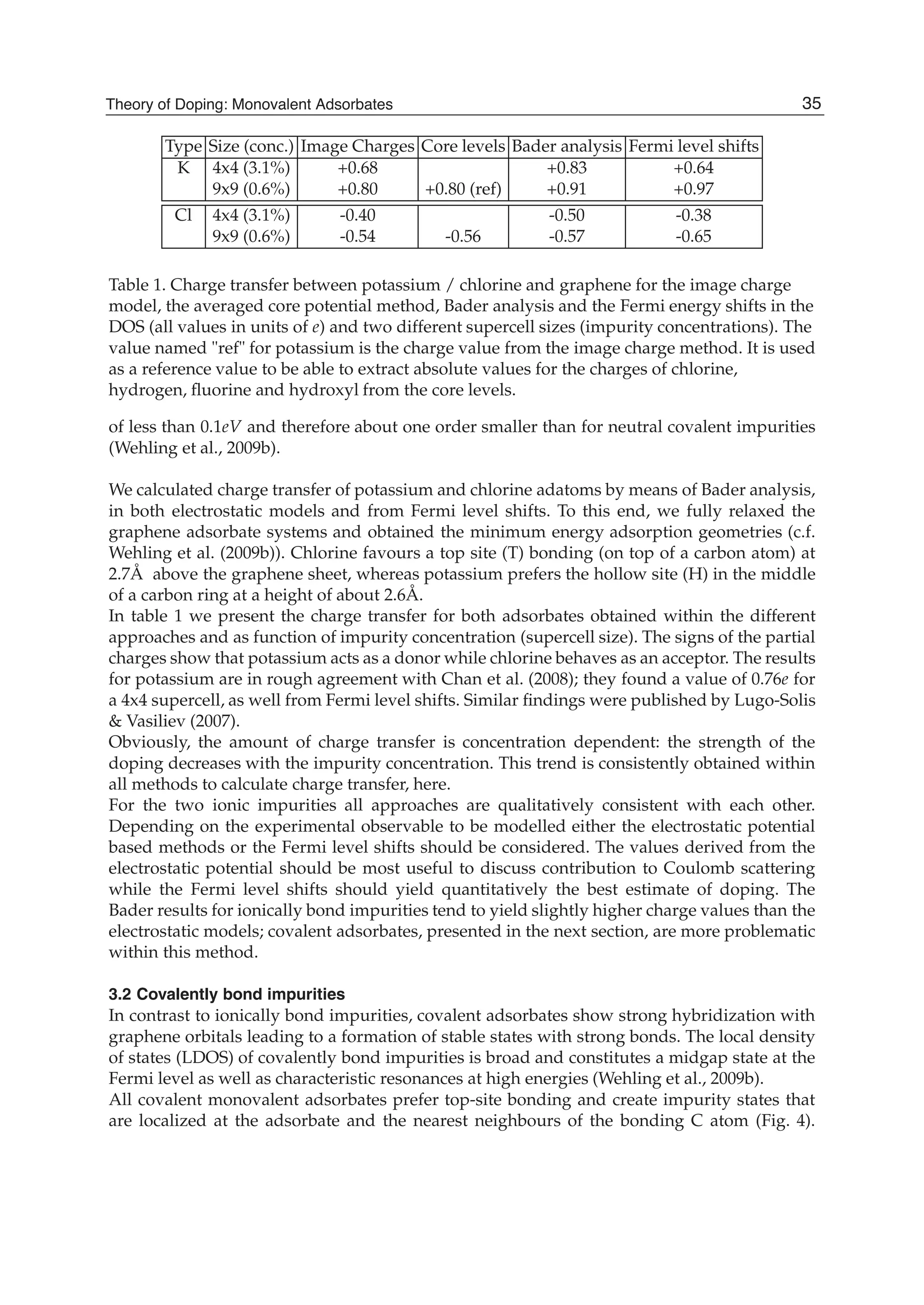
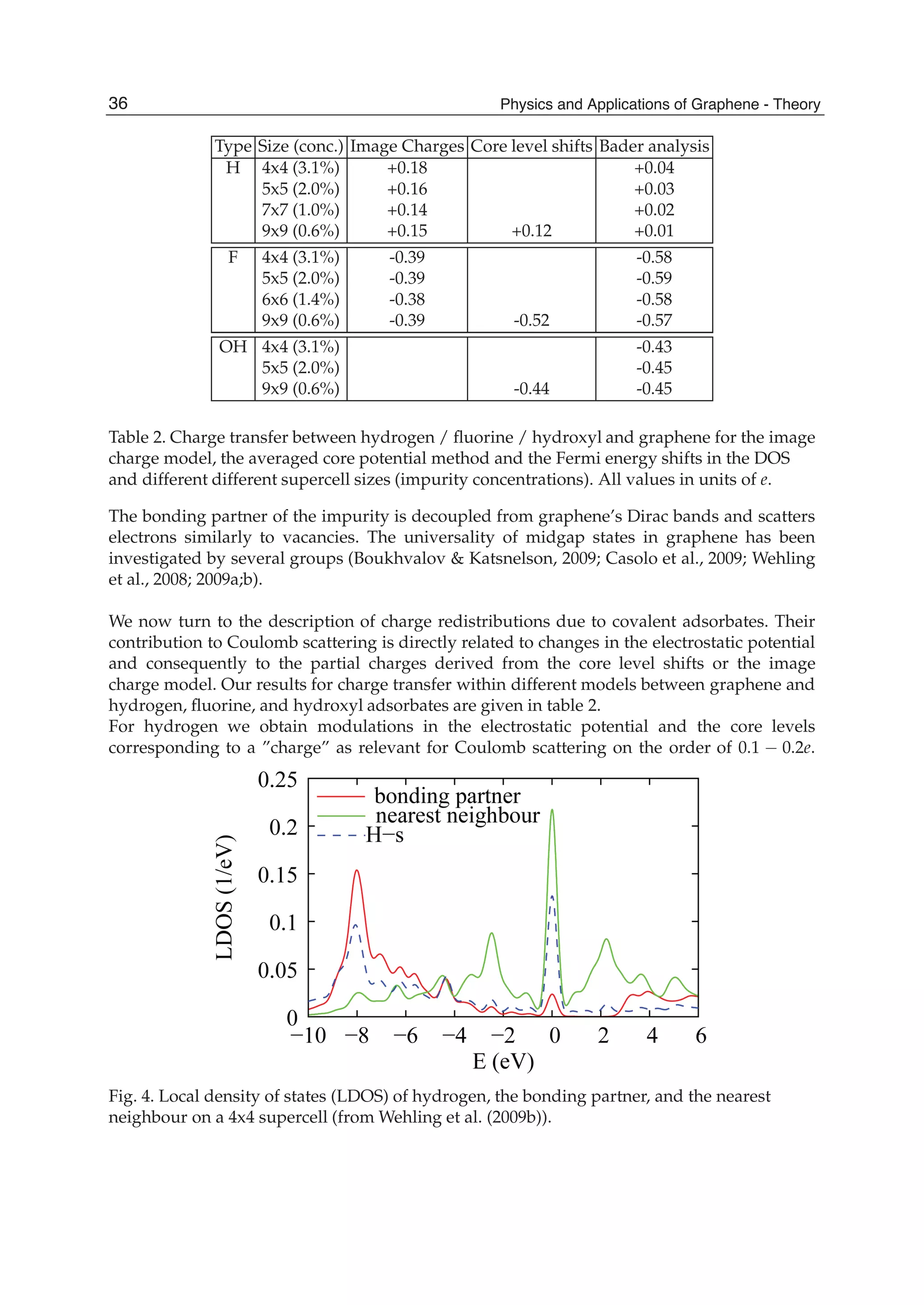
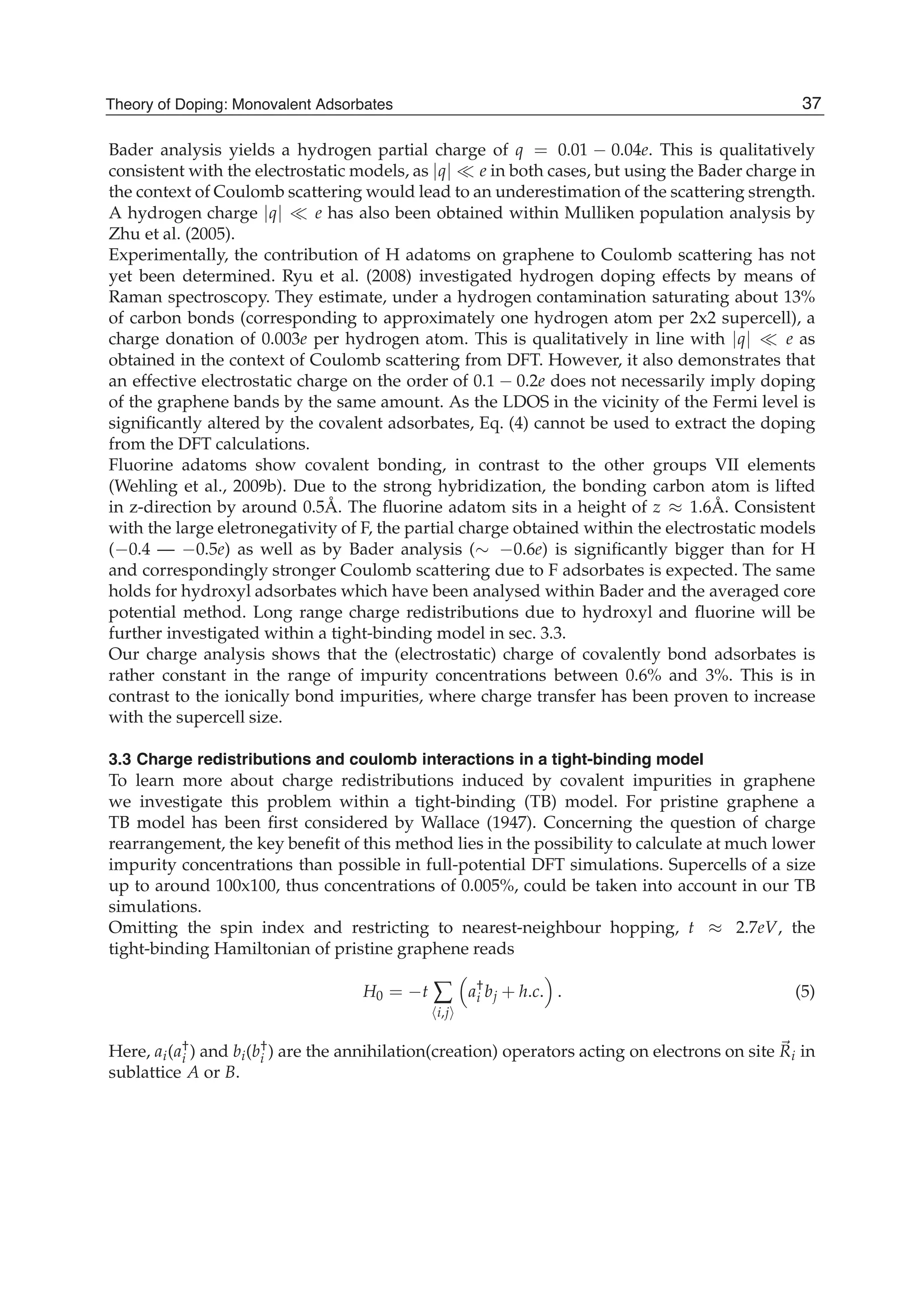
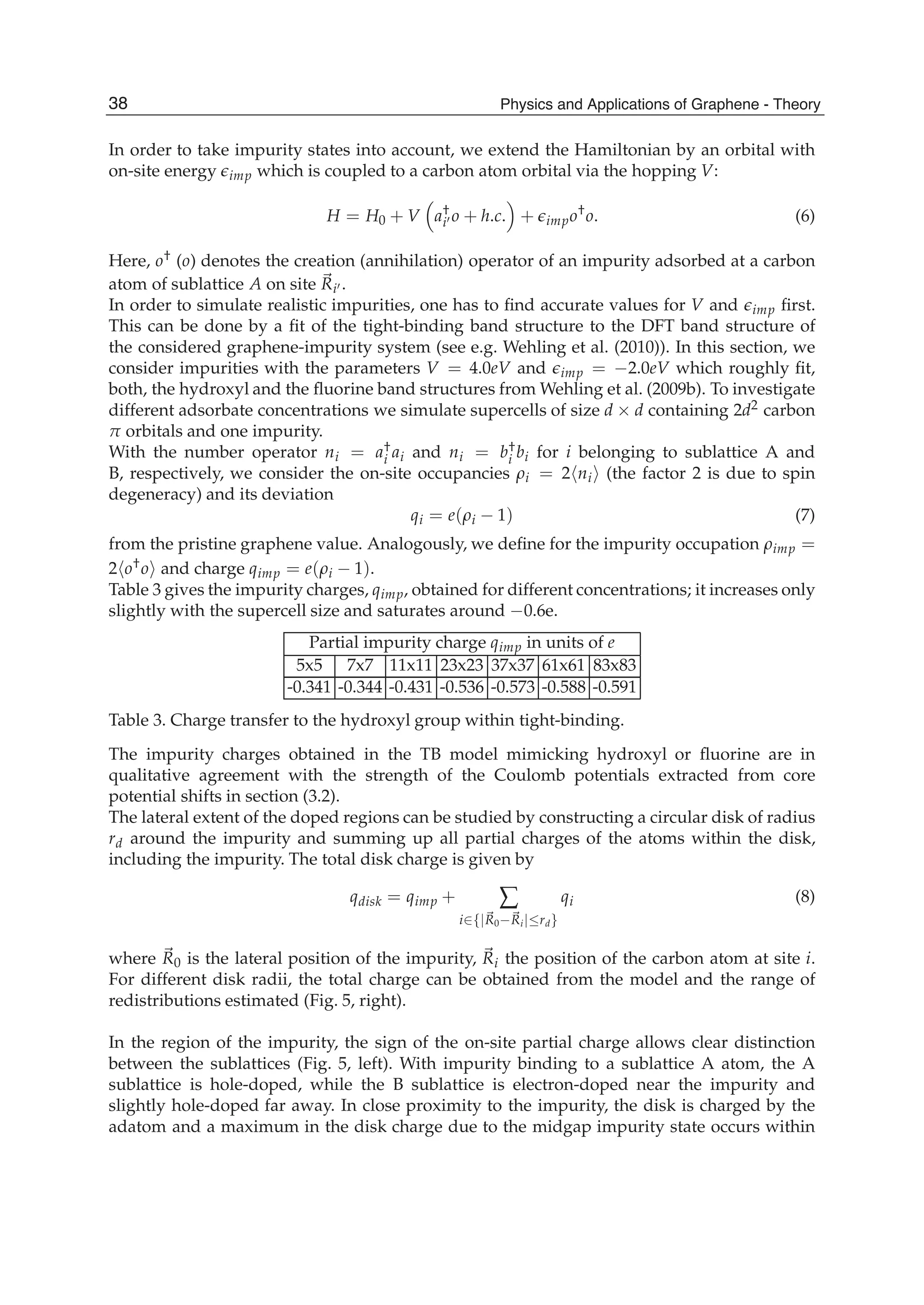
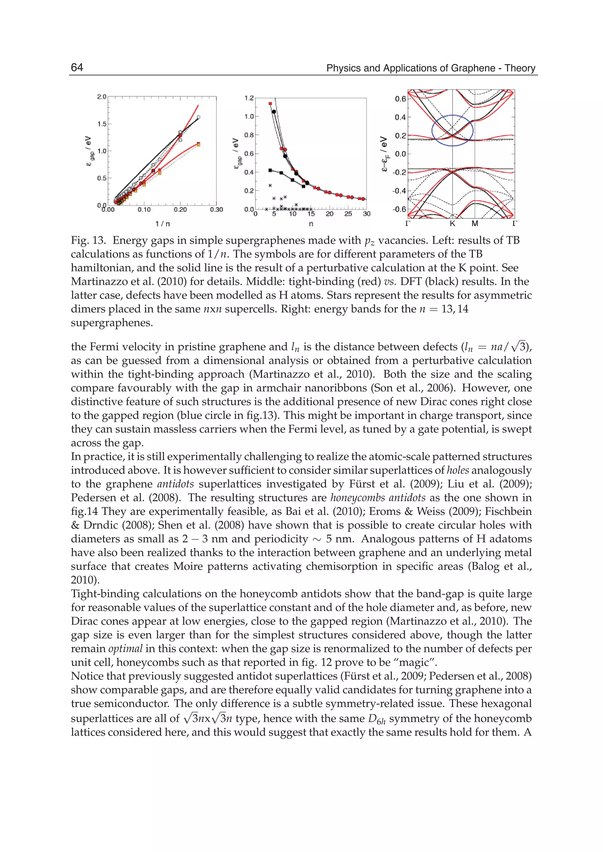
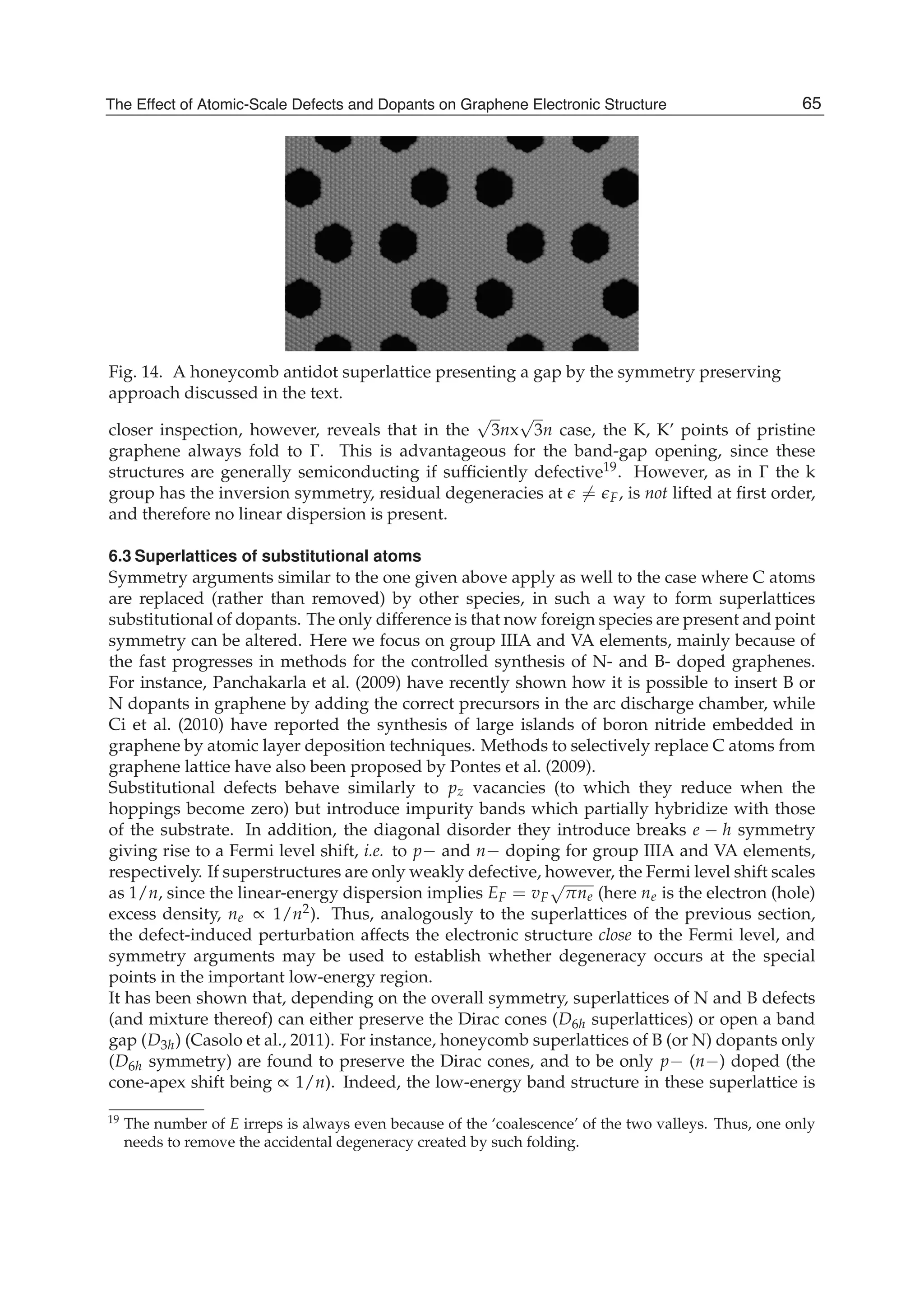
Downloaded 115 times


![Preface
The Stone Age, the Bronze Age, the Iron Age ... Every global epoch in the history of the
mankind is characterized by materials used in it. In 2004 a new era in the material sci-
ence was opened: the era of graphene or, more generally, of two-dimensional materials
[K. Novoselov, A. Geim et al. Science 306, 666 (2004)]. Graphene is the one-atom thin
layer of sp2
-bonded carbon atoms arranged in a honey-comb lattice. It possesses the
unique physical properties: graphene is the strongest and the most stretchable known
material, has the record thermal conductivity and the very high intrinsic mobility and
is completely impermeable. The charge carriers in graphene are the massless Dirac
fermions and its unique electronic structure leads to a number of interesting physical
effects, such as the minimal electrical conductivity, anomalous quantum Hall effect,
Klein tunneling, the universal optical conductivity and the strong nonlinear electro-
magnetic response. Graphene offers and promises a lot of different applications, in-
cluding conductive ink, terahertz transistors, ultrafast photodetectors, bendable touch
screens, strain tensors and many other. In 2010 Andre Geim and Konstantin Novoselov
were awarded the Nobel Prize in Physics “for groundbreaking experiments regarding
the two-dimensional material graphene”.
Nowadays, graphene is in the focus of research activity of condensed matter physi-
cists in the whole world. Research articles reporting on different aspects of graphene
studies are collected in the present two volumes “Physics and Applications of Gra-
phene”. These books cover a broad spectrum of experimental and theoretical studies
of graphene and present contributions from research groups and laboratories from the
North and South America, Europe, Asia and Australia.
The contributed articles are presented in two volumes. The readers interested in ex-
perimental studies of graphene are referred to the first volume. The second volume
contains theoretical contributions, divided into five Sections. In Part I ab initio studies
of the electronic structure of graphene in the presence of defects and impurities are
described. In Part II the theory of graphene nano-flakes and nano-ribbons is presented.
The magnetic properties of grapheme are discussed in Part III and the transport prop-
erties are studied in Part IV. The last Part of the volume is devoted to the linear and
nonlinear optical properties of graphene.
Sergey Mikhailov
University of Augsburg
Germany](https://image.slidesharecdn.com/grrphysicsandapplicationsofgraphene-theory-140422181144-phpapp02/75/physics-and_applications_of_graphene_-_theory-9-2048.jpg)


![Physics and Applications of Graphene - Theory26
Lin, C. S., R. Q. Zhang, et al. (2007). Geometric and Electronic Structures of Carbon
Nanotubes Adsorbed with Flavin Adenine Dinucleotide: A Theoretical Study. The
Journal of Physical Chemistry C,111,11, (4069-4073),1932-7447
Liu, S., S. Gangopadhyay, et al. (1997). Photoluminescence studies of hydrogenated
amorphous carbon and its alloys. Journal of Applied Physics,82,9, (4508-4514)
Loginova, E., N. C. Bartelt, et al. (2008). New J. Phys.,10, (16)
Loginova, E., N. C. Bartelt, et al. (2009). New J. Phys.,11, (20)
Loh, K. P., J. S. Foord, et al. (1996). Diamond Relat. Mater.,5, (231)
Malard, L. M., J. Nilsson, et al. (2007). Probing the electronic structure of bilayer graphene by
Raman scattering. Physical Review B,76,20, (201401)
Maniwa, Y., Y. Kumazawa, et al. (1999). Jpn. J. Appl. Phys.,38, (668)
Mann, D. J. and M. D. Halls (2003). Phys. Rev. Lett.,90, (195503)
Martí, J. and M. C. Gordillo (2001). Phys. Rev. E,64, (21504)
Martí, J. and M. C. Gordillo (2003). J. Chem. Phys.,119, (12540)
Martin, C. R. and P. Kohli (2003). The emerging field of nanotube biotechnology. Nat Rev
Drug Discov,2,1, (29-37),1474-1776
Mashl, R. J., S. Joseph, et al. (2003). Nano Lett.,3, (589)
McCann, E. and V. I. Fal'ko (2006). Landau-Level Degeneracy and Quantum Hall Effect in a
Graphite Bilayer. Physical Review Letters,96,8, (086805)
McCarty, K. F., P. J. Feibelman, et al. (2009). Carbon,47, (1806)
Mendes, R. C., E. J. Corat, et al. (1997). Diamond Relat. Mater.,6,, (490),
Muehldorf, A. V., D. Van Engen, et al. (1988). Aromatic-aromatic interactions in molecular
recognition: a family of artificial receptors for thymine that shows both face-to-face
and edge-to-face orientations. Journal of the American Chemical Society,110,19, (6561-
6562),0002-7863
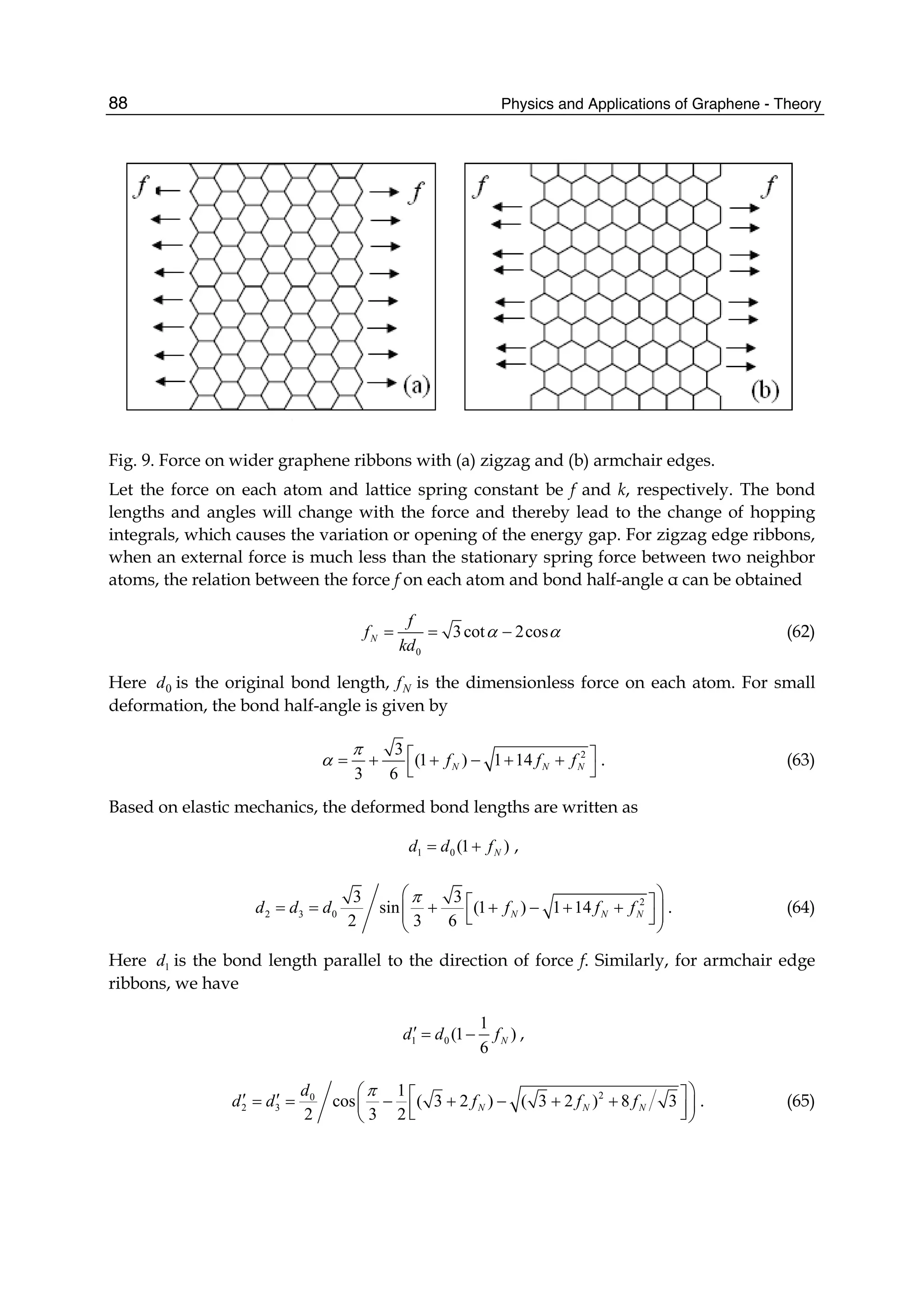
Nakada, K., M. Fujita, et al. (1996). Edge state in graphene ribbons: Nanometer size effect
and edge shape dependence. Physical Review B,54,24, (17954)
Nemanich, R. J., J. T. Glass, et al. (1988). Raman scattering characterization of carbon
bonding in diamond and diamondlike thin films. Journal of Vacuum Science &
Technology A: Vacuum, Surfaces, and Films,6,3, (1783-1787)
Nevin, W. A., H. Yamagishi, et al. (1994). Emission of blue light from hydrogenated
amorphous silicon carbide. Nature,368,6471, (529-531)
Noon, W. H., K. D. Ausman, et al. (2002). Chem. Phys. Lett.,355, (445)
Novoselov, K. S., A. K. Geim, et al. (2005). Nature,438, (197-200)
Novoselov, K. S., A. K. Geim, et al. (2004). Electric Field Effect in Atomically Thin Carbon
Films. Science,306,5696,(October 22, 2004) (666-669)
Novoselov, K. S., D. Jiang, et al. (2005). Proc. Natl. Acad. Sci. USA 102, (10451-10453)
Novoselov, K. S., E. McCann, et al. (2006). Unconventional quantum Hall effect and Berry/'s
phase of 2[pi] in bilayer graphene. Nat Phys,2,3, (177-180),1745-2473
Numata, M., M. Asai, et al. (2005). Inclusion of Cut and As-Grown Single-Walled Carbon
Nanotubes in the Helical Superstructure of Schizophyllan and Curdlan (β-1,3-
Glucans). Journal of the American Chemical Society,127,16, (5875-5884),0002-7863
O'Connell, M. J., S. M. Bachilo, et al. (2002). Band Gap Fluorescence from Individual Single-
Walled Carbon Nanotubes. Science,297,5581,(July 26, 2002) (593-596)
Ohta, T., A. Bostwick, et al. (2006). Controlling the Electronic Structure of Bilayer Graphene.
Science,313,5789,(August 18, 2006) (951-954)](https://image.slidesharecdn.com/grrphysicsandapplicationsofgraphene-theory-140422181144-phpapp02/75/physics-and_applications_of_graphene_-_theory-36-2048.jpg)
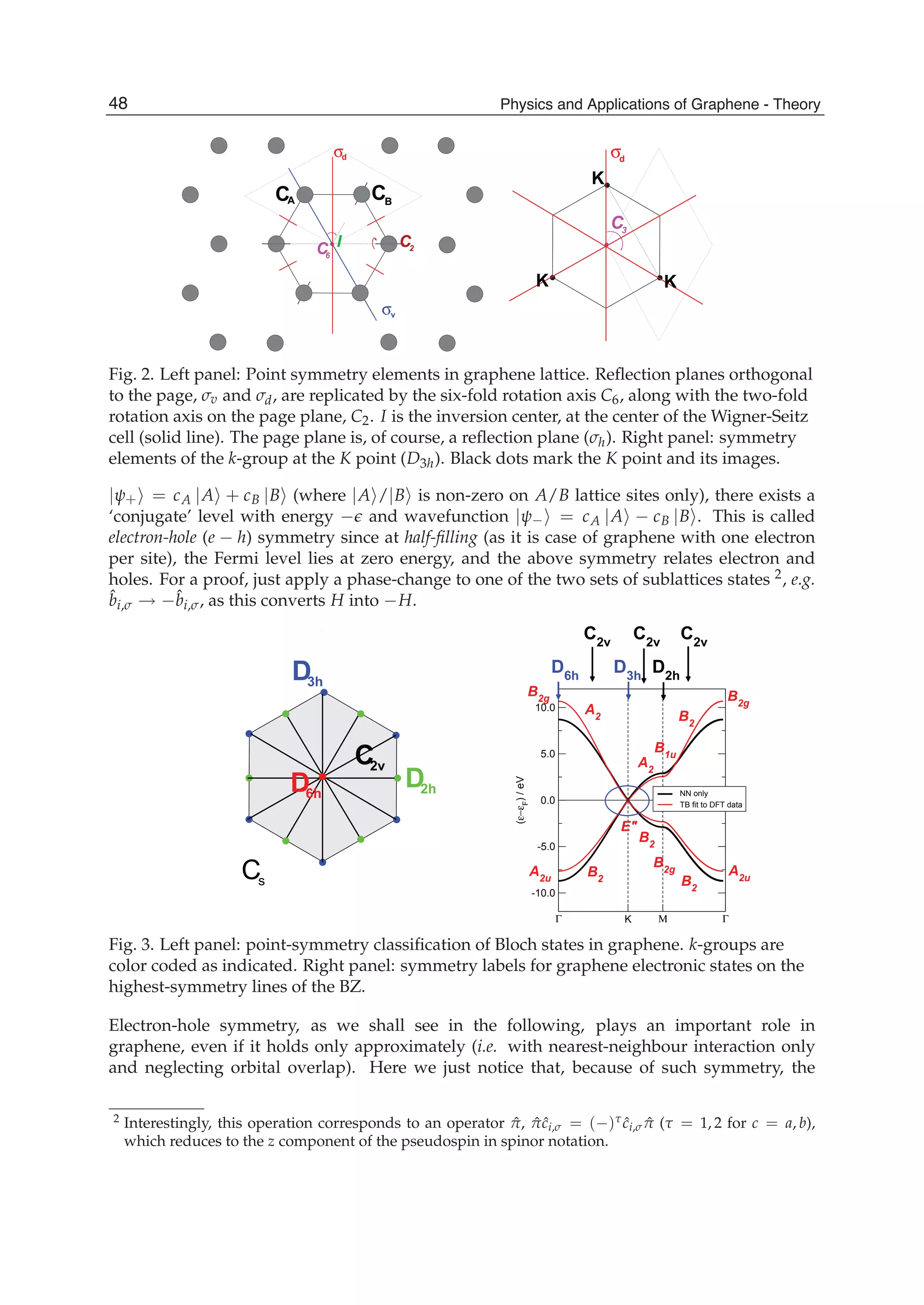
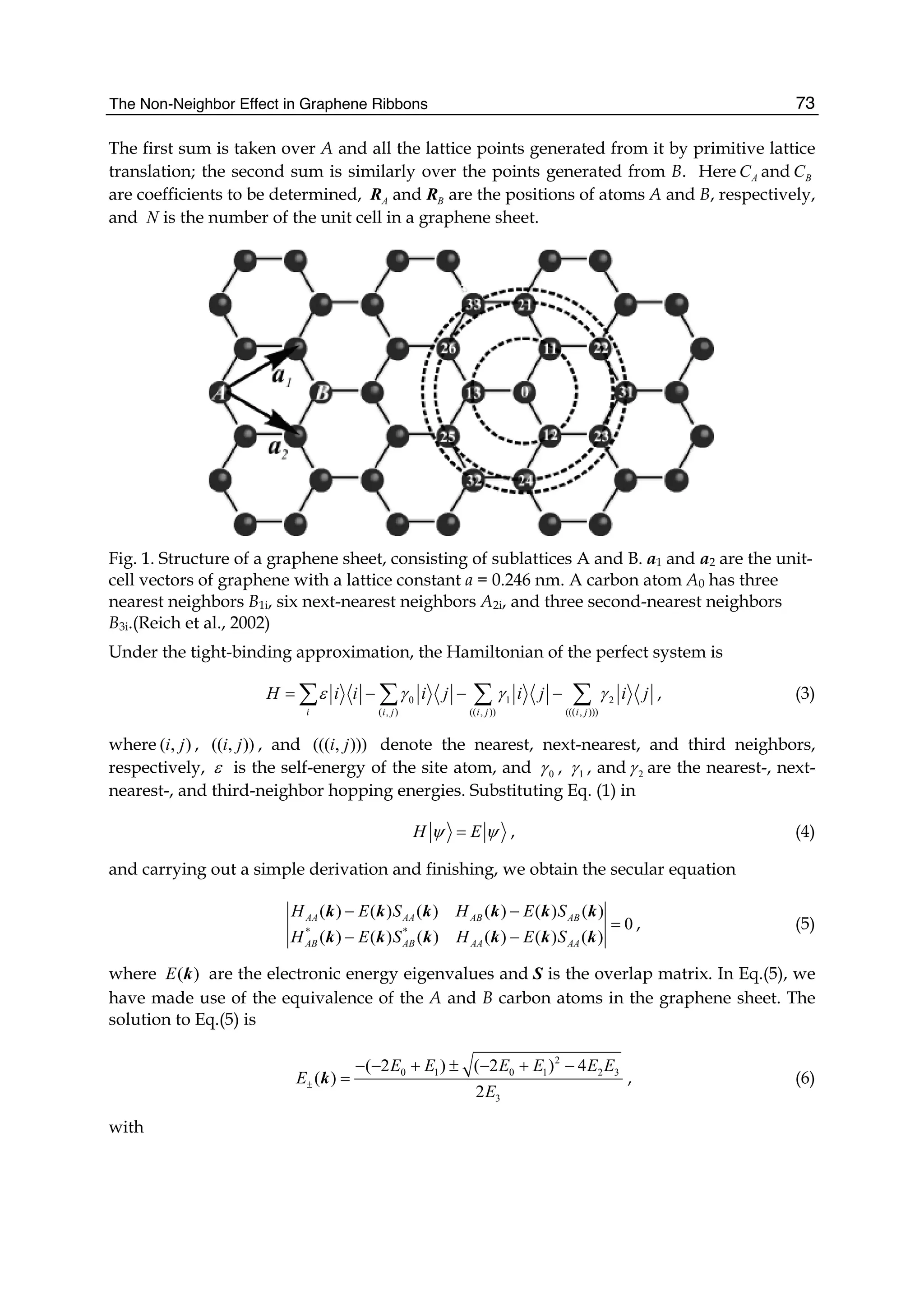
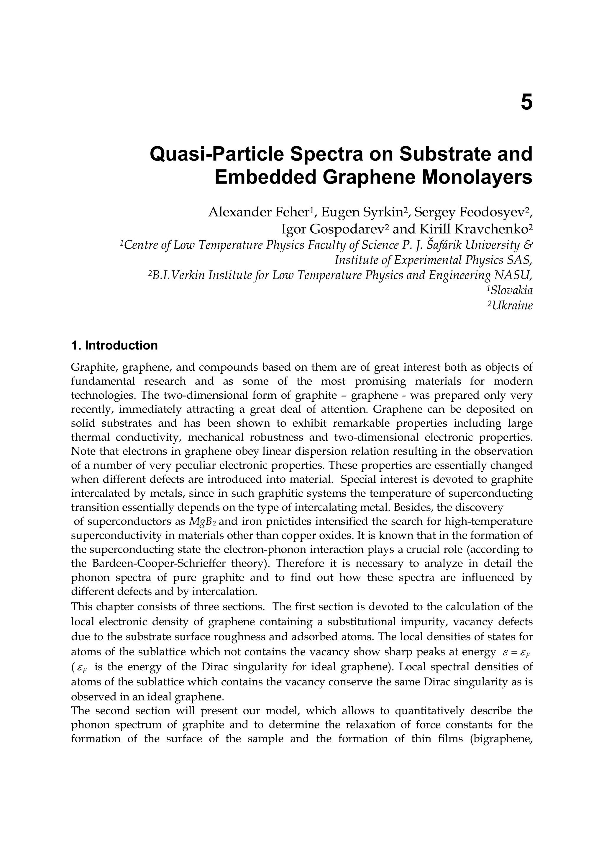
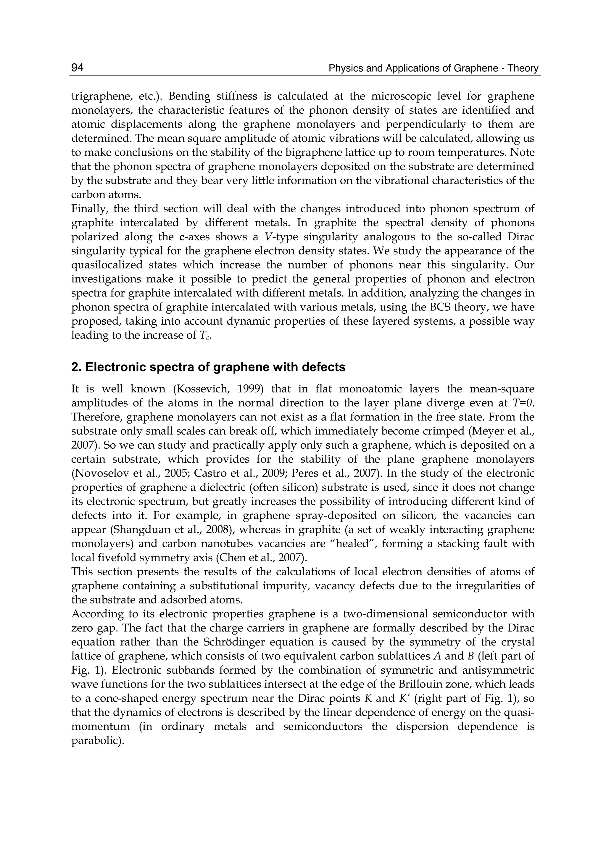
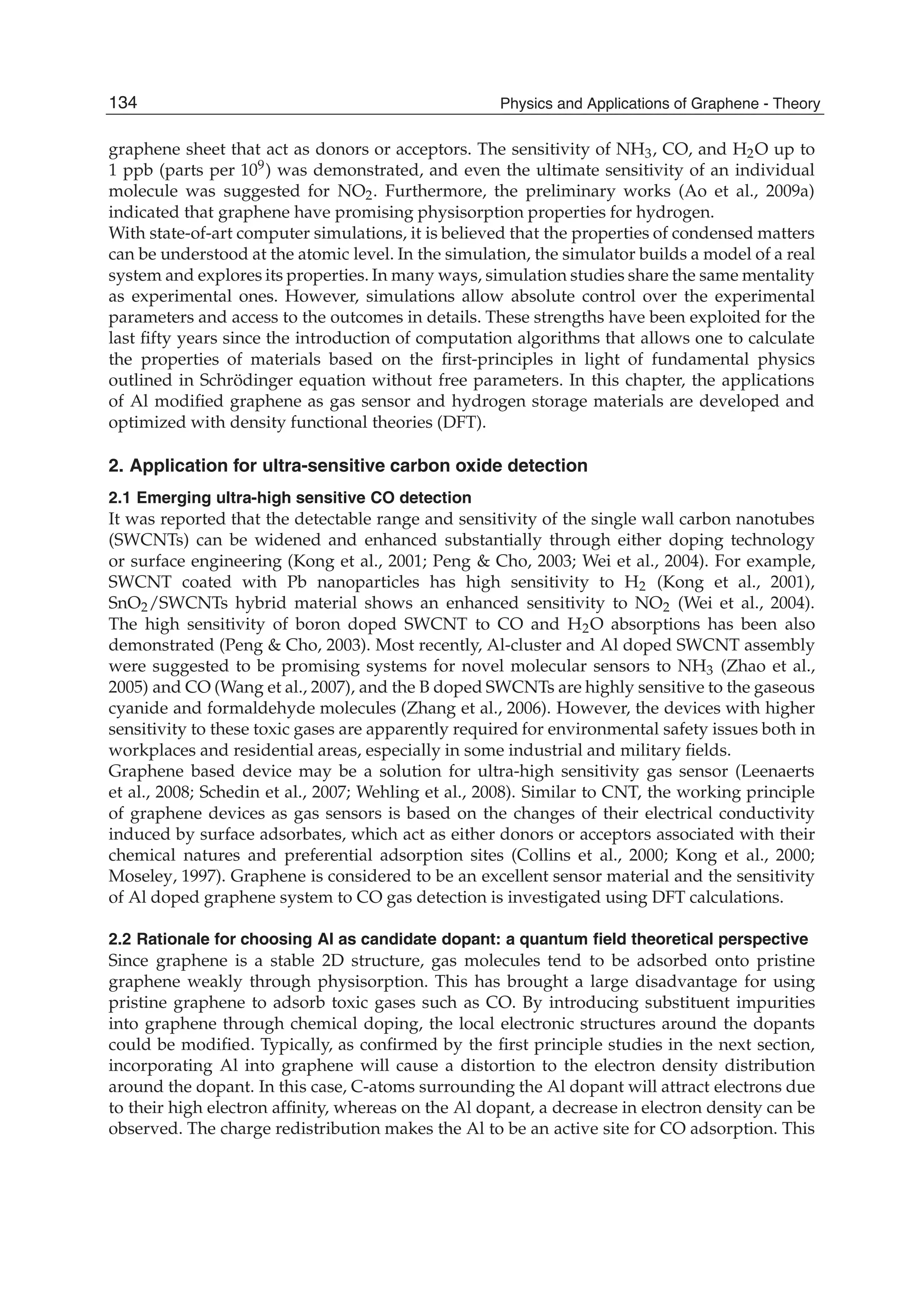
![and the second ones over sites which are nearest neighbours in each sublattice (t2 is the
corresponding hopping) 1. In absence of magnetic fields the hoppings can be chosen real,
and the accepted value for t1 is ∼ 2.7 eV while |t2| << t1 depends on the parametrization
used. Neglecting overlap between orbitals on different C atoms, the usual anticommutation
rules [ˆc†
i,σ, ˆc j,σ ]+ = δc,c δi,jδσ,σ (c = a, b) hold; hence, introducing the Fourier transformed
operators ˆak,σ according to
ˆai,σ =
1
√
N
∑
k∈BZ
e−ikRi ˆak,σ (4)
where the sum runs over k points in the first Brillouin zone (BZ) (analogously for ˆbk,σ) the
above Hamiltonian can be rewritten as
ˆHTB
= −t1 ∑
k,σ
f (k)ˆa†
k,σ
ˆbk,σ + h.c. − t2 ∑
k,σ
g(k)ˆa†
k,σ ˆak,σ − t2 ∑
k,σ
g(k)ˆb†
k,σ
ˆbk,σ (5)
or, in matrix notation,
ˆHTB
= − ∑
k,σ
ˆa†
k,σ, ˆb†
k,σ
t2g(k) t1 f (k)
t1 f ∗(k) t2g(k)
ˆak,σ
ˆbk,σ
Here f (k) and g(k) are ‘structure factors’ for the nearest- and next-nearest neighbours,
f (k) = ∑
i=1,3
e−ikδi
g(k) = ∑
i=1,6
e−ikδi
Diagonalization is trivial and gives the energy bands,
(k)± = −t2g(k) ± t1|f (k)| = −t2g(k) ± t1 3 + g(k) (6)
where |f (k)|2 = 3 + g(k) has been used and the minus (plus) sign solution correspond to the
π (π∗) band (see e.g. Bena & Montambaux (2009); Castro Neto et al. (2009); Wallace (1947)).
Close to the K(K ) point |f (K + q)|2 ∼ v2
Fq2 and the dispersion is conical, giving rise to the
so-called Dirac cones. Here vF =
√
3
2 a = 3
2 d, where d is the carbon-carbon distance, ∼ 1.42
Å, and a the lattice constant. Consequently, the density-of-states (DOS) is linearly vanishing
at zero energy, ρ( ) ∼ 2| |/π
√
3t2, one of the fingerprints of massless Dirac electrons. Its
vanishing value challenges one’s intuition since experiments find a finite, non-zero minimum
conductivity at this energy (Peres, 2010).
Albeit simple, this tight-binding model is accurate enough to correctly represent graphene π
bands, at least close to the high symmetry points K and K . The latter control the low-energy
physics of charge carriers, and are the source of the exceptional interest in graphene. If only
nearest-neighbours interaction is allowed the two sublattices form two disjoint sets where
A-type sites connect to B-type sites only and vice versa. The Hamiltonians is said bipartitic
and displays an interesting symmetry: for each non-zero energy level and eigenfunction
1 Notice that the on-site energies (the energy of carbon pz orbitals) have been set equal to zero, but
additional terms of the form ∑i i ˆc†
i ˆci would appear if graphene were subjected to an inhomogeneous
external potential.
47The Effect of Atomic-Scale Defects and Dopants on Graphene Electronic Structure](https://image.slidesharecdn.com/grrphysicsandapplicationsofgraphene-theory-140422181144-phpapp02/75/physics-and_applications_of_graphene_-_theory-57-2048.jpg)

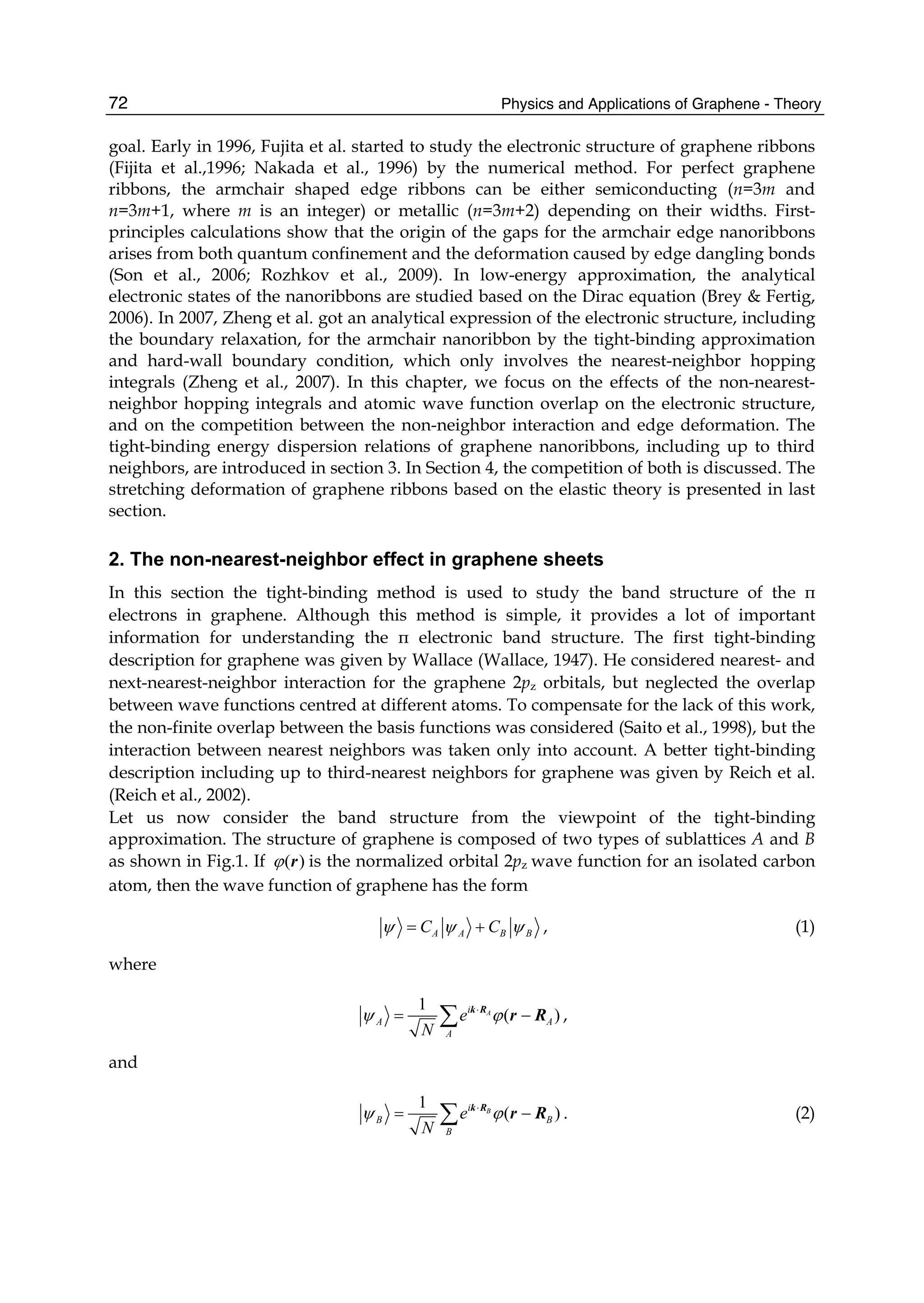
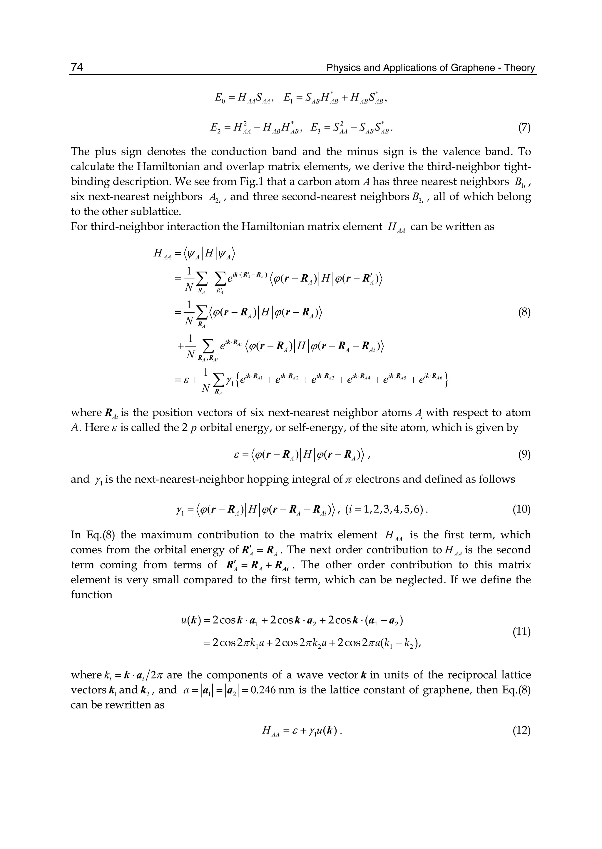
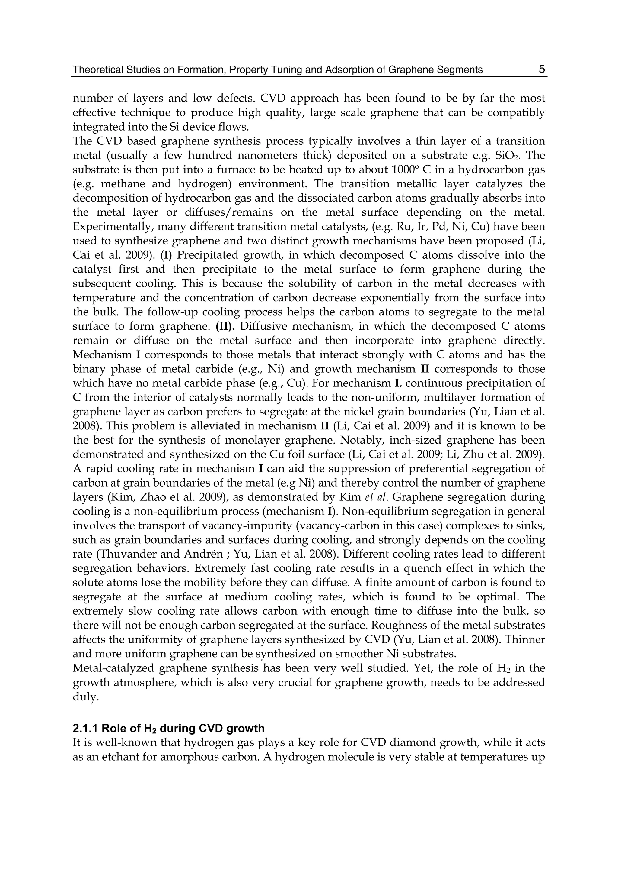
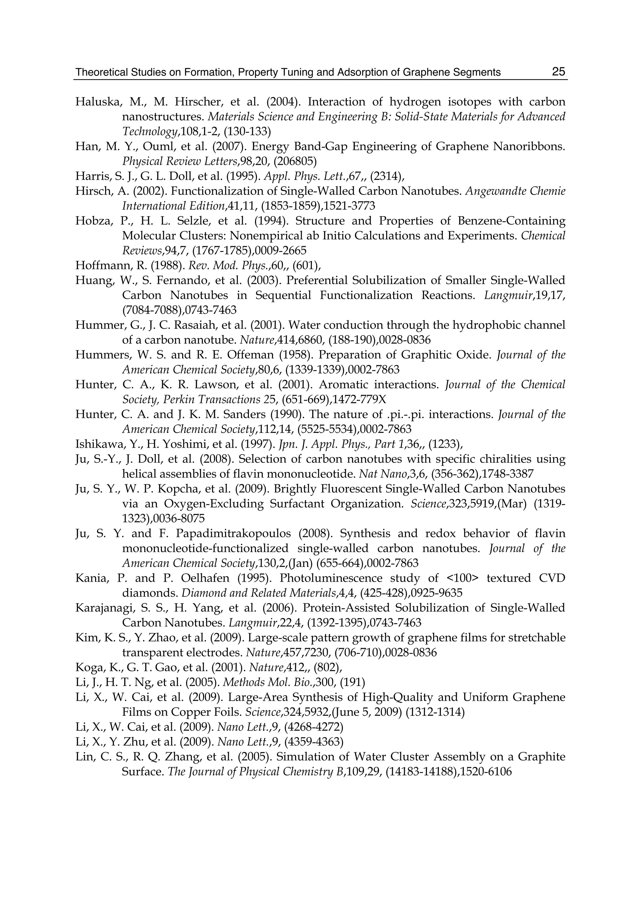
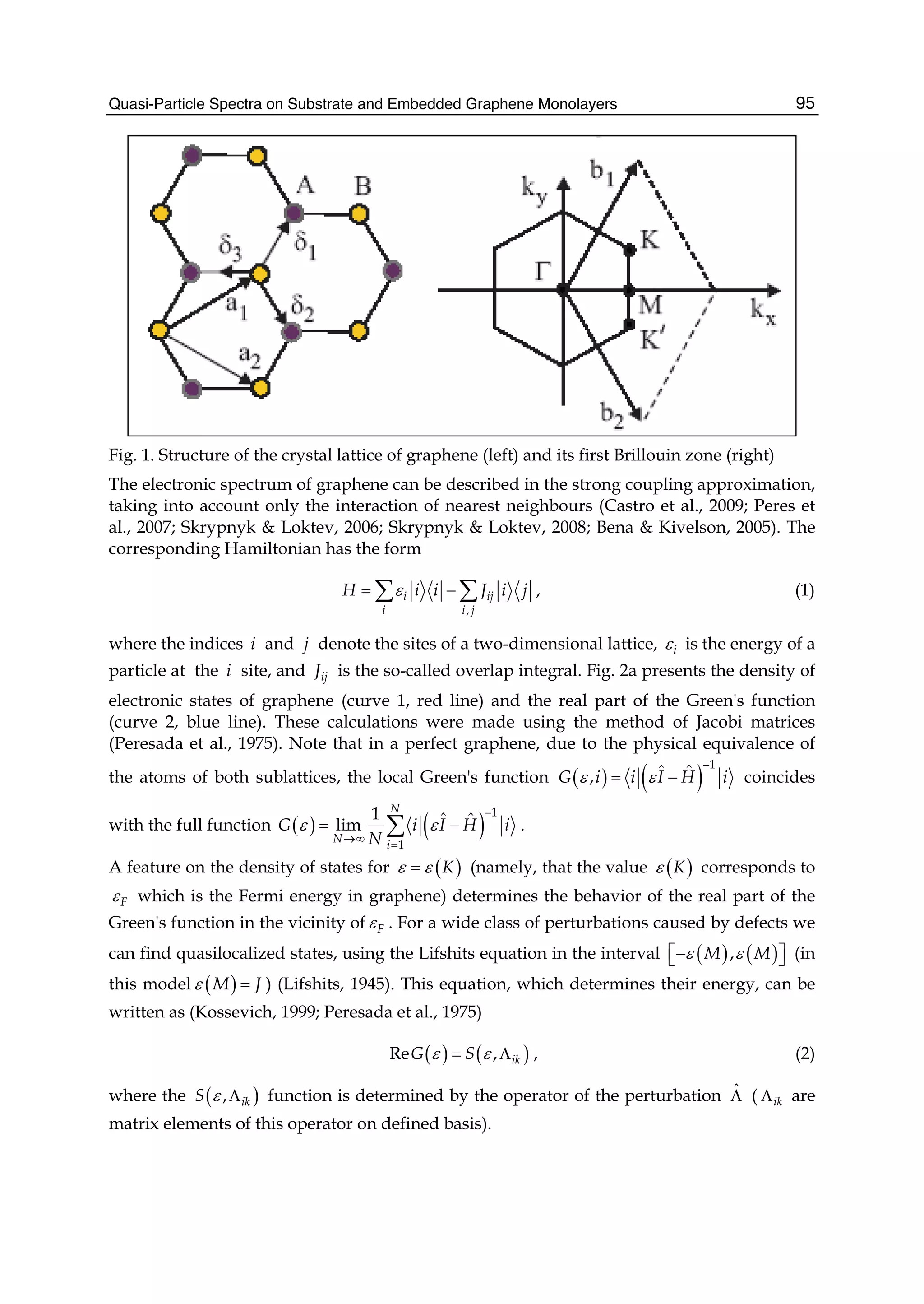
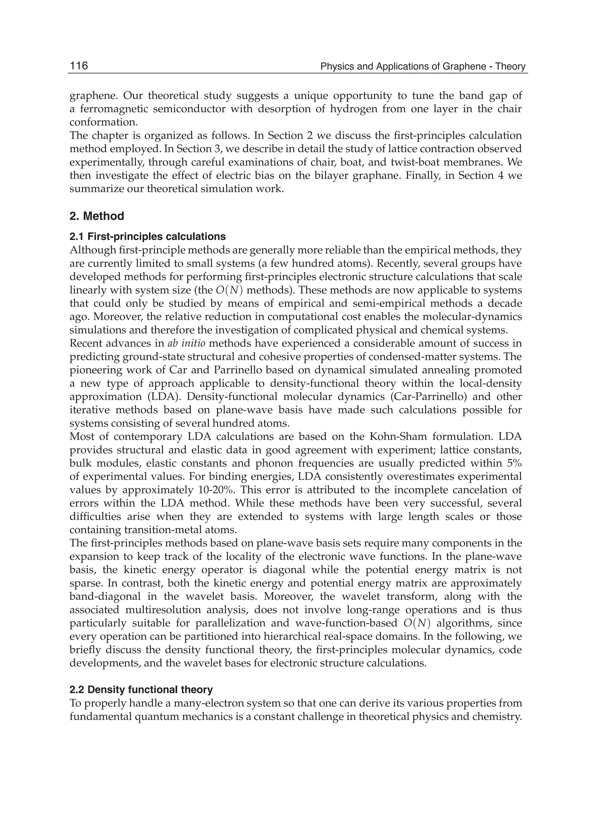
![Physics and Applications of Graphene - Theory76
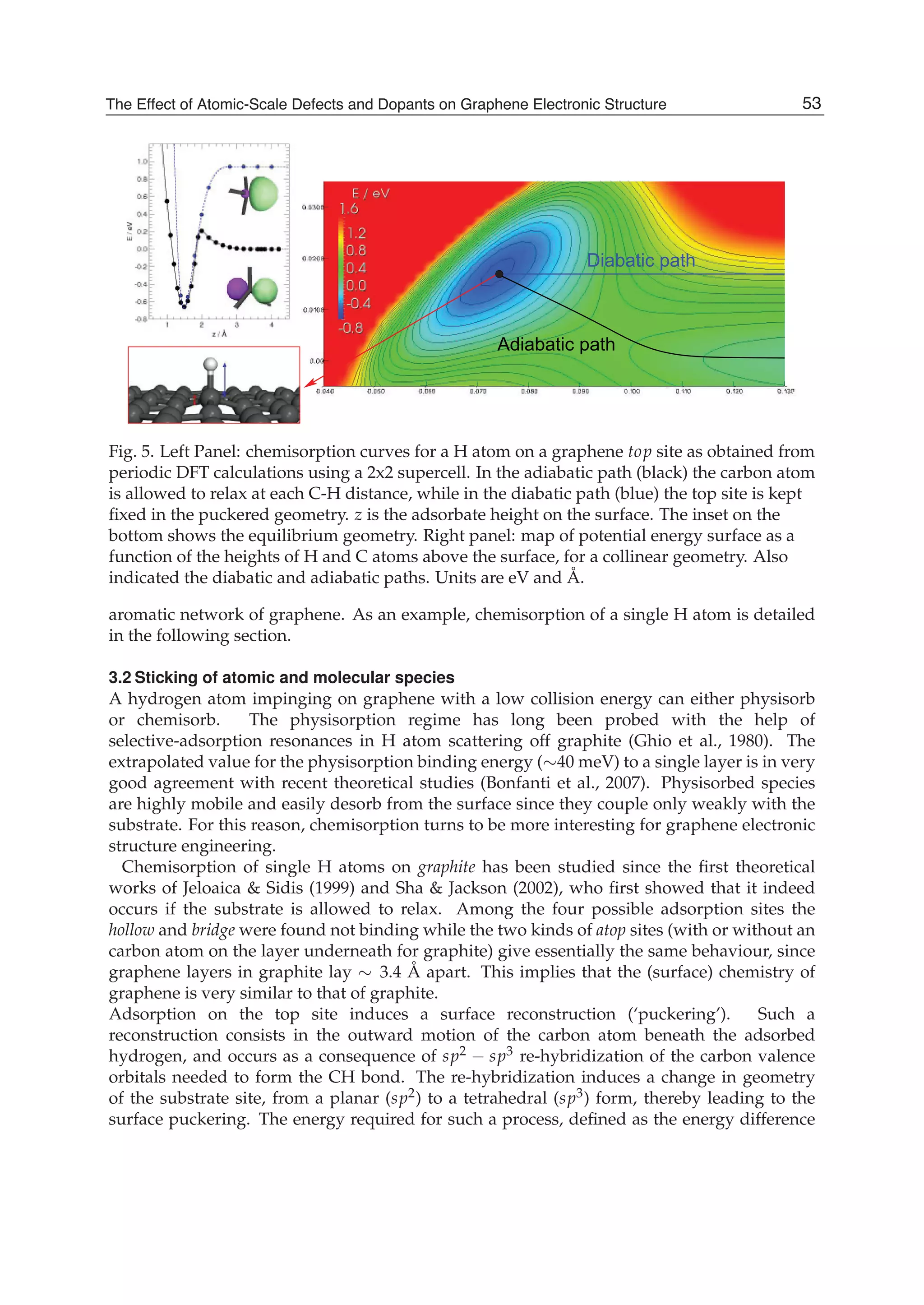
0 1 1[ ( )][1 ( )]E u s uε γ= + +k k , (21)
1 0 0 0 2 2 0 2 22 [3 ( )] ( ) ( ) 2 [3 (2 )]E s u s s g s uγ γ γ γ= + + + + +k k k , (22)
2 2 2
2 1 0 0 2 2[ ( )] [3 ( )] ( ) [3 (2 )]E u u g uε γ γ γ γ γ= + − + − − +k k k k , (23)
2 2 2
3 1 0 0 2 2[1 ( )] [3 ( )] ( ) [3 (2 )]E s u s u s s g s u= + − + − − +k k k k , (24)
where
1 2 1 2( ) 2 ( ) (2 , 2 )g u u k k k k= + − −k k .
Inserting 0E to 3E into Eq.(6) we can obtain the tight-binding energy dispersion relation in the
third-neighbor approximation.
To give the numerical results of energy dispersion, we must know the values of the hopping
energies and overlap integrals. We take the parameters 0.28ε = − eV, 0 2.97γ = − eV,
1 0.073γ = − eV, 2 0.33γ = − eV, 0 0.073s = , 1 0.018s = , and 2s =0.026 (Reich et al., 2002). The
computed results for some high-symmetry points (KΓM) are shown in Fig. 2, where the solid
line denotes the nearest-neighbor result, the dashed line represents the next-nearest-
neighbor, and the dotted line is the third-neighbor. It is clear that the next-nearest-neighbor
hopping integrals and overlap between atomic wave functions will play an important role
on the band width at Γ point, which can largely reduce the bandwidth, and the third-
neighbor interaction can slightly enhance the bandwidth. But the role of both is just opposite
for M point. It is worth pointing out that when we take only into account the nearest
neighbor hopping integral and let both the overlap s0 and the site energy ε be zero, the
energy bands are symmetric with respect to the Fermi level. The nearest neighbor result in
Fig. 2 is to include the overlap s0, so the energy bands become asymmetric, leading to the
Fig. 2. Tight-binding energy bands of graphene for high-symmetry points. The solid line
denotes the nearest neighbor, the dashed line represents the next-nearest neighbor, and the
dotted line is the third neighbor.](https://image.slidesharecdn.com/grrphysicsandapplicationsofgraphene-theory-140422181144-phpapp02/75/physics-and_applications_of_graphene_-_theory-86-2048.jpg)
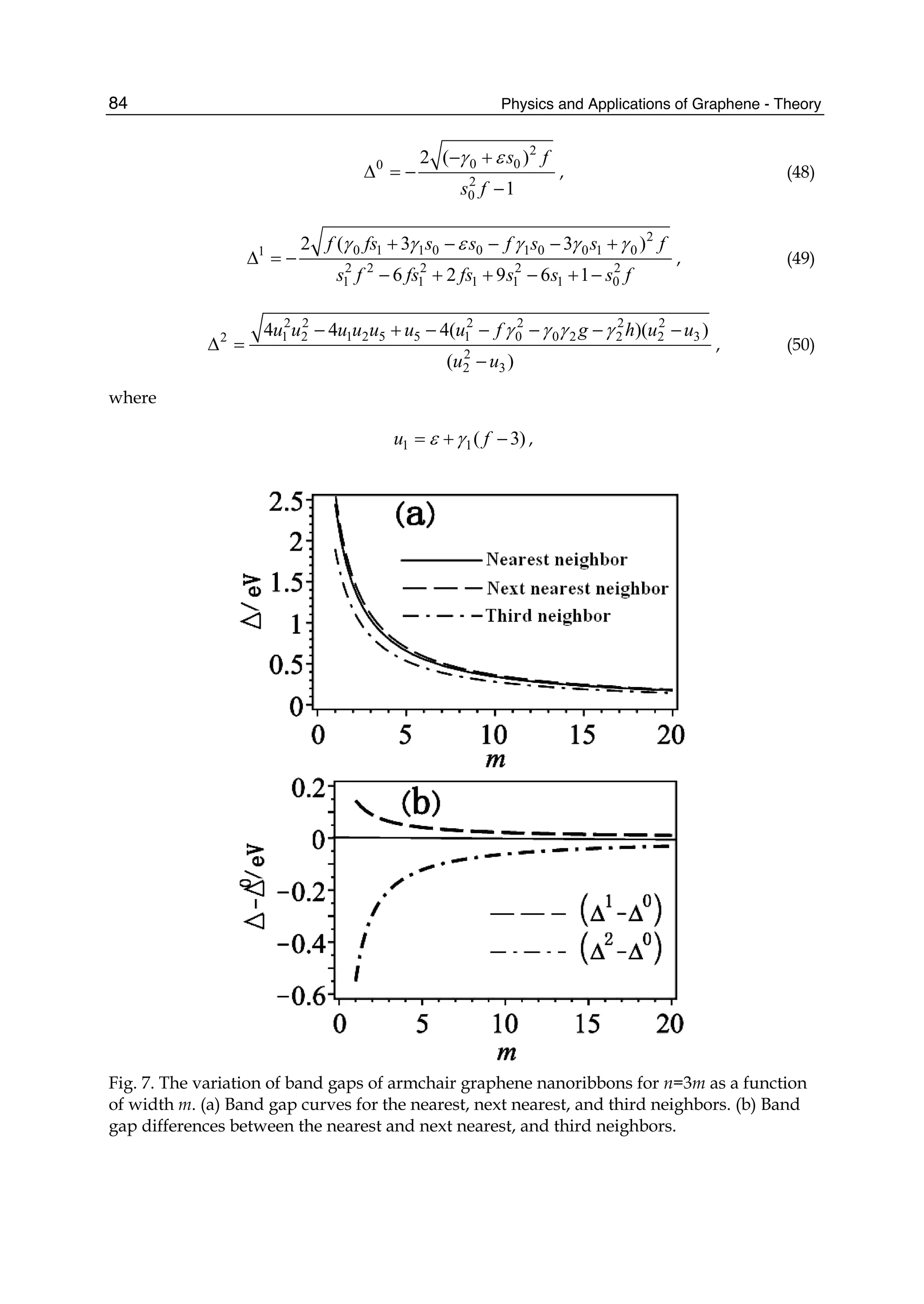
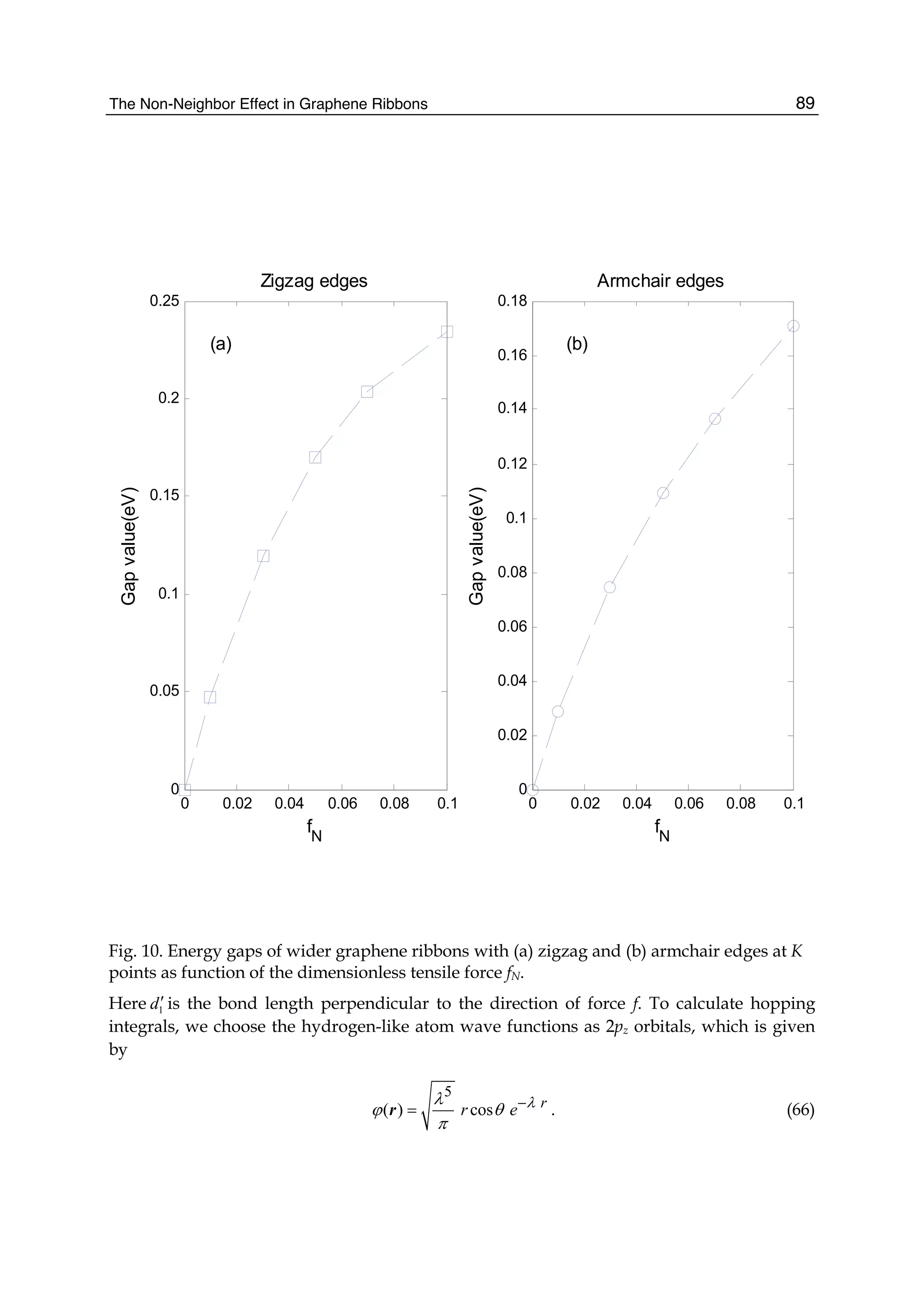
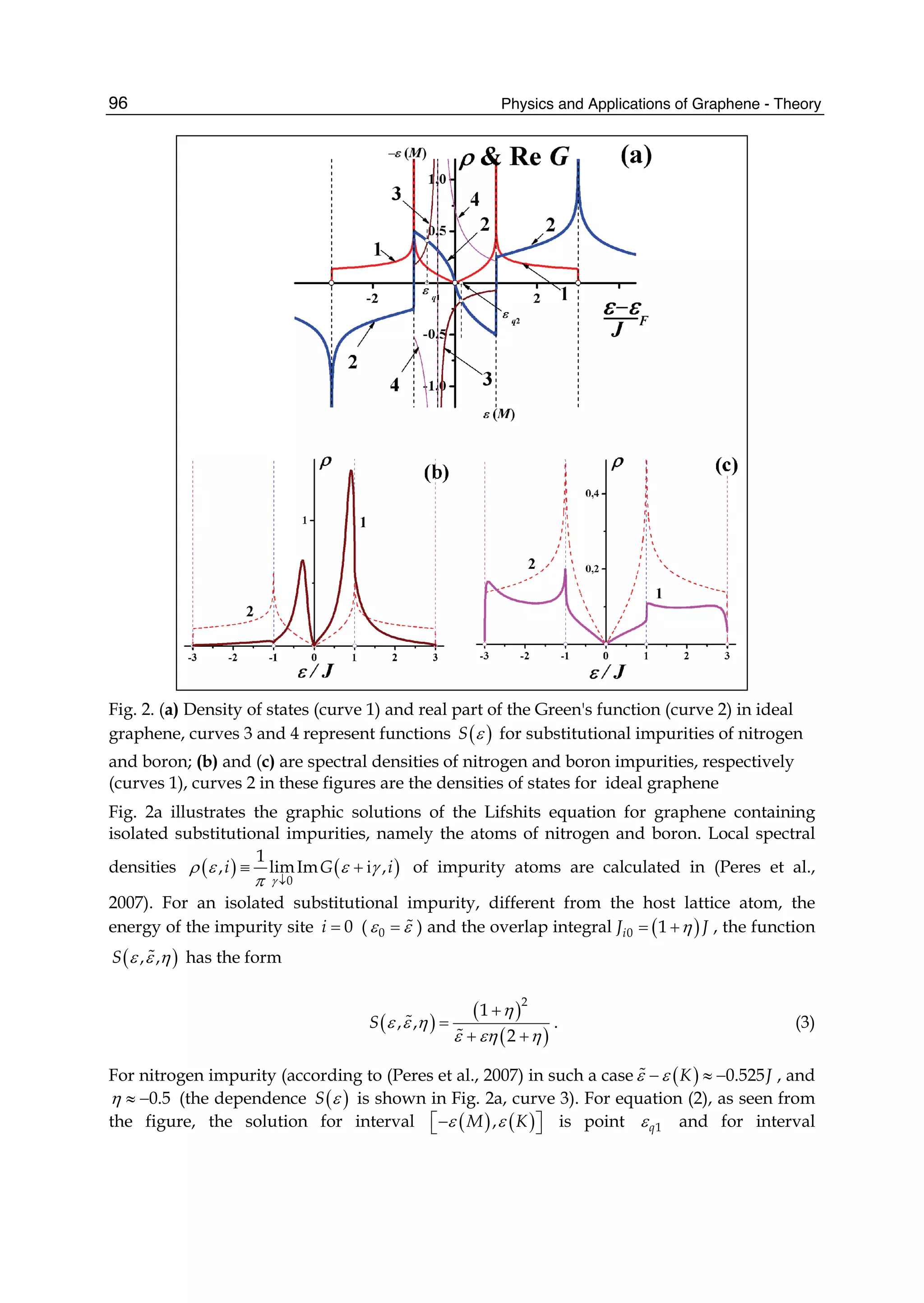
![The Non-Neighbor Effect in Graphene Ribbons 79
2
0 1 0 1 2 3
3
( 2 ) ( 2 ) 4
( , )
2
x
E E E E E E
E k q
E
±
− − + ± − + −
= , (32)
where
0 1 1( , ) { [ ( , ) 3]}{[1 [ ( , ) 3]}x x xE k q f k q s f k qε γ= + − + − , (33)
1 0 0 0 2 2 0 2 2( , ) 2 ( , ) ( ) ( , ) 2 ( , )x x x xE k q s f k q s s g k q s h k qγ γ γ γ= + + + , (34)
2 2 2
2 1 0 0 2 2( , ) { [ ( , ) 3]} ( , ) ( , ) ( , )x x x x xE k q f k q f k q g k q h k qε γ γ γ γ γ= + − − − − , (35)
2 2 2
3 1 0 0 2 2( , ) {1 [ ( , ) 3]} ( , ) ( , ) ( , )x x x x xE k q s f k q s f k q s s g k q s h k q= + − − − − , (36)
and
23
( , ) 1 4cos cos 4cos
1 2 1
x
x
q k a q
f k q
n n
π π⎛ ⎞ ⎛ ⎞ ⎛ ⎞
= + +⎜ ⎟ ⎜ ⎟ ⎜ ⎟
+ +⎝ ⎠ ⎝ ⎠ ⎝ ⎠
,
( ) 22 2
( , ) 1 4cos cos 3 4cos
1 1
x x
q q
h k q k a
n n
π π⎛ ⎞ ⎛ ⎞
= + +⎜ ⎟ ⎜ ⎟
+ +⎝ ⎠ ⎝ ⎠
,
3 3 3 3
( , ) 2 ( , ) 2cos 2cos 2cos(3 ) 6
2 1 2 1
x x
x x x
k a q k a q
g k q f k q k a
n n
π π⎛ ⎞ ⎛ ⎞
= + + + − + −⎜ ⎟ ⎜ ⎟
+ +⎝ ⎠ ⎝ ⎠
.
The electronic dispersion given by Eq. (32), in form, is exactly the same as that found for a
graphene sheet, but both have the difference in nature (Jin et al., 2009). The
region 3 3π π− ≤ ≤xk a is within the first Brillouin zone. These results are valid for various
energy ranges.
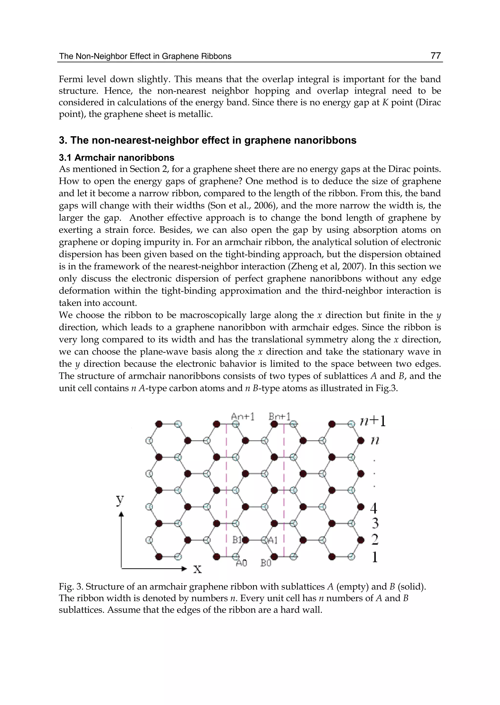
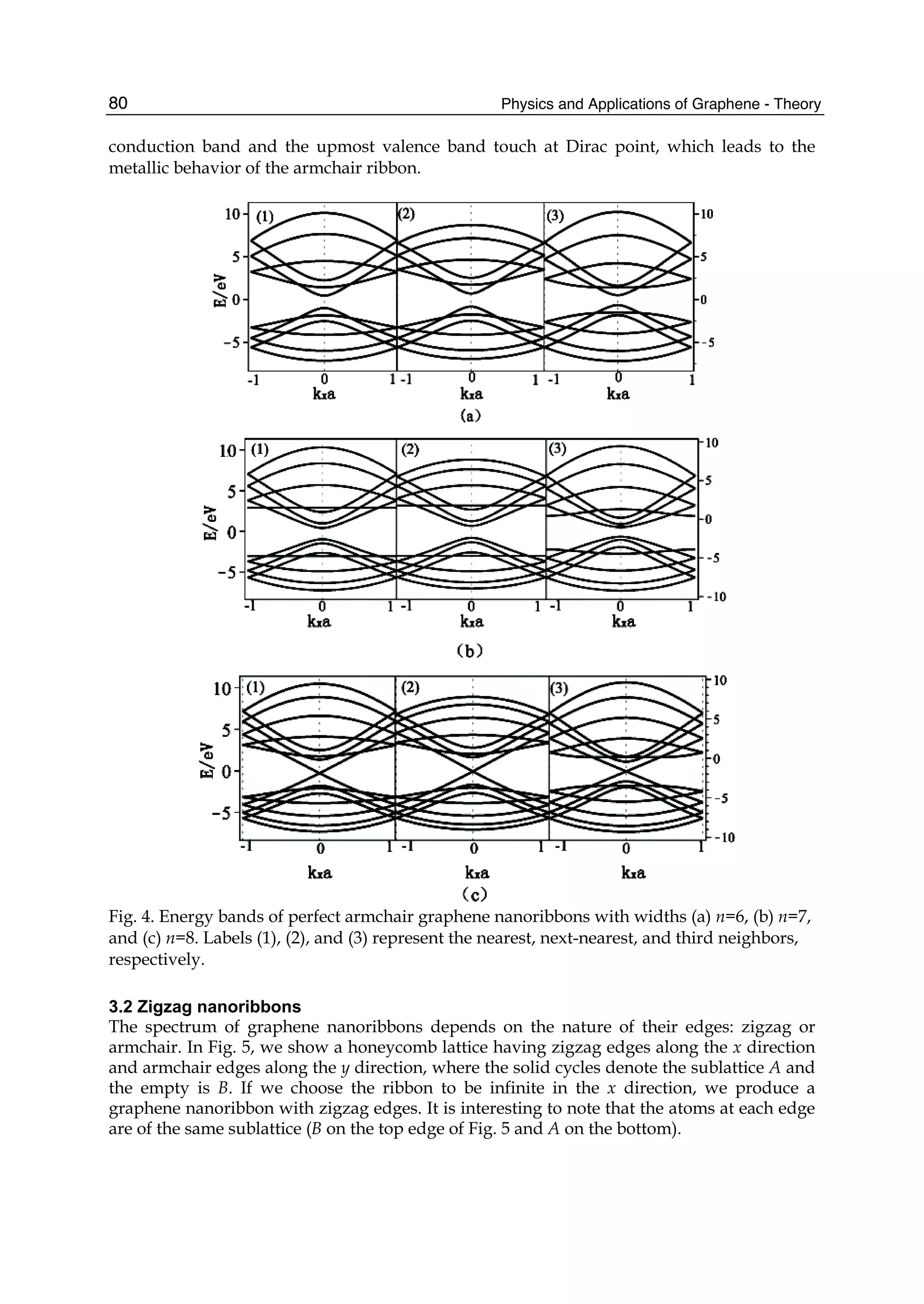
Since the electronic structure of perfect armchair graphene nanoribbons depends strongly
on the width of the ribbon, the system, for instance, is metallic when n=3m+2 (m is an
integer) and is insulating otherwise. To give a graph of energy bands, we still use the same
parameter values as taken in a graphene sheet. The electronic energy bands of the armchair
nanoribbons with three different widths are plotted in Fig.4, where (a) is n=3m=6, (b)
n=3m+1=7, and (c) n=3m+2=8. Labels (1), (2), and (3) denote the nearest, next-nearest, and
third neighbors, respectively. As 6=n and 7=n , the armchair ribbons appear insulating.
Fig.4 shows that the next-nearest-neighbor hopping and overlap integral would give rise to
change of the energy band width. This is because the energy levels of the conduction band
top are squeezed, which correspond to the stationary waves with small q values. The third
neighbors not only affect the energy gaps, such as n=6 and n=7, but also the band widths.
The influence on the band width mainly is because the bands related to the standing waves
with small q values in conduction and valence band produce a larger bend and this effect
was particularly evident when n=7,8. However, the effect on the energy gaps is because the
bands corresponding to larger q go down slightly. It is worth noting that when 7n = , there
is a flat conduction or valence band, taking not into account the third neighbors, which
corresponds to the quantum number q=(n+1)/2. Such a flat band is independent of wave
vector kx and in general exists only when n is equal to odd. As for 8=n , the lowest](https://image.slidesharecdn.com/grrphysicsandapplicationsofgraphene-theory-140422181144-phpapp02/75/physics-and_applications_of_graphene_-_theory-89-2048.jpg)
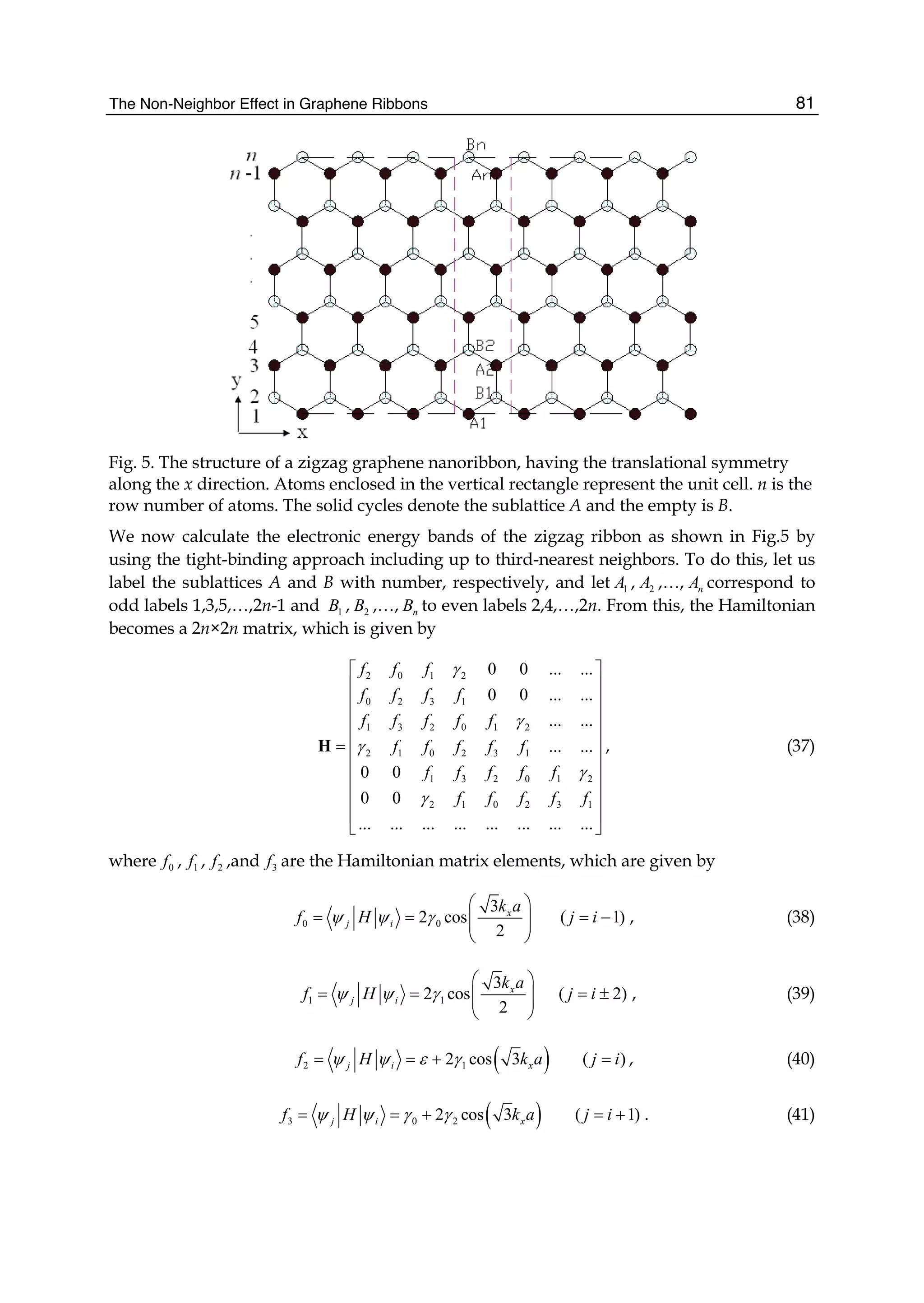
![Physics and Applications of Graphene - Theory82
0γ , 1γ , and 2γ are the nearest-, next-nearest-, and third-neighbor electronic hopping
amplitudes, respectively. Similarly, the overlap matrix S can be written as
2 0 1 2
0 2 3 1
1 3 2 0 1 2
2 1 0 2 3 1
1 3 2 0 1 2
2 1 0 2 3 1
0 0 ... ...
0 0 ... ...
... ...
... ...
0 0
0 0
... ... ... ... ... ... ... ...
g g g s
g g g g
g g g g g s
S s g g g g g
g g g g g s
s g g g g g
⎡ ⎤
⎢ ⎥
⎢ ⎥
⎢ ⎥
⎢ ⎥
= ⎢ ⎥
⎢ ⎥
⎢ ⎥
⎢ ⎥
⎢ ⎥
⎣ ⎦
, (42)
where
0 0
3
2 cos
2
x
j i
k a
g sψ ψ
⎛ ⎞
= = ⎜ ⎟⎜ ⎟
⎝ ⎠
( 1)j i= − , (43)
1 1
3
2 cos
2
x
j i
k a
g sψ ψ
⎛ ⎞
= = ⎜ ⎟⎜ ⎟
⎝ ⎠
( 2)j i= ± , (44)
( )2 11 2 cos 3j i xg s k aψ ψ= = + ( )j i= , (45)
( )3 0 22 cos 3j i xg s s k aψ ψ= = + ( 1)j i= + . (46)
Here 0s , 1s , and 2s are the nearest-, next-nearest-, and third-neighbor overlap integrals
between the 2 zp orbitals, respectively. Substituting Eqs.(36) and (37) into the following
secular equation
[ ]det 0E− =H S , (47)
we can obtain all n eigenvalues of Ei (kx) (i=1,…,2n) for a given wave vector kx. The electronic
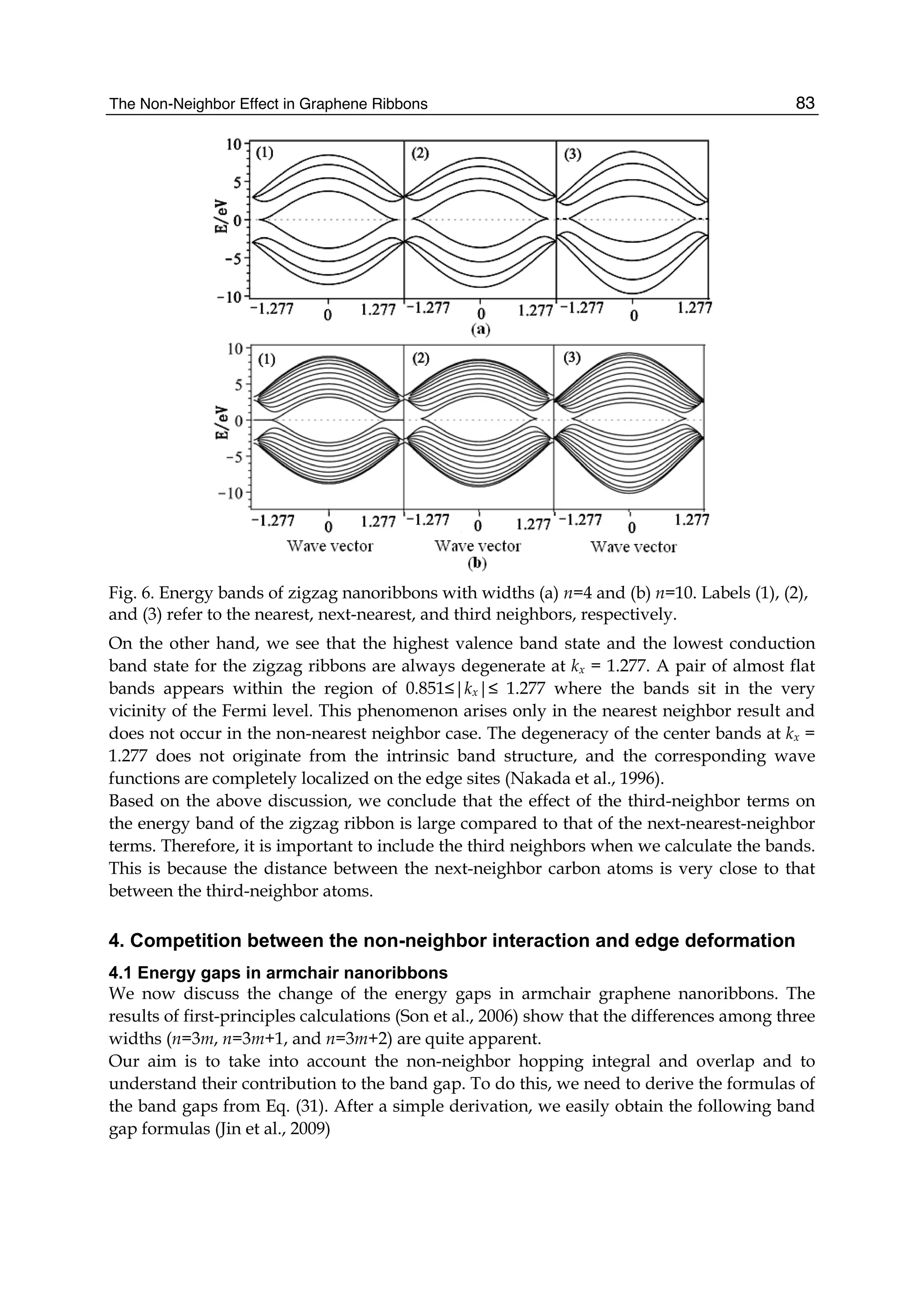
dispersion relations (or energy bands) of zigzag nanoribbons are shown in Fig. 6.
In order to conveniently compare with the third-neighbor result, we also give the nearest-
and next-nearest-neighbor electronic energy bands together with it. In Fig. 6(a) and (b), the
left is the nearest-neighbor result, the middle is the next-nearest-neighbor, and the right is
the third-neighbor for the ribbon widths n=4 and n=10. We see from Fig.6 that the zigzag
graphene nanoribbons are metallic and the energy bands are wide (more than 10eV), and
the spacing between the energy bands is decreased as increasing of the width n. When the
nearest neighbor interaction is taken only into account, the energy band structure is
symmetrical (see Fig.6 (1)). But the next-nearest-neighbor hopping and overlap can make the
energy bands become nonsymmetrical, i.e. the conduction band becomes narrowed and the
valence band is widened. It is obvious that the top of the conduction band is pressed
downward and the bottom of the valence band is pulled downward. However, the effect of
the third neighbors on the band structure is the same as that of the next-nearest neighbors,
but the latter is stronger than the former.](https://image.slidesharecdn.com/grrphysicsandapplicationsofgraphene-theory-140422181144-phpapp02/75/physics-and_applications_of_graphene_-_theory-92-2048.jpg)

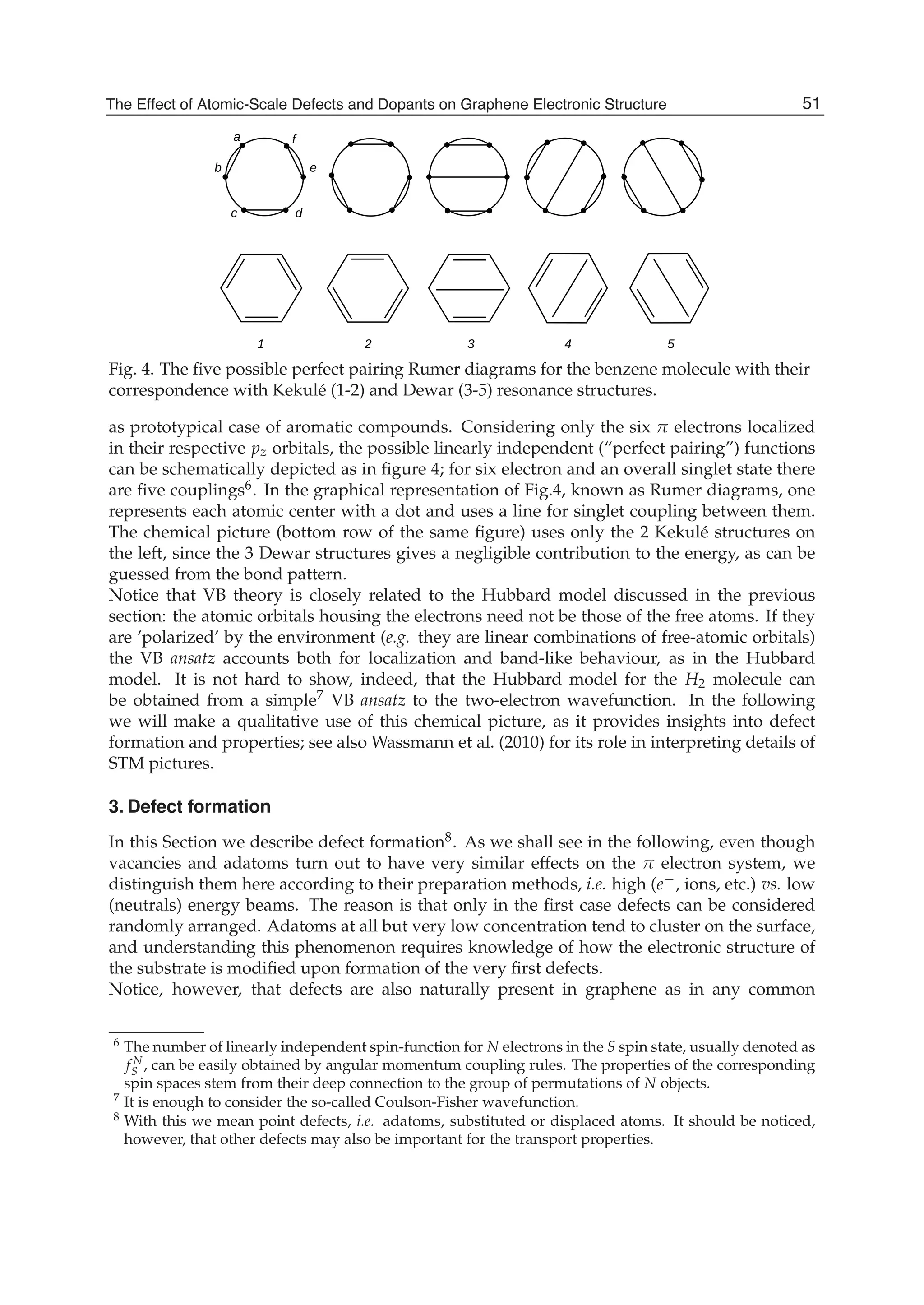
![Although the interaction between electrons is well known, the facts that electrons, with a spin
quantum number of 1/2, have to obey specific statistical rules and that one normally has to
deal with quite a few of them at the same time make this problem immensely formidable. One
approach that has become the standard one for large-scale electronic simulations is the density
functional theory in the so-called Kohn-Sham framework. It is based on a theorem stating that
the ground-state energy of a many-electron system can be represented as a functional of the
electron density only. As a result, one can obtain the electronic energy without dealing with
the many-body wave function which is highly multidimensional with the notorious property
of being antisymmetric with respect to particle exchange. Being a scalar in the real space,
the electron density is a much simpler quantity to manage, making it possible to investigate
more complex systems. By minimizing the energy functional with respect to possible density
distributions one can then determine the ground-state electronic energy for a given atomic
arrangement.
The energy minimization procedure is most conveniently carried out by a mapping of the
truly interacting system to an auxiliary system of noninteracting particles with the same
density distribution. The resulting total-energy functional
E[n] = T0[n] + d3
r vext(r) n(r) + Eh[n] + Exc[n] (1)
includes the kinetic energy functional of the noninteracting system T0[n], external potential
energy, Hartree energy Eh[n], and the so-called exchange-correlation energy functional Exc[n].
Exc[n] includes all the many-body effect as well as the difference in the kinetic energies of the
interacting and noninteracting systems.
The direct variation of energy with respect to the density is replaced by finding the
noninteracting orbitals self-consistently in the local Kohn-Sham equations
(
¯h2
2m
2
+ Vext + Ve f f ) i = i i , (2)
where the effective one-particle potential Ve f f includes the Hartree potential and the
exchange-correlation potential derived from a functional derivative Vxc = Exc/ n. The
density is calculated from all occupied one-particle orbitals. The fact that the effective
potential is a simple local function makes a tremendous difference in practical calculations.
Other quantum-chemistry schemes such as the Hartree-Fock method commonly involves
nonlocal operators which require much more computational resources. It is ok that the
density-functional theory has become the prevailing approach in modern electronic-structure
calculations with wide applications in quantum chemistry and materials physics.
Inarguably one could not have solved the exact many-body problem by regrouping energy
terms. As a matter of fact, although the existence of the exchange-correlation energy functional
Exc is fully established, its exact form remains unknown and contains integrals of nonlocal
quantities. It is therefore a challenging many-body problem to investigate this important
quantity in real materials. In practical calculations, approximations to the energy functional
Exc are required. Commonly used ones include the local-density approximation (LDA), in
which the density is assumed to be locally uniform and the result for a homogeneous
electron gas is used point by point based on the local density, and the generalized gradient
approximation (GGA), in which the gradient correction to the LDA is added.
In order to study systems of hundreds of atoms, one focuses on the properties of the
valence electrons and employ norm-conserving pseudopotentials to model the effects of core
electrons. The one-particle orbitals will be expanded in terms of plane waves to eliminate
117Structural and Electronic Properties of Hydrogenated Graphene](https://image.slidesharecdn.com/grrphysicsandapplicationsofgraphene-theory-140422181144-phpapp02/75/physics-and_applications_of_graphene_-_theory-127-2048.jpg)
![in which the matrix elements G ( n, k, p) are defined as the Fourier transforms of
G (k, p, ) = T ˆ†
k ( ) ˆp(0) with a, = a, b. k and p denotes the electronic wavevectors
is the complex time variable and n are the fermionic Matsubara frequencies.
The system Green’s function (Eq. 2) can be solved from the equations-of-motion derived
based on Hamiltonian (Eq. 1). The rationale behind the solution procedure is to seek for the
relationship behind G ( n, k, p) and G0( n, k). the Matsubara Green’s function for pristine
graphene, where the later can be expressed analytically as (Peres et al., 2006):
G0
( n, k) =
G0
aa( n, k) G0
ab( n, k)
G0
ba( n, k) G0
bb( n, k)
=
j= 1
1/2
i n j (k)
1 jei (k)
je i (k) 1
, (3)
with ei (k) = (k)/ (k) .
Since we are interested in the electronic DOS on the impurity (A) site and its
nearest-neighboring (B) sites, therefore, it would be sufficient to solve for Gaa( n, k, p) and
Gbb( n, k, p) in Eq. 2. The electronic DOS can then be found from the imaginary parts of
the retarded Green’s functions Gr
aa( , k, p) and Gr
bb( , k, p) through analytical continuation of
the Matsubara Green’s functions. The presence of both diagonal and nondiagonal disorders
means that the solutions will be of a more complex form than the usual T-matrix for a single
Anderson impurity scattering problem, and the results are
Gaa( n, k, p) = k,pG0
aa( n, k) + g( n) + h( n) G0
aa( n, k) + G0
aa( , p)
+ Gaa( n, k)T( n)G0
aa( n, p), (4)
Gbb( n, k, p) = k,pG0
bb( n, k) +
t2 (k) (p)
(i )2
G0
bb( n, k)T( n)G0
bb( n, p), (5)
where
g( n) = t2
0
¯G0
aa( n)/[NcD( n)], (6)
h( n) = t0(t t0)/[NcD( 0)], (7)
and
T( n) = [i nt0(2t t0) 0t2
]/[NcD( n)], (8)
with
D( n) = (t t0)2
+ i nt0(t t0) 0t2 ¯G0
aa( n), (9)
and
¯G0
aa( n) =
1
Nc k
G0
aa( n, k). (10)
The important term is the g( n whose double Fourier transform gives Gaa( n, 0, 0) which is
the return (back-scattering) amplitude of the electron wave to the impurity site. Its magnitude,
which depends on D( n) , depicts the electronic DOS on the impurity sites.
In the case of Al doping, where the dopant has a larger atomic radius than carbon, we can let
t0 = t, with 0 0, as a limiting case. This gives,
g1( n) =
¯G0( n)
(4 4i n ¯G0( n)) + (i n 0
¯G0( n))
. (11)
136 Physics and Applications of Graphene - Theory](https://image.slidesharecdn.com/grrphysicsandapplicationsofgraphene-theory-140422181144-phpapp02/75/physics-and_applications_of_graphene_-_theory-146-2048.jpg)
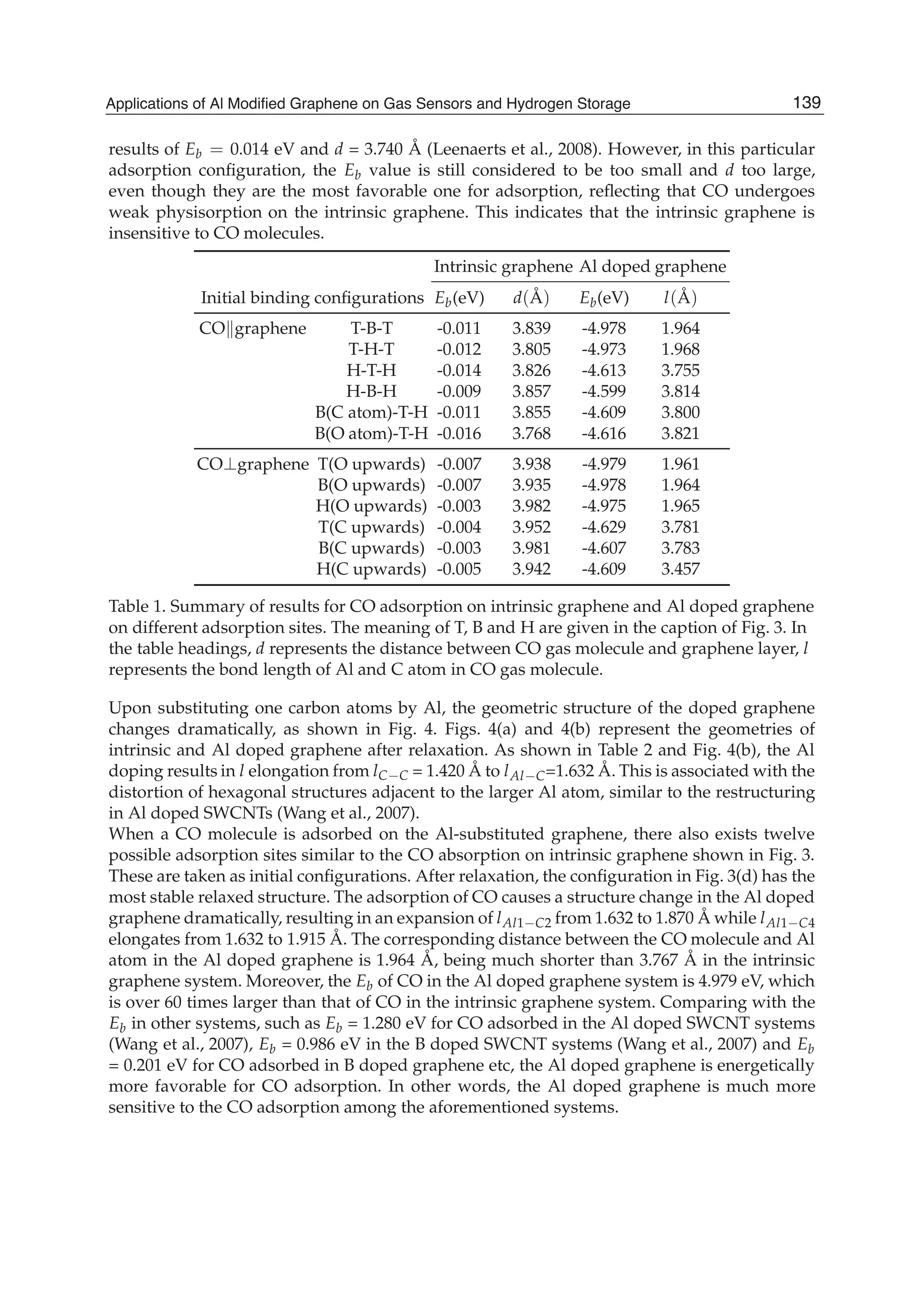
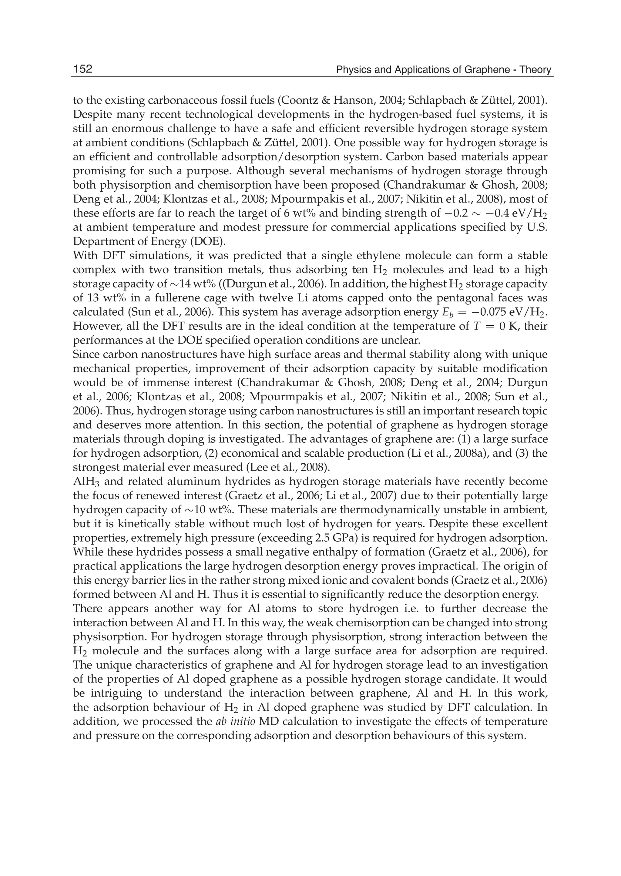
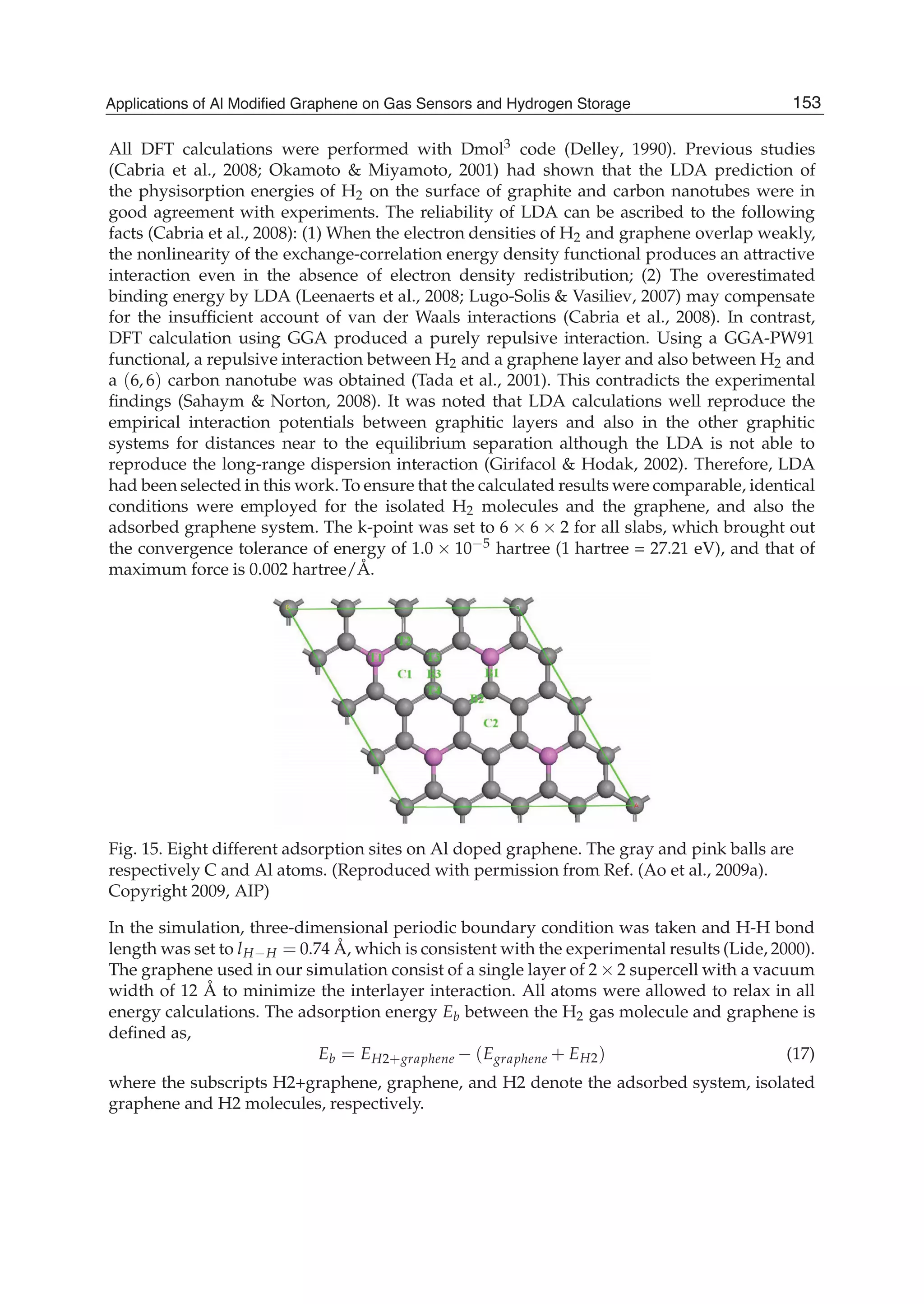
![System Configuration Bond Bond length l (Å) Q (e)
Intrinsic graphene Fig. 4(a) C1-C2 1.420
C1-C3 1.420
C1-C4 1.420
Fig. 4(c) C1-C2 1.420 0.003
C1-C3 1.421
C1-C4 1.421
Al doped graphene Fig. 4(b) Al1-C2 1.632
Al1-C3 1.632
Al1-C4 1.632
Fig. 4(d) Al1-C2 1.870 0.027
Al1-C3 1.910
Al1-C4 1.915
Table 2. Some structure parameters of intrinsic graphene and Al doped graphene before and
after adsorption of CO molecule. Q denotes electrons transferred from the graphene layer to
CO molecule, measured in the electronic charge e.
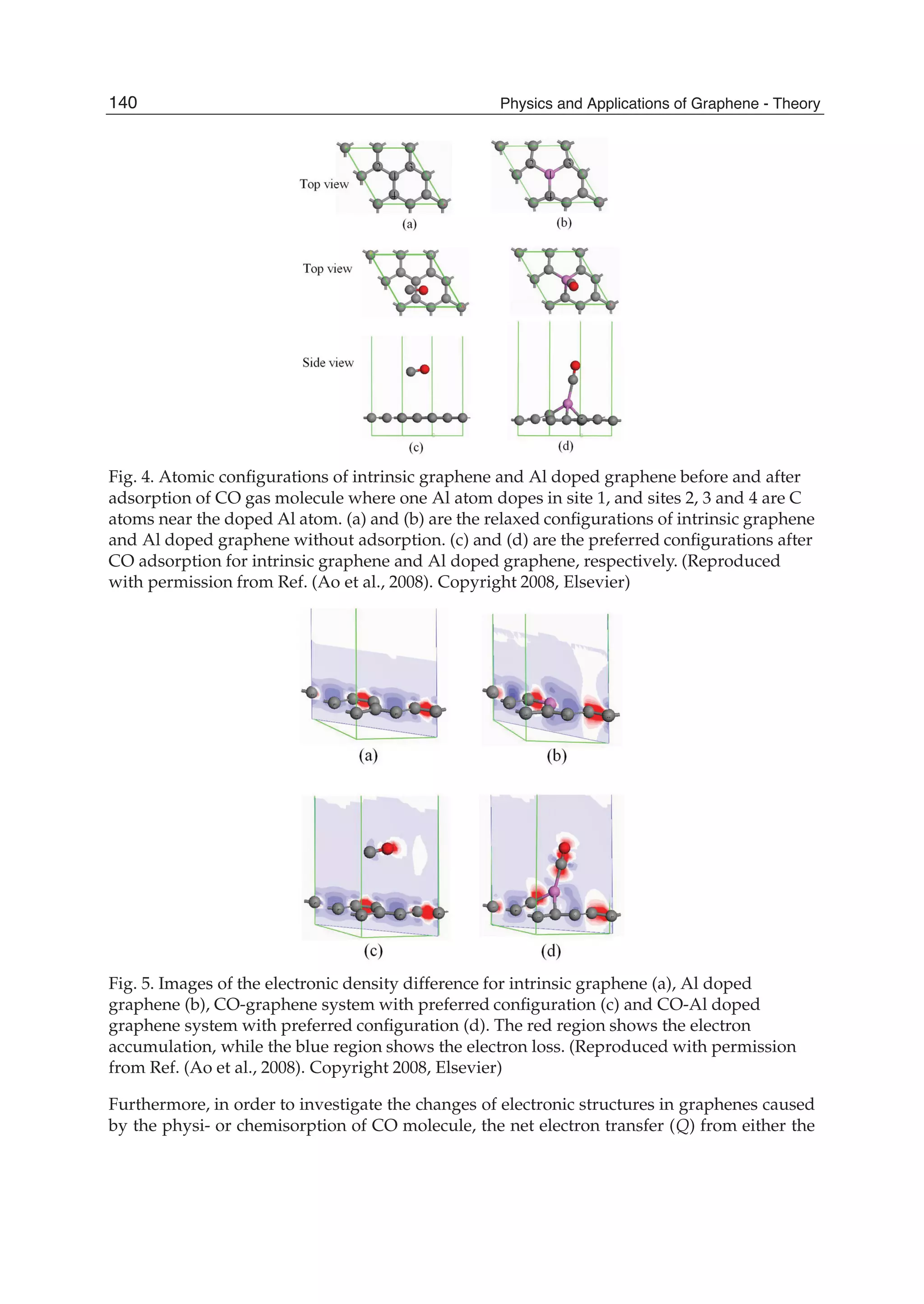
intrinsic or the Al doped graphene to the polar CO molecules had been calculated by Mulliken
analysis, where Q is defined as the charge variation caused by the CO absorption. As listed
in Table 2, Q = 0.027 e in the Al doped graphene is almost an order of magnitude larger
than 0.003 e in the intrinsic graphene. This supports the notion that the Al doping influences
the electronic properties of graphene substantially. This can also be verified by the difference
of electronic densities between the intrinsic and Al doped graphenes with and without the
CO adsorption as shown in Fig. 5. In the figure, the red and blue regions represent the areas
of electron accumulation and the electron loss, respectively. Fig. 5(a) indicates the bond in the
intrinsic graphene is of covalent nature because the preferential electron accumulation sites are
mainly located within the bond rather than heavily centered on a particular atom. However,
the electron density distribution along the covalent Al-C bonds has been significantly altered
due to the difference in electron affinity of Al and C atom [Fig. 5(b)]. Physisorption of
CO on the intrinsic graphene does not alter the electron distribution for both CO molecule
and graphene, implying the weak bonding characteristics. It is discernable that electronic
polarization is induced by the preferential accumulation of electrons on O in CO molecules
[Fig. 5(c)]. As distinct from the CO absorption on the intrinsic graphene, the chemisorption
of CO on Al doped graphene leads to significant electron transfer from the graphene to CO
molecule [Fig. 5(d)]. In this case, the electrons not only accumulate on the O atom but also
on the C atom of the molecule bond with the doped Al atom. The final position of Al atom
in the chemisorbed CO-Al-graphene complex is thus a direct consequence of the maximized
degree of sp3 orbital hybridization with neighboring C atoms from both the graphene layer
and CO molecule. This is evidential because the red lobes around C atoms in Fig. 5(d) are both
pointing towards Al atom.
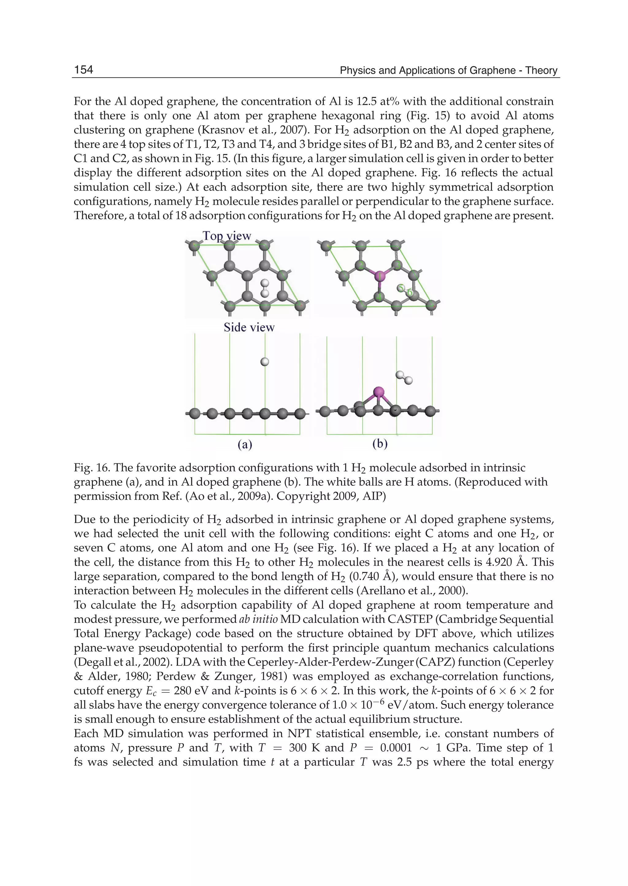
To further determine the effects of CO absorption on electrical conductivity, DOS for the both
systems with and without the absorption were calculated. As shown in Figs. 6(a) and (b), the
Al doping in graphene enhances its electrical conductivity by shifting the highest DOS peak to
just below the Fermi level Ef , which also leads to the reduction of band gap Eg. This indicates
that the doped Al atom induces shallow acceptor states in graphene like B atom in SWCNs,
thus enhancing its extrinsic conductivity (Peng & Cho, 2003). When the CO molecule adsorbed
141Applications of Al Modified Graphene on Gas Sensors and Hydrogen Storage](https://image.slidesharecdn.com/grrphysicsandapplicationsofgraphene-theory-140422181144-phpapp02/75/physics-and_applications_of_graphene_-_theory-151-2048.jpg)
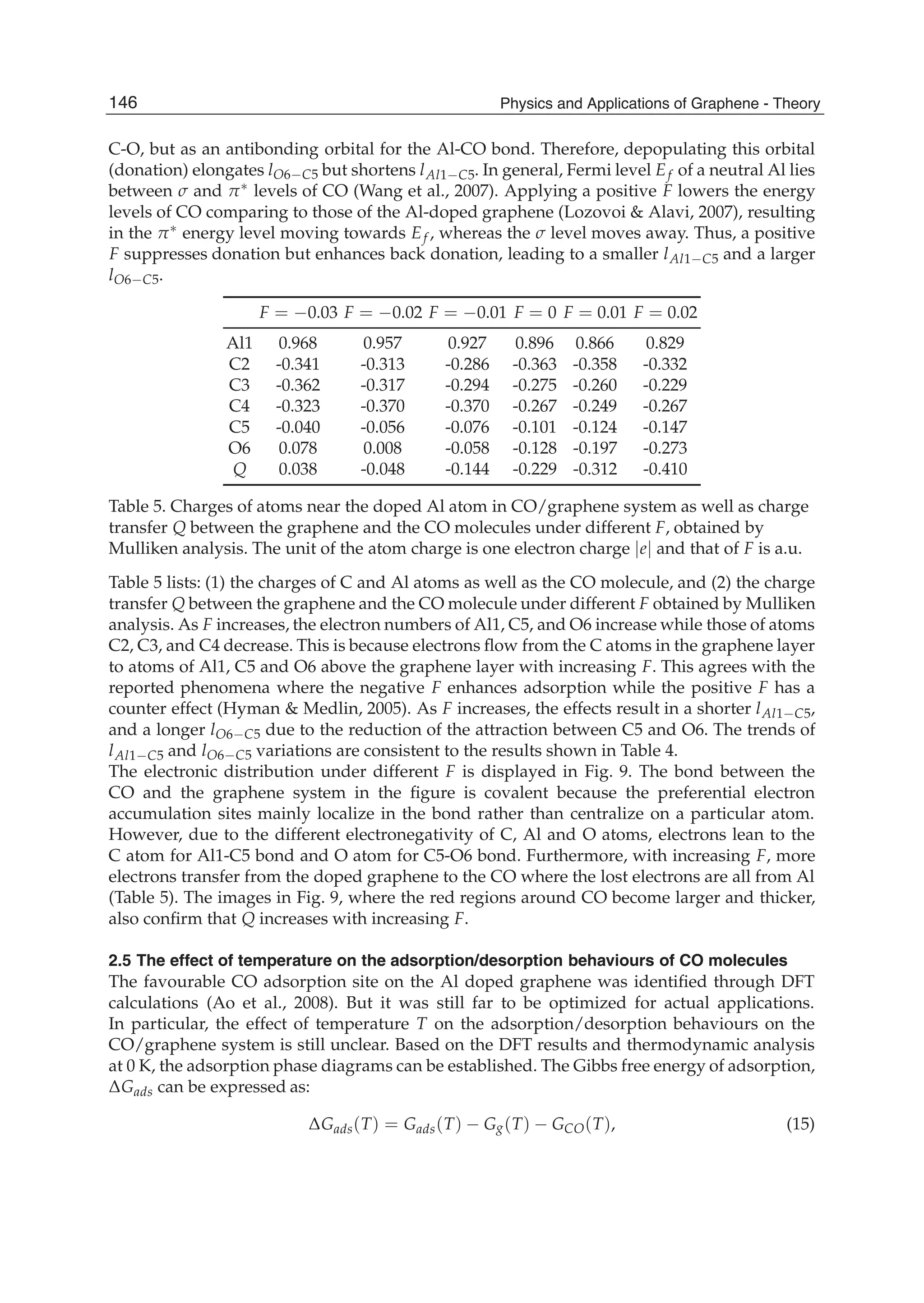
![on the intrinsic and doped graphene surfaces, the total DOSs are shown in Figs. 6(c) and 6(d).
In the intrinsic graphene, the DOS of CO-graphene system near Ef have no distinct change,
and the conductivity change is barely observable. It implies that the intrinsic graphene would
not be an ideal CO gas sensor. However, for the Al doped graphene with the most stable
chemisorbed CO configuration [Fig. 6(d)], not only the highest DOS peak shifts over the Ef ,
but also the DOS value increases dramatically. This results in an Eg closure [Fig. 6(d)] where
Eg of the Al doped graphene is 0.18 eV without adsorption and the Eg becomes zero with
adsorption. It suggests that extra number of shallow acceptor states have been introduced
when the Al doped graphene interacts with the highly polar CO molecule. As a result, the
chemisorbed CO on the Al doped graphene gives rise to a large increase in the electrical
conductivity of the doped graphene layer. By detecting the conductivity change of the Al
doped graphene systems before and after the adsorption of CO, the presence of this toxic
molecule can be detected sensitively. Therefore, the Al doped graphene is a promising sensor
material for detecting CO molecules. However, desorption of CO molecule from the Al doped
graphene is difficult due to the strong bonding of Al-CO (Peng et al., 2004). This can be solved
by applying an electric field F to reactivate the sensor materials (Hyman & Medlin, 2005).
Fig. 6. Electronic density of state (DOS) of intrinsic graphene (a), Al doped graphene (b),
CO-graphene system with preferred configuration (c) and CO-Al doped graphene system
with preferred configuration (d).(Reproduced with permission from Ref. (Ao et al., 2008).
Copyright 2008, Elsevier)
2.4 The effect of electric field on the adsorption/desorption behaviours of CO molecules
The first theoretical work with quantum mechanical calculations on electric field F inducing
adsorption/desorption was studied for N2 molecule on Fe(111) surface (Tomanek et al., 1985).
Recent simulation works on the effects of F on: (1) the adsorption and dissociation of oxygen
on Pt(111) (Hyman & Medlin, 2005), (2) electronic structure of Au-XO(0,-1,+1) (X = C, N and
O) (Tielens et al., 2007), and (3) vibrational frequencies of CO on Pt(111) (Lozovoi & Alavi,
2007) showed that F could induce some new physical phenomena by changing their electronic
properties (McEwen et al., 2008).
Therefore, it is of interest to investigate how F influences the adsorption/desorption
behaviours of CO on Al-doped graphene. Here, the favorable adsorption configurations of
CO on Al-doped graphene under different F had been determined by DFT calculation, and
the effects of F on the corresponding interaction between CO and Al-doped graphene will
be further discussed. All DFT calculations were performed using Dmol3 code with the same
settings as above in the section 2.3 (Delley, 1990; 2000).
142 Physics and Applications of Graphene - Theory](https://image.slidesharecdn.com/grrphysicsandapplicationsofgraphene-theory-140422181144-phpapp02/75/physics-and_applications_of_graphene_-_theory-152-2048.jpg)
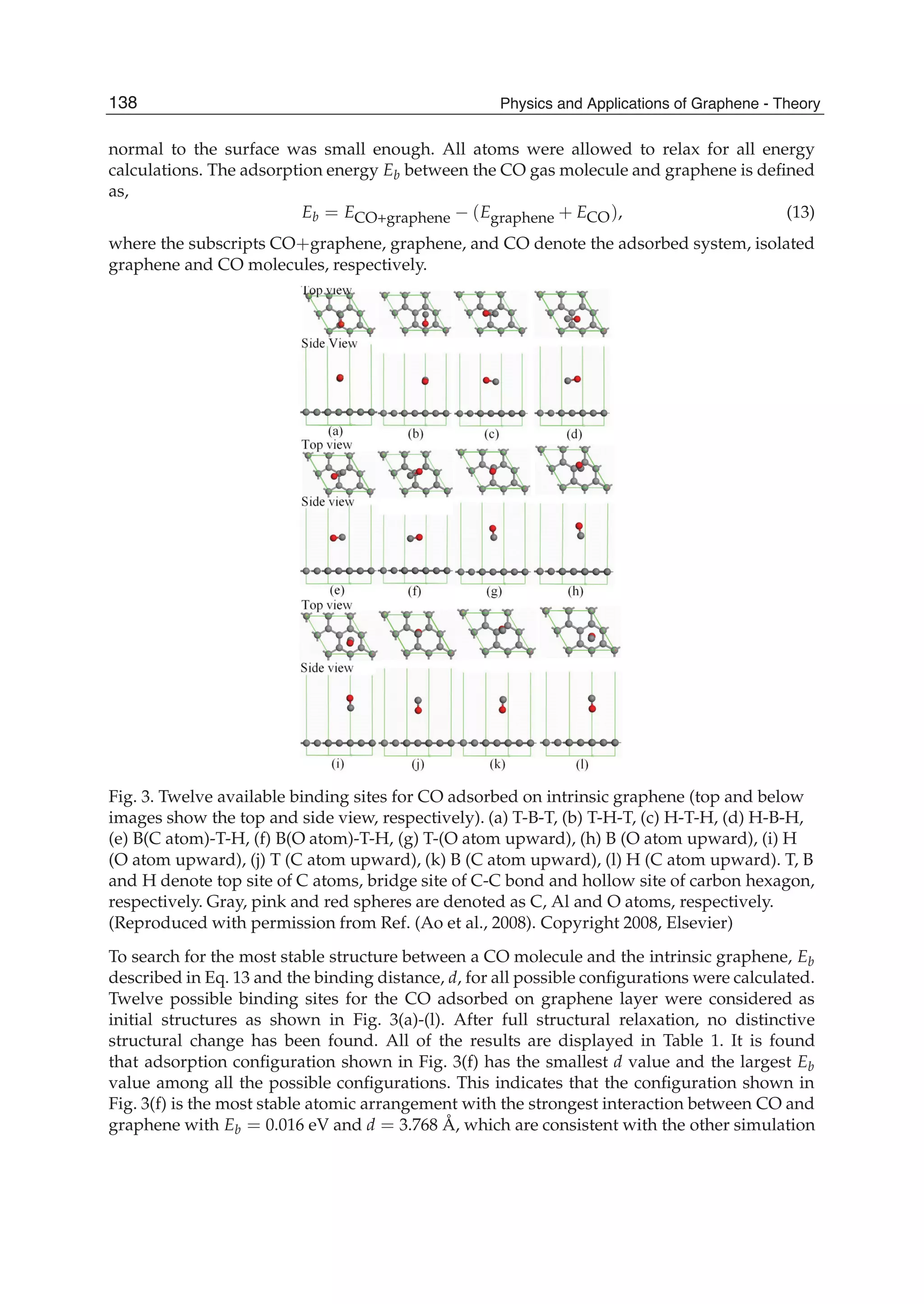
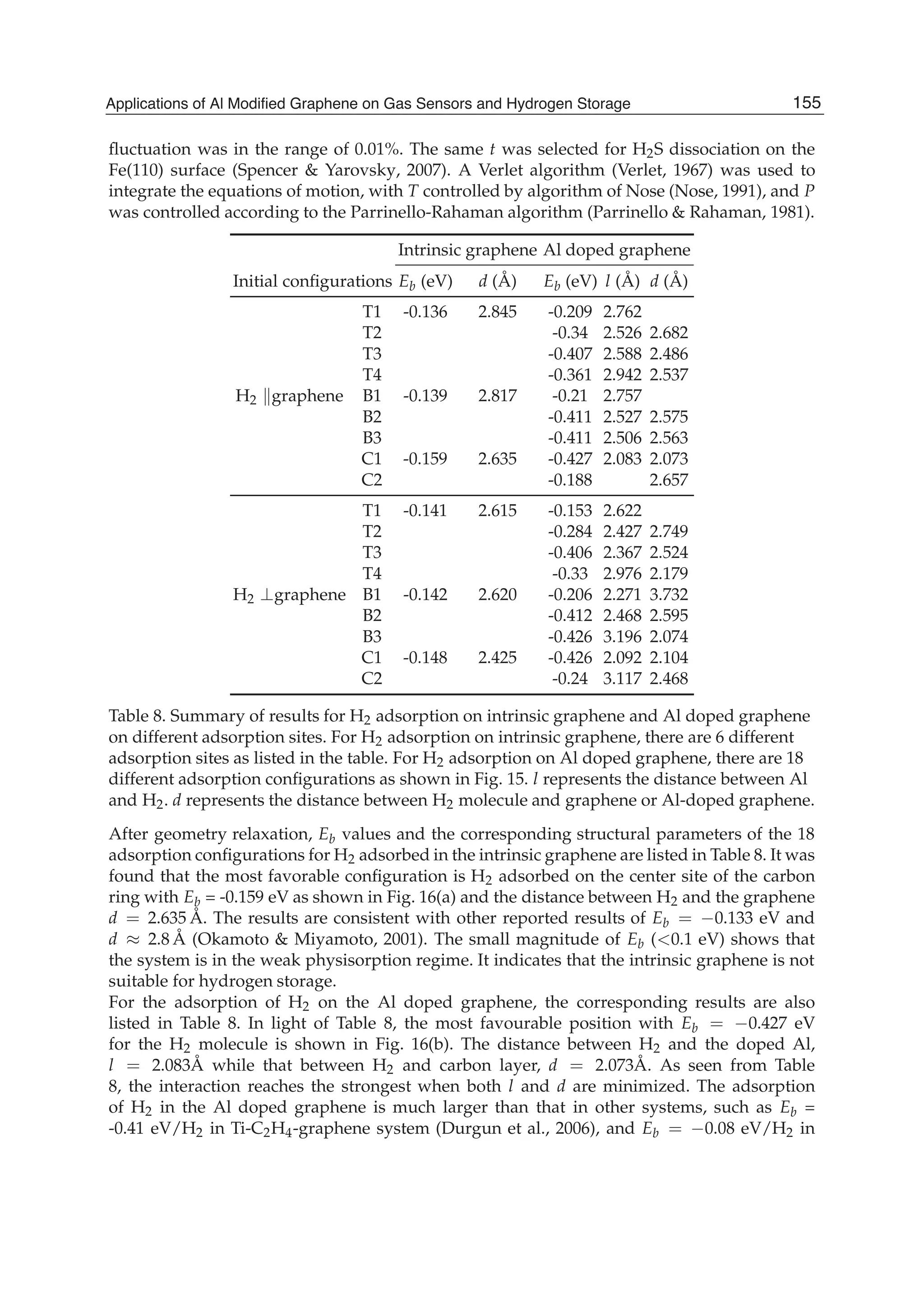
![Fig. 7. The favorite adsorption configurations under different F. Atomic structures when
F = 0.03 a.u. (a), F = 0.02 a.u. (b),F = 0.01 a.u. (c),F = 0 (d), F = 0.01 a.u. (e), F = 0.02
a.u. (f), (g) stable structure cannot be gotten when F = 0.03 a.u. and this structure is the
configuration after 200 geometry optimization steps. The direction of the positive F is
pointed out by the arrow. In the figure, gray, pink and red spheres are C, Al and O atoms,
respectively. One Al atom dopes in site 1 and sites 2, 3 and 4 are C atoms near the doped Al
atom, sites 5 and 6 are C and O atoms in the CO molecule. (Reproduced with permission
from Ref. (Ao et al., 2010a). Copyright 2010, Elsevier)
In the calculations, all atoms were allowed to relax. Al-doped graphene structures were
obtained through substituting one C atom in the graphene supercell by an Al atom as
shown in Fig. 7. In this case, the concentration of the doped Al in graphene is 12.5% atomic
ratio. For CO adsorption on Al-doped graphene, there are two highly symmetric adsorption
configurations: (1) CO molecule resides parallel to the graphene surface, and (2) CO molecule
resides perpendicular to the graphene surface. The detailed structures are similar as in the
literature [Fig. 1 in Ref. (Ao et al., 2008)]. The Eb(F) of CO molecule on Al-doped graphene
under F can be determined by (Acharya & Turner, 2007),
Eb(F) = ECO+graphene(F) [Eprot(F) + ECO(F)]. (14)
where the subscripts CO+graphene, prot, and CO denote the adsorbed system, the initial
isolated graphene with Al atom protruding from the graphene surface and the CO molecule,
respectively. In the simulation, F had been chosen in the range of -0.03 0.03 a.u. (1 a.u. = 51
V/Å) and its positive direction is pointed out by the arrow in Fig. 7. Note that the length of
the vacuum layer along the direction of normal to the graphene layer in the simulation system
is about 15 Å. Thus, the maximum voltage required to induce the electric field with intensity
of 0.03 a.u. is about 23 V, which can be easily realized in actual applications.
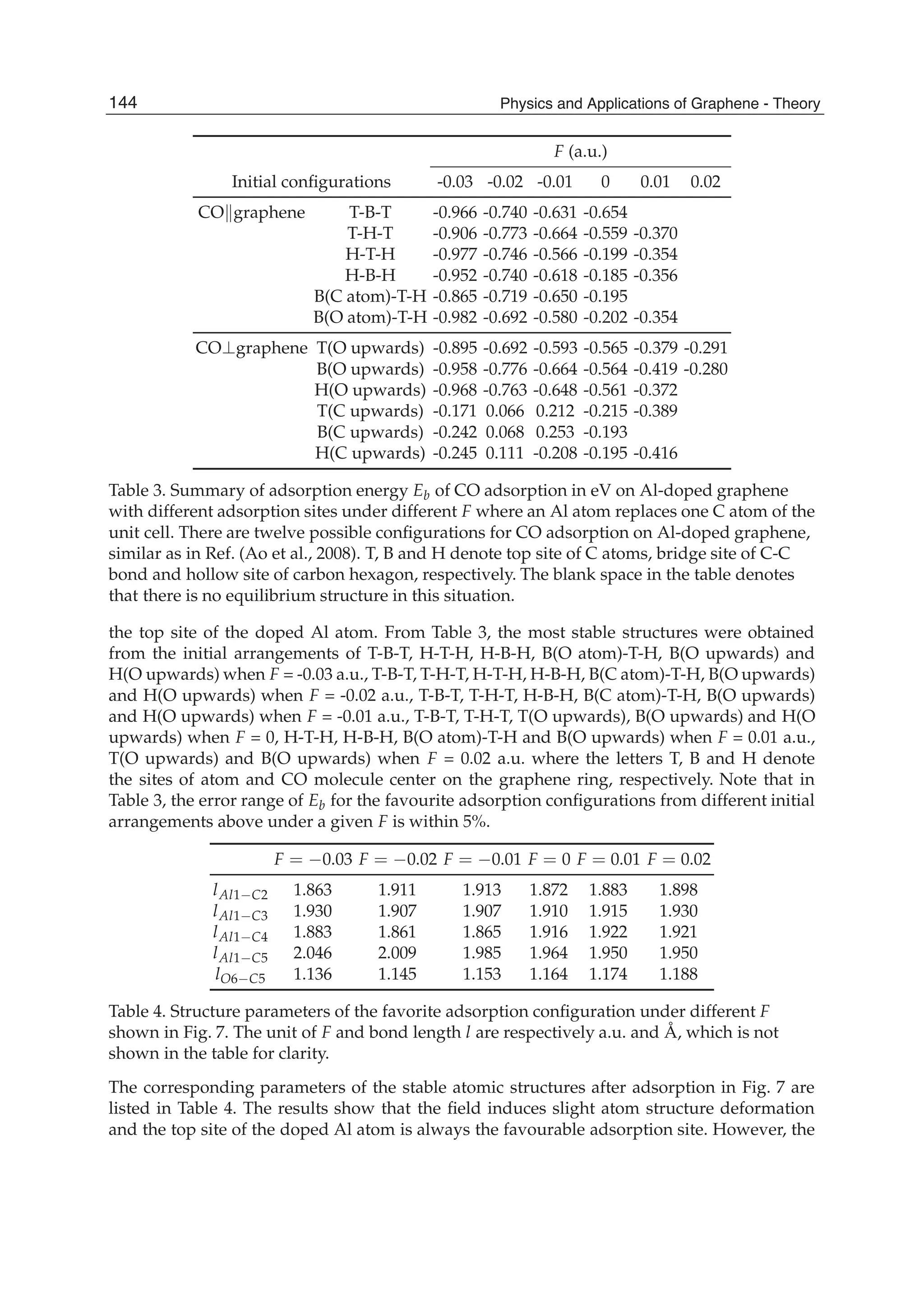
Eb of the CO/graphene systems with all possible adsorption configurations in the presence of
F is listed in Table 3. Based on the calculated Eb values, the corresponding favourite adsorption
configurations under different F are present in Fig. 7 where the CO molecule always takes
143Applications of Al Modified Graphene on Gas Sensors and Hydrogen Storage](https://image.slidesharecdn.com/grrphysicsandapplicationsofgraphene-theory-140422181144-phpapp02/75/physics-and_applications_of_graphene_-_theory-153-2048.jpg)
![a time step of 1 fs at the temperatures from 300 to 450 K with an interval of 50 K. The
simulation time t at the particular temperature was 2.5 ps where the total energy fluctuated
in the range of 0.01%. MD calculation was based on the velocity Verlet algorithm (Verlet,
1967) for integration of the equation of motion. The implemented algorithm performs the
Yoshida-Suzuki multiple-step numerical integration of varying quantity, depending on the
choice of interpolation parameters (Suzuki, 1991; Yoshida, 1990). A key parameter in the
integration algorithms is the integration time step. A common rule-of-thumb used to set the
time step is that the highest frequency vibration should be sampled between 10 and 20 times
in one cycle. In this system, the frequency is in the order of 1013 Hz, the time step was thus
set as 1 fs within a reasonable range (Seitsonen et al., 2001). The temperature was controlled
by algorithm of Nose (Nose, 1984). The thermostate employs a feedback loop between the
instantaneous kinetic energy and the set temperatures. The rate of feedback is determined by
the mass parameter, Q (Q = 2) (Loffreda, 2006; Spencer & Yarovsky, 2007; Todorova et al.,
2007).
With the thermal desorption method, T dependent desorption time (T) function can be
expressed as (Peng et al., 2004; Raaen & Ramstad, 2005)
(T) = 1
0 exp[ Eb(T)/kBT] (16)
where kB is the Boltzmann’s constant (8.62 10 5 eV/K), and 0 is the attempt frequency
of 1013 Hz for CO (Seitsonen et al., 2001). This thermal desorption method is close to the
experimental conditions and it can be used to determine the thermodynamical properties of
the adsorption systems (Raaen & Ramstad, 2005).
With the adsorption structures determined by the DFT calculations at an ideal condition, the
phase diagram of adsorption/desorption for the CO adsorbed on the Al doped graphene as
a function of temperature can be established with the atomistic thermodynamics described in
Eq. 15. Such a simple approach allows the exploration of Gads(T) in an actual condition with
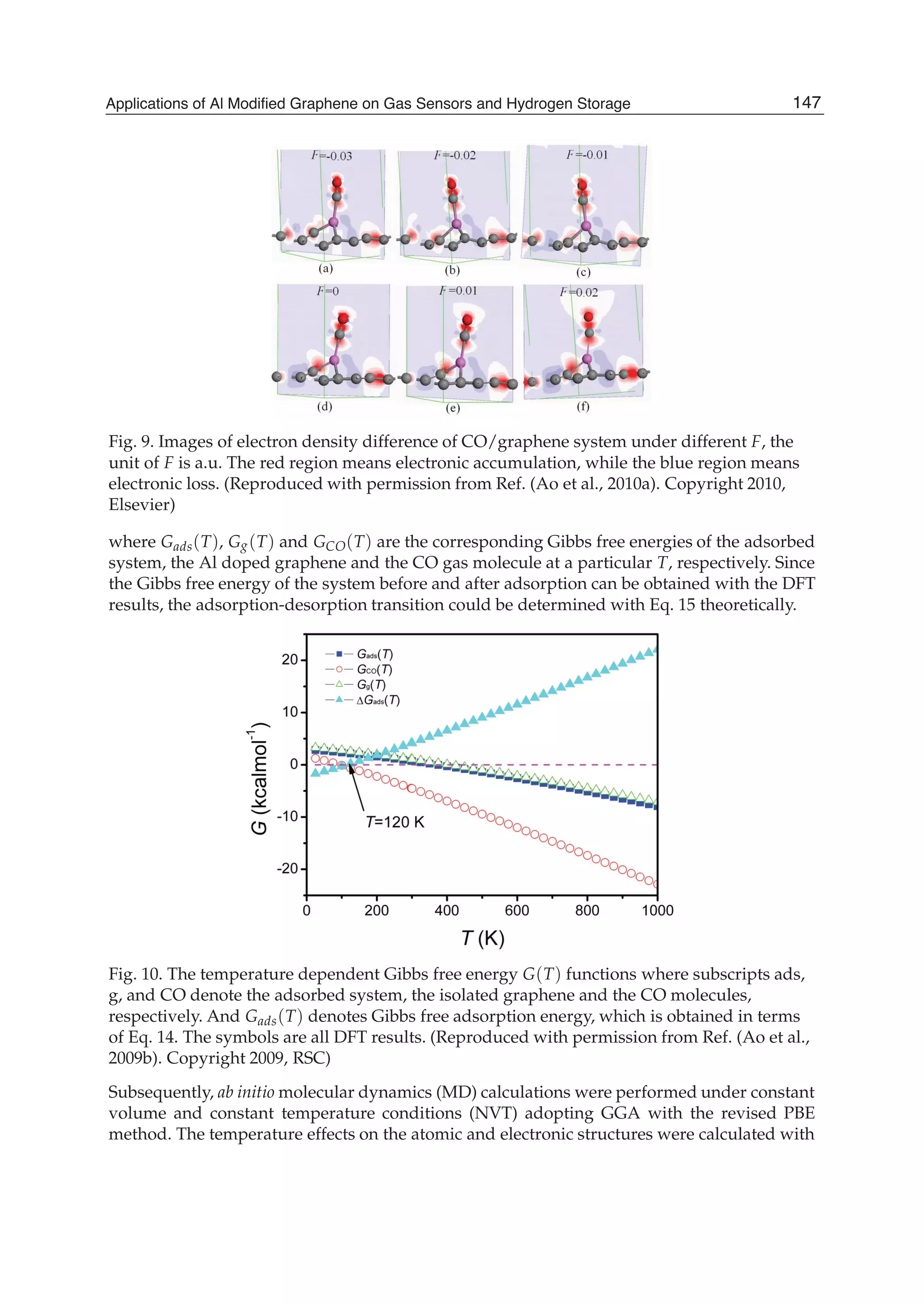
respect to experiments. Gads(T), Gads(T), Gg(T) and GCO(T) functions are plotted in Fig. 10.
The results show that Gads(T) increases as T increases, and eventually becomes positive at
Td = 120 K where Td is defined as the desorption temperature. In another word, the desorption
of CO from the Al doped graphene occurs when Td 120 K at the ideal state with .
T = 0 T = 300 K T = 400 K T = 450 K
lAl1 C2 1.872 1.880 1.946 1.973
lAl1 C3 1.910 1.961 1.972 1.993
lAl1 C4 1.916 1.923 1.929 1.989
lAl1 C5 1.964 1.982 2.097 4.590
lC5 O 1.164 1.161 1.159 1.157
Table 6. Some structure parameters of CO molecule adsorbed on Al doped graphene at
different temperature, where l is bond length in Å.
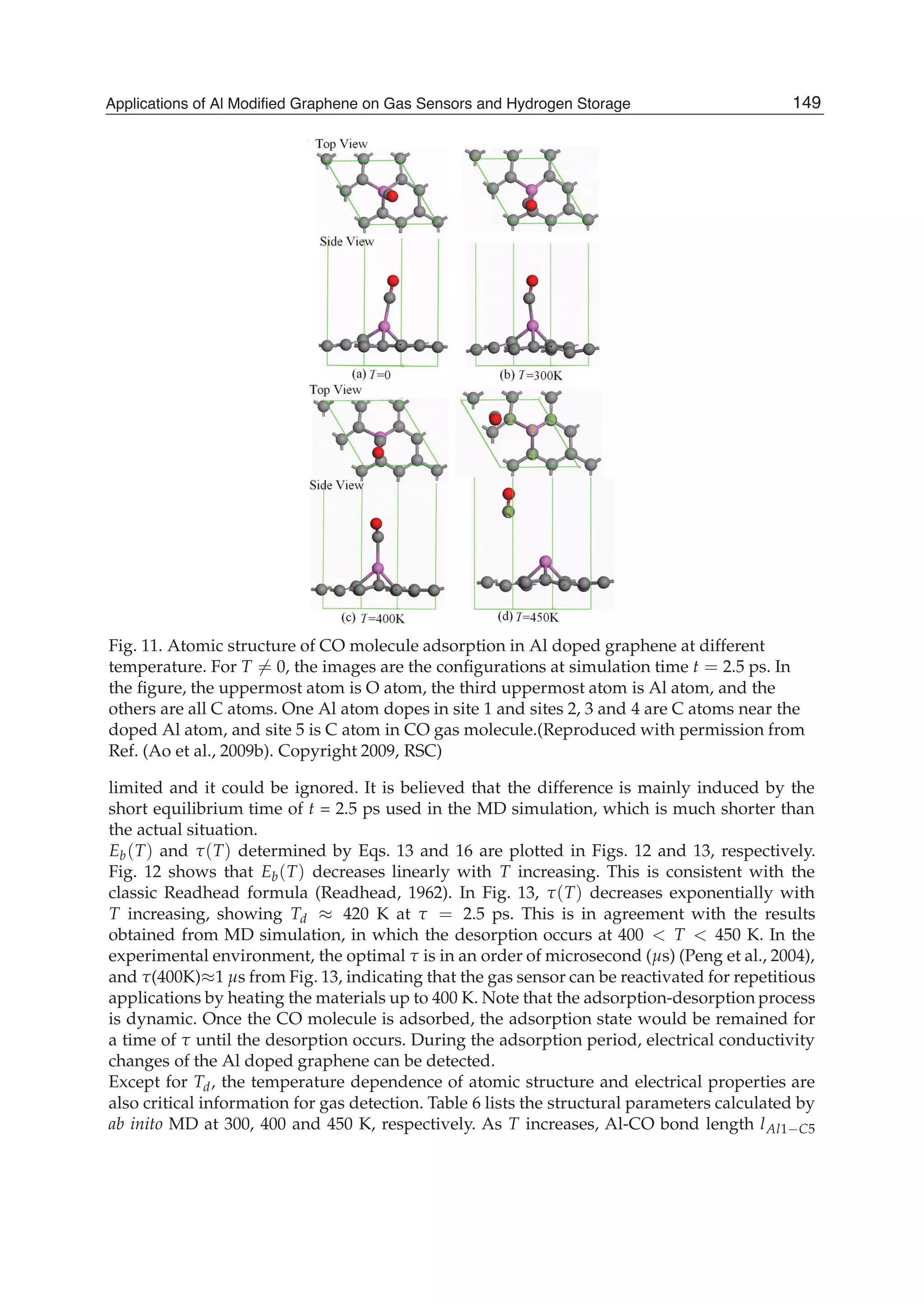
However, with ab initio MD calculation at T = 300, 350, 400 and 450 K for 2.5 ps to reach
the equilibrium at each temperature, it was found that the desorption occurred at 450 K.
The atomic configurations at the different temperatures are shown in Fig. 11 and their
corresponding atomic structural parameters are listed in Table 6. The results show that Td is
between 400 and 450 K. Since both the data for MD simulation and atomistic thermodynamics
come from the simulation, the difference of Td caused by the simulation methodologies is
148 Physics and Applications of Graphene - Theory](https://image.slidesharecdn.com/grrphysicsandapplicationsofgraphene-theory-140422181144-phpapp02/75/physics-and_applications_of_graphene_-_theory-158-2048.jpg)
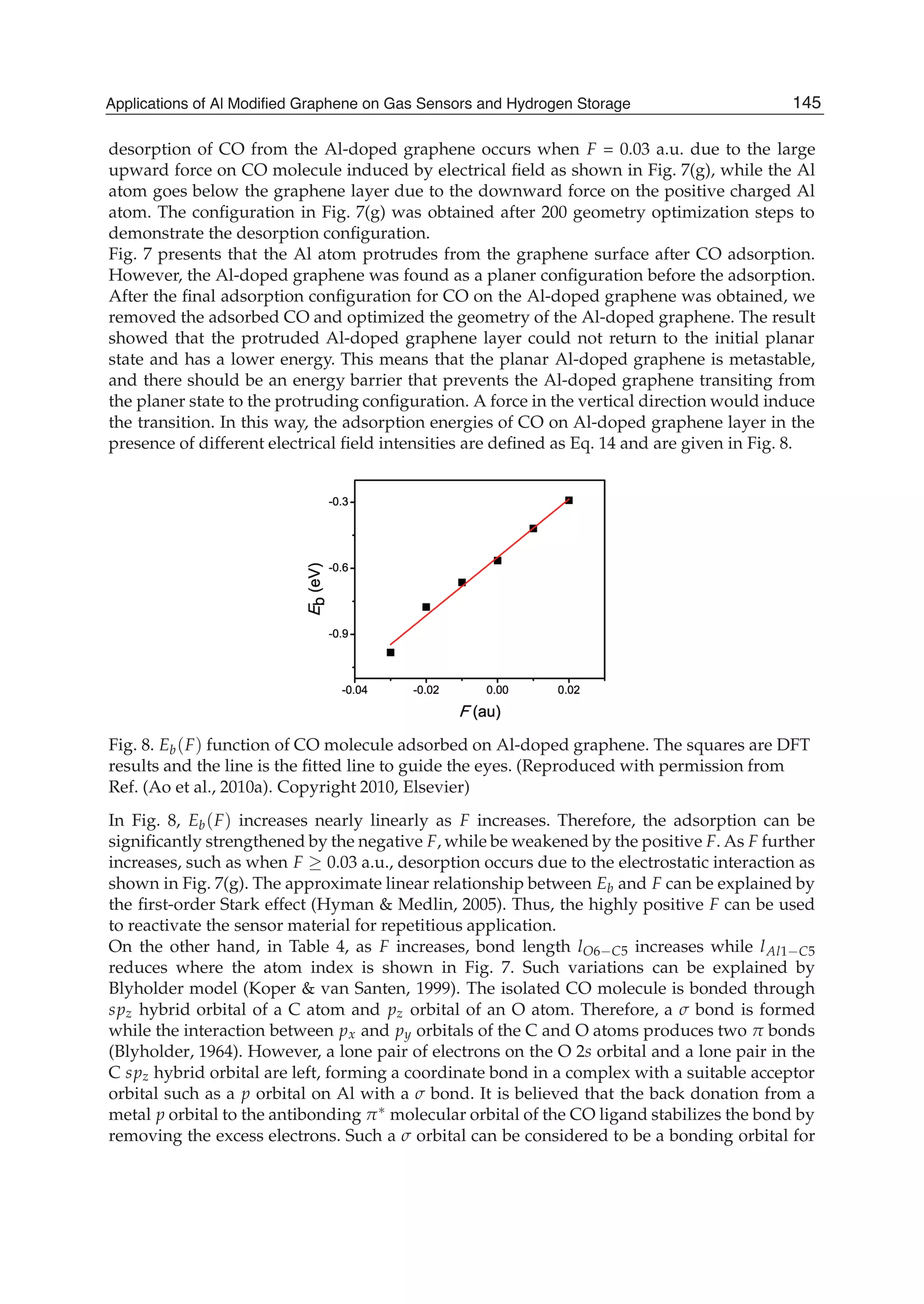
![Fig. 12. Temperature dependent adsorption energy of CO molecule in Al doped graphene
Eb(T) function. The symbol is the MD simulation result at T =0, 300, 350, 400, 450 K. The
solid line is the fitted linear function with the calculated data. (Reproduced with permission
from Ref. (Ao et al., 2009b). Copyright 2009, RSC)
Fig. 13. Temperature dependent desorption time function (T) in terms of Eq. 16 where
Eb(T) function needed is from Fig. 12. The two temperatures 398 and 420 K are
corresponding desorption temperature in MD simulation and actual situation.(Reproduced
with permission from Ref. (Ao et al., 2009b). Copyright 2009, RSC)
increases, or the corresponding bond strength decreases. This is also evidenced by the Eb(T)
declination as shown in Fig. 12. When T further increases, the desorption of CO from the Al
doped graphene occurs [Fig. 11(d)] where bond length of lAl1 C5 changes sharply from 2.097
Å at 400 K to 4.590 Å at 450 K.
In order to better understand the results, Table 7 lists the charges of C atoms surrounding the
doped Al atom, the doped Al atom and the CO molecule as well as charge transformation
Q between the doped graphene and the CO molecule, which were obtained by Mulliken
analysis. It exhibits that Q decreases as T increases and the Al atom loses electrons. The
negative charges of the C atoms surrounding the doped Al also decrease. It results in the
charge difference between the C and Al atoms decreases and the Al-C bond length in the
150 Physics and Applications of Graphene - Theory](https://image.slidesharecdn.com/grrphysicsandapplicationsofgraphene-theory-140422181144-phpapp02/75/physics-and_applications_of_graphene_-_theory-160-2048.jpg)
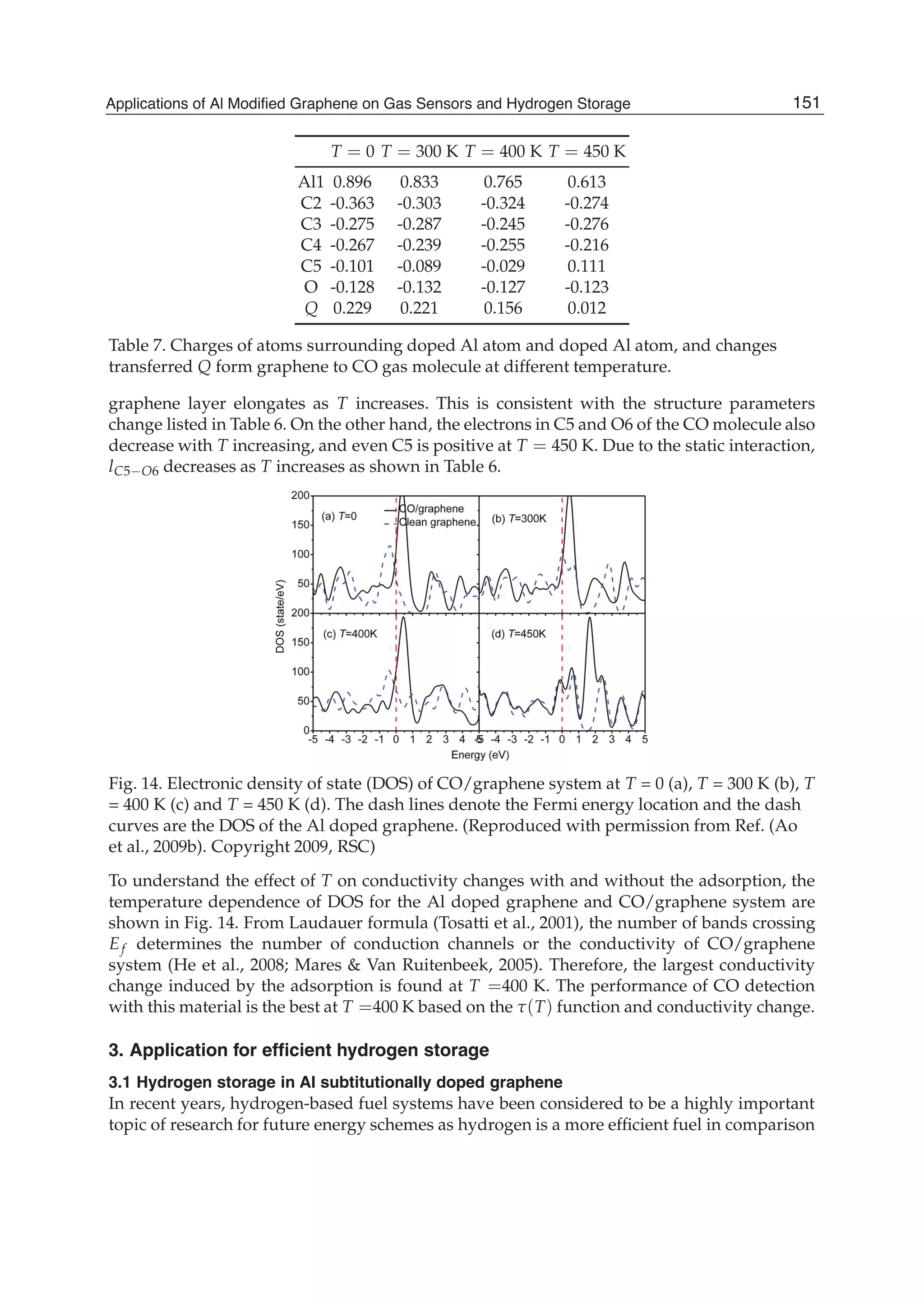
![Atom Intrinsic graphene Al doped graphene
Al1(C1) 0.001 0.292
C2 -0.002 -0.228
C3 0 -0.193
C4 0 -0.193
H5 -0.001 -0.001
H6 -0.001 0.021
Q -0.002 0.019
Table 9. Charges of atoms in H2 adsorbed in graphene system as well as charge transfer Q
between graphene and H2 molecule, obtained by Mulliken analyse. The unit of the atom
charge is one electron charge e, which is elided here for clarity.
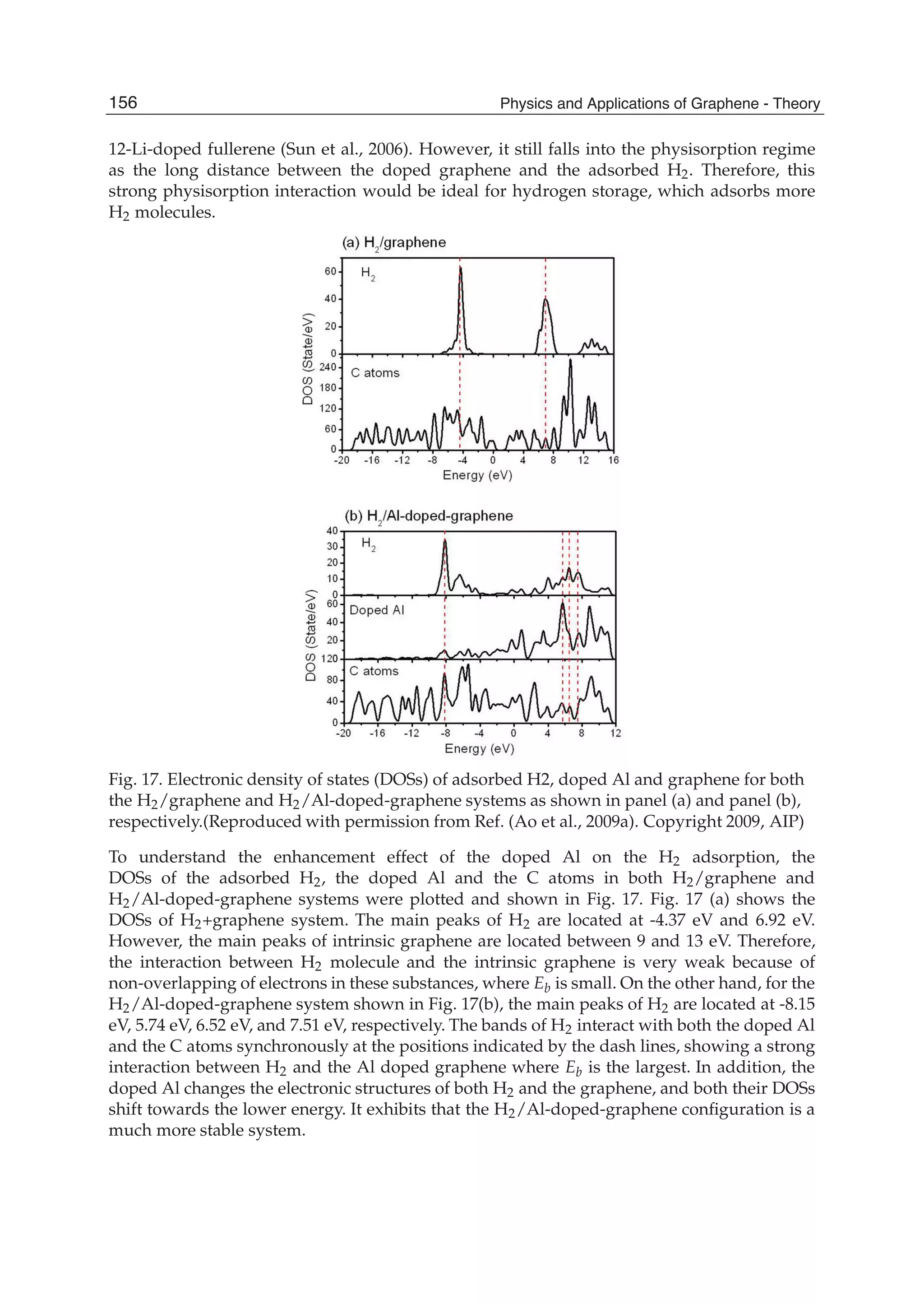
Table 9 shows the charge distribution in both the H2/graphene and H2/Al-doped-graphene
systems using Mulliken analysis. Before and after H2 adsorption, the charge variation for the
former is little while it is significant for the latter. In addition, H6 has much more positive
charge than H5. Thus, the interaction between H2 and the Al doped graphene is mainly
achieved through H6. The interaction between the band at the location of the highest peak
of DOS plot of H2 and that of C atoms implies a strong interaction between the H2 and C
atoms, as shown in Fig. 17(b).
Fig. 18. Electron density distributions in the H2/graphene [panel (a)] and H2/Al-doped-
graphene [panel (b)] systems. (Reproduced with permission from Ref. (Ao et al., 2009a).
Copyright 2009, AIP)
The illustrations of electron density distribution for the H2/graphene and
H2/Al-doped-graphene systems are shown in Fig. 18. In the system of H2/graphene
[Fig. 18(a)], no electron exists in the region between H2 and C layer while some electrons
appear in the region among H2, Al atom and C layer in the system of H2/Al-doped-graphene
[Fig. 18(b)]. This supports the notion that the H2/Al-doped-graphene possesses a much
stronger H2 adsorption ability.
After understanding the mechanism of the enhancement for H2 adsorption in the Al doped
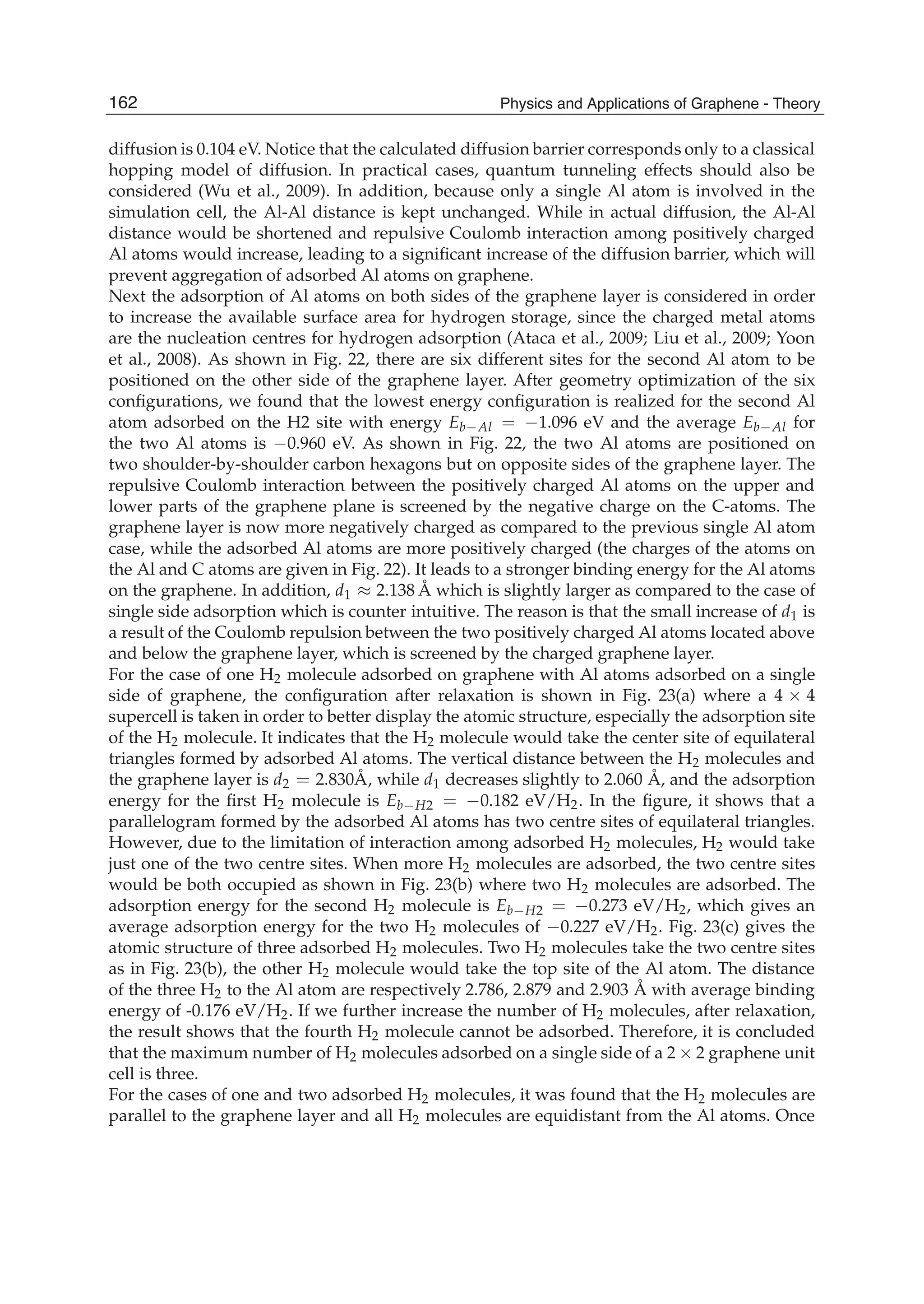
graphene, it is important to determine how much H2 molecules can be adsorbed on the 2 2
layer surface. We constructed an adsorption configuration with 3 H2 molecules adsorbed
in the three favourable C1 adsorption positions on the topside of the doped system. After
geometry relaxation, the atomic structure is shown in Fig. 19(a). It has Eb = 0.303 eV/H2,
which satisfies the requirement of Eb = 0.20 0.40 eV/H2 at room temperature
(Chandrakumar & Ghosh, 2008; Deng et al., 2004; Klontzas et al., 2008; Mpourmpakis et al.,
157Applications of Al Modified Graphene on Gas Sensors and Hydrogen Storage](https://image.slidesharecdn.com/grrphysicsandapplicationsofgraphene-theory-140422181144-phpapp02/75/physics-and_applications_of_graphene_-_theory-167-2048.jpg)
![Fig. 19. Atomic configurations H2/Al-doped-graphene system at different temperature and
pressure. (a) In the ideal condition with T = 0 K, (b) in the condition with T = 300 K and
P =0.1 GPa, (c) in the condition with T =300 K and P =0.0001 GPa, and (d) in the condition
with T =300 K and P =1 GPa. (Reproduced with permission from Ref. (Ao et al., 2009a).
Copyright 2009, AIP)
2007) set by DOE although the value of 5.1 wt% of H2 adsorbed is slightly below the DOE’s 6
wt% target.
In order to understand the effect of the adsorbed H2 molecule number on the Eb, the
configuration with 6 H2 molecules adsorbed in the Al doped graphene in the favorable C1
adsorption positions on both sides was calculated. It is found that Eb = 0.164 eV/H2, which
is almost half of the Eb for above the case where the Al doped graphene adsorbed 3 H2 on one
side of graphene. In addition, the adsorption with 8 H2 molecules in the Al doped graphene
was also calculated, and it is found 2 H2 molecules were released. In the other words, the
interaction between H2 molecules would weaken the adsorption on the doped graphene and
the saturated number of H2 molecules adsorption is 6. Note that Eb for the cases of 3 H2 and 6
H2 are respectively -0.303 eV/H2 and -0.164 eV/H2, which is about twice for the case of 3 H2
comparing with the case of 6 H2. This is because H2 molecules were very weakly adsorbed
below the graphene layer where the doped Al atom locates above the graphene layer.
It is well known that T and P have essential effects on hydrogen storage, where increasing
P and decreasing T enhance the capacity of hydrogen storage. Thus, most studied systems
are either under high P or at very low T (Sahaym & Norton, 2008), which may not be viable
for mobile applications. For example, a storage capacity of 8 wt% for purified single wall
carbon nanotubes (SWNTs) at 80 K with a hydrogen pressure of 13 Mpa (Ye et al., 1999) and
a lower hydrogen storage capacity of 2.3 wt% at 77 K were reported (Panella et al., 2005).
The hydrogen storage capacities in other carbon related materials, such as activated carbon
(AC), single walled carbon nanohorn, SWNTs, and graphite nanofibers (GNFs) were also
investigated (Xu et al., 2007). Although the AC had a capacity of 5.7 wt% at 77 K with P = 3
MPa, its capacity is 1% at 300 K (Xu et al., 2007). Recent experimental results demonstrated
that the intrinsic graphene has hydrogen storage capacity of 1.7 wt% under 1 atm at 77 K, and
3 wt% under 100 atm at 298 K (Ghosh et al., 2008). Thus, to meet the DOE target, it is necessary
to study the adsorption and desorption behaviours of H2 in the Al doped graphene at T = 300
K with different P. Therefore, the adsorption behaviours of 3H2/Al-doped-graphene and
6H2/Al-doped- graphene systems were calculated under 0.0001, 0.01, 0.1 and 1 GPa using
ab initio MD simulation. For both the 3H2/Al-doped-graphene and 6H2/Al-doped- graphene
systems, we found that all H2 molecules were released at 0.0001 GPa [Fig. 19(c)]. However,
there was only one H2 molecule adsorbed in both the systems at 0.01 GPa, while the structure
158 Physics and Applications of Graphene - Theory](https://image.slidesharecdn.com/grrphysicsandapplicationsofgraphene-theory-140422181144-phpapp02/75/physics-and_applications_of_graphene_-_theory-168-2048.jpg)
![of the doped graphene was completely destroyed with H and Al forming covalent bond at 1
GPa [Fig. 19(d)]. When P = 0.1 GPa, there are three H2 left on the top side of the two Al doped
systems [Fig. 19(b)]. Therefore, the Al doped graphene for hydrogen storage capacity at room
temperature and 0.1 GPa is 5.13 wt% with Eb = 0.260 eV/H2, satisfying the requirements of
actual application. In addition, all the adsorbed H2 molecules can be released when P = 0.0001
GPa.
3.2 Hydrogen storage in graphene with Al atom adsorption
Very recently, based on DFT calculations, Ca atoms adsorbed on graphene layers and
fullerenes were found to result in high-capacity hydrogen storage mediums, which could
be recycled at room temperature (Ataca et al., 2009; Yoon et al., 2008). In these systems, the
adsorbed Ca atoms become positively charged and the semimetallic graphene changes into
a metallic state, while the hydrogen storage capacity (HSC) can be up to 8.4 wt %. However,
a recent report claimed that DFT calculations overestimated significantly the binding energy
between the H2 molecules and the Ca+1 cation centers (Cha et al., 2009). On the other hand,
Al-doped graphene where one Al atom replaces one C atom of a graphene layer was reported
as a promising hydrogen storage material at room temperature with HSC of 5.13 wt % (Ao
et al., 2009a).
In this work, DFT was applied for studying the hydrogen adsorption on graphene with Al
atom adsorption. The favourite adsorption configuration of Al atoms on single side and on
both sides of a graphene layer have been determined. The obtained materials were studied
for adsorption of H2 molecules and we discuss its hydrogen storage properties.
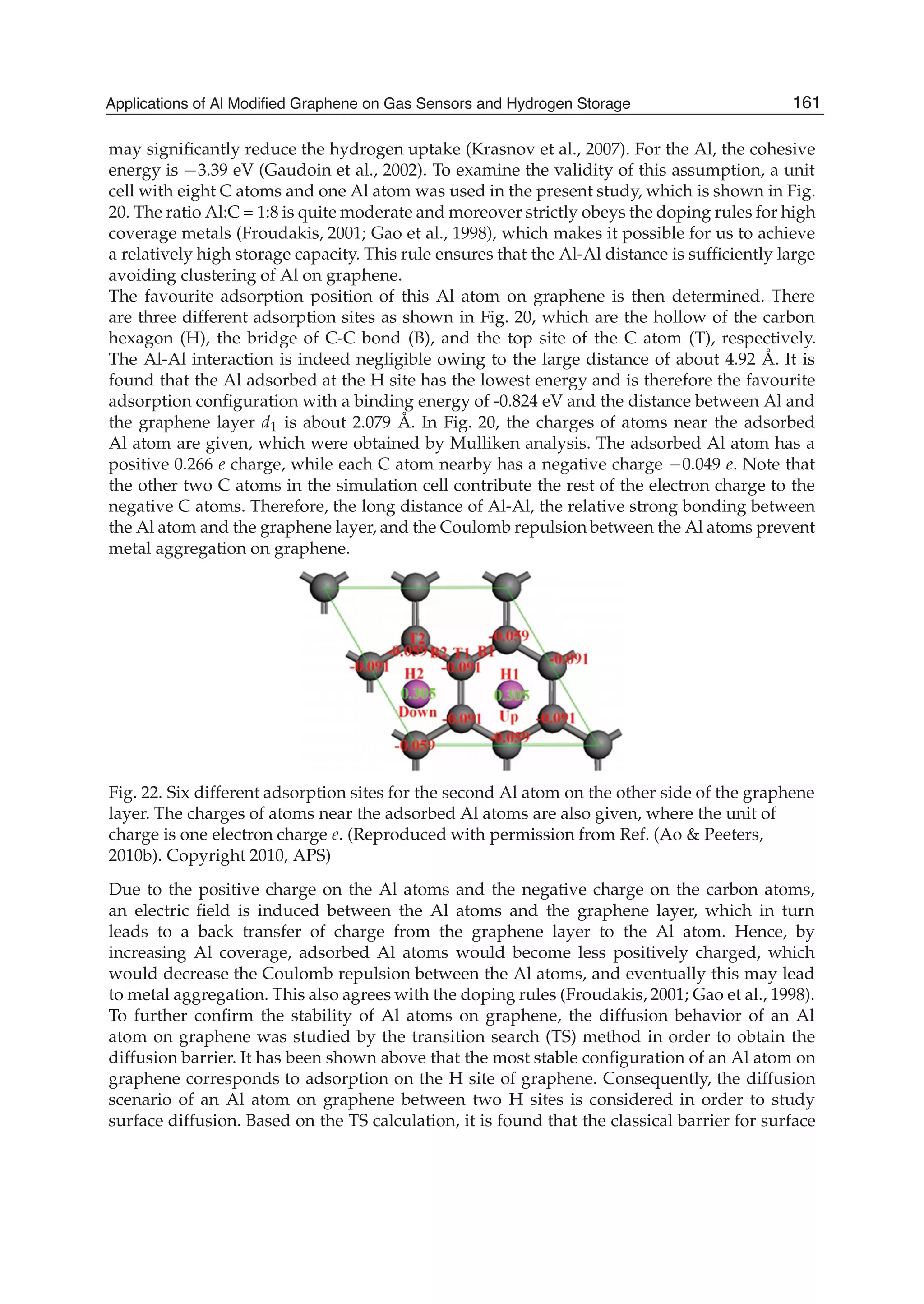
Fig. 20. Three different sites for an Al atom adsorbed on graphene. H, B and T denote the
hollow of hexagon, bridge of C-C bond and top site of C atom, respectively. In addition, the
charges of atoms near the adsorbed Al atom are also given, where the unit of charge is one
electron charge e which is not given in the figure for clarity. The gray and pink balls in this
figure and figures below are C and Al atoms, respectively. (Reproduced with permission
from Ref. (Ao & Peeters, 2010b). Copyright 2010, APS)
LDA was used for all the calculations in this section. All DFT calculations were performed
using the Dmol3 code (Delley, 1990). Double Numerical Plus polarization (DNP) was taken
as the basis set. In this case, three-dimensional periodic boundary conditions were applied
and the H-H bond length was set to lH H = 0.74 Å identical to the experimental value (Lide,
2000). The computational unit cell consists of a 2 2 graphene supercell with a vacuum width
of 18 Å to minimize the interlayer interaction. As shown in Fig. 20, the supercell contains 8 C
atoms. All atoms were allowed to relax in all calculations.
159Applications of Al Modified Graphene on Gas Sensors and Hydrogen Storage](https://image.slidesharecdn.com/grrphysicsandapplicationsofgraphene-theory-140422181144-phpapp02/75/physics-and_applications_of_graphene_-_theory-169-2048.jpg)
![The binding energy of Al atoms onto graphene Eb Al is defined as,
Eb Al = [EnAl graphene (Egraphene + nEAl)]/n (18)
where EnAl graphene, Egraphene and EAl are the energy of the system with n Al atoms adsorbed
on the graphene layer, the energy of the pristine graphene layer and the energy of one Al atom
in the same slab, respectively. The binding energy of H2 molecules onto Al-adsorbed graphene
layer Eb H2 is defined as,
Eb H2 = [EiH2+Al graphene (EAl graphene + iEH2)]/i (19)
where the subscripts iH2+Al-graphene, Al-graphene, and H2 denote the system with i H2
molecules adsorbed, isolated Al-adsorbed graphene and a H2 molecule, respectively.
Fig. 21. A cluster model for 2 H2 molecules adsorbed on graphene with an Al atom adsorbed
on its one side. The white balls are hydrogen atoms in this figure and figures below.
(Reproduced with permission from Ref. (Ao & Peeters, 2010b). Copyright 2010, APS)
To investigate the potential effects of different methodologies on our results, a calculation
using the cluster model was carried out with both LDA and wave function approaches with
the Møller-Plesset second order perturbation (MP2) within the Gaussian modules where the
6 331 + +G basis set was taken and maximum step size was set to 0.15 Å. Note that the
cluster configuration shown in Fig. 21 was used because of the requirement of Gaussian
modules, and the system was recalculated by LDA for purposes of comparison. In this
calculation, a cluster with 24 carbon atoms and with 1 Al atom and 2 H2 molecules adsorbed
over the carbon surface was simulated where the dangling bonds of the C atoms at the
boundary are terminated with H atoms.
On the basis of the published results, one may assume that the uptake capacity of hydrogen
would increase if more metal atoms were adsorbed on the surface of a graphene nanostructure
(Ataca et al., 2009; Liu et al., 2009). Furthermore, the binding between metal atoms and a
surface would be strengthened if more charge is transferred between the metal atoms and
the graphene nanostructure. Obviously, the binding can also be enhanced by adding more
metal atoms with concomitant additional charges available for electronic transfer. However,
metal atoms intend to aggregate into clusters when their concentration is large due to their
high cohesive energies compared with those of metal atoms adsorbed on graphene, which
160 Physics and Applications of Graphene - Theory](https://image.slidesharecdn.com/grrphysicsandapplicationsofgraphene-theory-140422181144-phpapp02/75/physics-and_applications_of_graphene_-_theory-170-2048.jpg)
![Physics and Applications of Graphene - Theory176
are incident upon [Landau & Lifshitz, 1968]. However in relativistic quantum mechanics, a
third scenario can theoretically arise, namely, spatially-bound particles due to the
interaction between particle and antiparticle. Such interplay is unknown in semi-classical or
non-relativistic quantum mechanics, and is rarely observed even in relativistic quantum
mechanics since the requisite electric fields far exceed available technologies. In this article
we will show in Section 3 that this effect can be reproduced in bilayer graphene in the
presence of an antisymmetric potential kink.
1.2 Pseusospin orbital coupling
It is well known that electron spin is coupled to its momentum due to the spin orbit
coupling effect which can be understood via classical electrodynamics or relativistic
quantum mechanics. Dirac’s equation predicts that in the presence of electromagnetic
fields, a single spin particle experiences the Zeeman and the spin orbit coupling effects. In
the latter, one can visualize that an electron traveling with a non-vanishing speed in the
electric field, will in its rest frame “see” an effective magnetic field. The magnetic field
strength depends on the angle between the momentum and the electric field in the plane
which contains both and the field direction is perpendicular to this plane. It is only natural
to envisage that the electron spin will precess about this effective magnetic field and that the
spin precession would be tightly coupled to electron scattering, due to the dependence of
the field strength on the electron motion. What follows is the realization that this
phenomenon has useful device properties; indeed, in the last twenty years, numerous
transistor designs based upon the Rashba and Dresselhaus spin orbit coupling in
semiconductors (Supriyo Datta & B. Das, 1988) have emerged. Bilayer graphene has a
Hamiltonian that resembles the massive Dirac system. This led to the idea that an analogy
of the above might lead to the design of devices similar to spintronics but in the context of
graphene. However, in graphene our focus lies in the pseudospin rather than the real
electron spin. A scientific imperative here is to theoretically ascertain the possible existence
of such pseudospin orbit coupling and details of this would be presented in Section 4 of this
article.
2. Brief introduction to bilayer dynamics
Much has been said about the novelty of graphene which promises new electronics with
applications wild and aplenty. The reduced Hamiltonian of bilayer graphene has been the
center stage for trapping the “bowling ball” and generating a slew of topological dynamics, as
described in Section 1. We will begin with a brief introduction to the full bilayer graphene
Hamiltonian leading to its reduced form. As is well known, the bilayer graphene comprises
two monolayer graphene stacked vertically and has a more complicated energy structure. The
bilayer graphene Hamiltonian (McCann & Fal’ko, 2006) has been expressed as:
1
2
1 1
2
1
2 03
03
0 /2
0 2
A
B
A
B
u / v π cπ
v π u / 2 cπ
H ψ
cπ u t
cπ t u /
ϕ
ϕ
ϕ
ϕ
+⎛ ⎞ ⎛ ⎞⎜ ⎟ ⎜ ⎟⎜ ⎟+ ⎜ ⎟−⎜ ⎟= ⎜ ⎟⎜ ⎟ ⎜ ⎟+⎜ ⎟− ⎜ ⎟⎜ ⎟ ⎝ ⎠⎝ ⎠
(1)](https://image.slidesharecdn.com/grrphysicsandapplicationsofgraphene-theory-140422181144-phpapp02/75/physics-and_applications_of_graphene_-_theory-186-2048.jpg)
![Physics and Applications of Graphene - Theory182
relation for U into Eq. (15) we obtain a hypergeometric equation for V(x) alone with the
solution (Abramowitz & Stegun, 1964)
)(12 zc,b,a,FV(x) = , (16)
ξpc
e
e
(ξ)pb
e
e
ξ)(pa yyy +−=
+
−
−−−=
+
−
+−−= 1),
1
1
1(),
1
1
1( 2
1
2
1 , and z)c,b,(a,F12 is the
Gauss hypergeometric series and the parameters a, b, c depend only on the energy and yp .
(Useful properties of the hypergeometric equation are listed in the Appendix.) The second
equation can be solved similarly:
z)C,B,(A,F
e
ξ)(p
V(x)
2
y
12
1−
+
= , (17)
ξpC
e
e
ξ)(pB
e
e
ξ)(pA yyy ++=
−
+
−−+=
−
+
+−+= 1),
1
1
1(),
1
1
1( 2
1
2
1 , with corresponding
eigenvalue relation 01 =−−+ V)(eUξ)y(p
2
. (A technical point is in order: when solving
the second equation one finds the roles of U and V reversed. This is a veiled signal that
locality is crucial because any assumed nonlocal relation, except possibly for overall sign,
invoked for the first equation would not generally be consistent for the second.) Together
the two relations yield a consistency condition implying an independent equation
relating ξ , e and yp : writing βiαξ += , we solve this equation to obtain α(β) =
1/221/224
])()1[(
2
1
yy pep −+−+ . This ensures the consistency of the ansatz (14) and the
eigenvalue relations: any dependence on x, U, or V has now been eliminated in favor of an
algebraic one involving e and yp alone. Implicit in the above development is the locality of
all the intervening relations, that is, all dynamical relations between u and v occur at the
same spatial point x. The complex conjugates of (16) and (17) are easily seen to be solutions
of Eq. (15) also so we can form a linear combination of these to arrive at the complete
( 0≥x ) solution. Next the above procedure can be repeated for x < 0. Replacing ξ with - ξ
in the ansatz (14) and employing a new auxiliary variable,
x
ey
2
−= , we discover that the
solutions are exactly the same ones (15) and (17) above but with the order reversed and z
replaced by y. The numbers α and β are given by the same relation above. (Thus there are
four solutions of which, for 0≥x ( 0≤x ), we choose α positive (negative). There is no such
restriction on β ). We summarize these results: corresponding to Eq. (16)
0),(12 <= x,c',b',a'FV(x) y (16a)
ξpc'
e
e
(ξpb'
e
e
(ξpa' yyy ++=
−
+
−+=
−
+
++= 1),
1
1
1)(),
1
1
1)( 2
1
2
1 , and to Eq. (17),](https://image.slidesharecdn.com/grrphysicsandapplicationsofgraphene-theory-140422181144-phpapp02/75/physics-and_applications_of_graphene_-_theory-192-2048.jpg)
![Physics and Applications of Graphene - Theory190
where j
j
A/c 0−∂=E is the electric field. We provide the above to merely illustrate the close
connection between the bilayer graphene and the vacuum Dirac Hamiltonian, such that
useful analogies of pseudo-spin orbit coupling to the vacuum spin orbit coupling can be
drawn. Thus, to simplify matter, we temporarily disregard the fact that
3
3
0
0
v
a v
π
π +
⎛ ⎞
⎜ ⎟Δ =
⎜ ⎟
⎝ ⎠
and
0
0
t
b t
⎛ ⎞
Δ = ⎜ ⎟
⎝ ⎠
. Rather we replace
2
32
2
3
( ) 0
0 ( )
a
v p
v p
⎛ ⎞
⎜ ⎟Δ = ⎜ ⎟
⎜ ⎟
⎝ ⎠
with
⎟
⎟
⎠
⎞
⎜
⎜
⎝
⎛
=Δ
2
2
2
0
0
mc
mc
a
so that one can write 2
aΔ ΔI= where 2
Δ mc= . We make an even more
drastic assumption that one can write
2
2
0
0
b
mc
ΔI
mc
⎛ ⎞
⎜ ⎟Δ = =
⎜ ⎟
⎝ ⎠
. With this, Eq.(26) can be
reduced to
χ
Δ-eE
c
θ
b ][V−
⋅
=
pσ
(29)
where ΔΔΔ ab == ][][ 2
. The relativistic energy equation which could be used to describe
the analogous effect of pseudo spin orbit coupling, i.e. the coupling of pseudo spin to
particle momentum in the presence of electric fields, for Dirac fermions in graphene-like
material systems is thus
0)(
][][
)(
b
2
b
2
2222
=
⎥
⎥
⎦
⎤
⎢
⎢
⎣
⎡
×⋅
−−
−⋅
−−
−−− χ
ΔeE
ce
ΔeE
cie
cpΔe-E a pσp EE
VV
V (30)
To avoid excessive details into the material science and band structure of graphene, we will
take the liberty of assuming that the relation II ΔΔΔΔ ba == ;22
is satisfied in bilayer
graphene or, at least, can be realized by material engineering.
We will now investigate the effects of pseudo SO coupling on the pseudo spin χ . As is well-
known, a particle in a SO coupling system experiences an effective magnetic field
E×= pBΕ which couples directly to its momentum vector, thus preserving time-reversal
symmetry. In the technology-relevant field of spintronics, such ΕB can be used to control
the precession of spin when coupled with appropriate momentum constraints (e.g. single
mode one-dimensional ballistic transport), similar to gate bias-controlled spin precession via
Rashba or Dresselhaus SO coupling in the so-called Datta-Das spin transistor (Supriyo,
Datta et al, 1989). On the other hand, spin relaxation is related to electron precession about
ΕB (D’yakonov, M.I. et al, 1971), which suggests that pseudospin relaxation can be analyzed
in analogy to spin relaxation under spin orbit coupling, but in the relativistic limit. In
typical graphene-like materials, ][][ 2
ba ΔΔΔ == is small (10-300 meV for massive
fermion, 0 meV for massless fermion). Since kinetic energy KE << Δ (5 order of magnitude
smaller) for the non-relativistic approximation to apply, the corresponding number of non-](https://image.slidesharecdn.com/grrphysicsandapplicationsofgraphene-theory-140422181144-phpapp02/75/physics-and_applications_of_graphene_-_theory-200-2048.jpg)
![Graphene-Based Devices Based on Topological Zero Modes and Pseudospin Degree of Freedom 191
relativistic particles is very small. For particles confined to energy range 1-2 order of
magnitude smaller than Δ, we consider these particles as relativistic; this prompts the need
to analyze the pseudo SO effect in the relativistic limit. One could visualize the pseudo spin
precessing about an effective magnetic field which could only be “seen” by the pseudo spin,
at a precessional frequency which could be deduced from ])/(2
bΔEep [−= cEω . With
the average velocity given by
][ 2
a
22
2
Δcp
pc
μ χvχ
+
= , the precession angle over the Bloch
sphere of the pseudospin, for a unit of particle travel length in the relativistic regime is given
by:
2
)pcΔ(E
Δc(pe
χvχ
ω
l
Ω
b
a
22
μ ][
])[ 2
−
+
==
E
(31)
A series of pseudospin relaxation has been predicted and analyzed for different energy
regimes. In summary, it has been studied that Dirac particles in the energy range
of 1≈pc meV (which although is relatively small compared to the energy gap of ≈Δ 200 –
300 meV, it is large enough to be within the relativistic regime), Eq. (31) reduces
to 3
cp
Ee
l
Ω Δ
= . Increasing particle’s momentum reduces the precessional angle for a fixed
travel length. By contrast, in the ultra-relativistic limit (i.e. massless Dirac particle), Eq.(31)
reduces to c/eE=Ω l/ , which predicts that massless Dirac particle has a constant l/Ω .
This can be understood as typically, massless particle travels at the effective speed of light in
the medium. In this limit, pseudo spin relaxation becomes independent of particle
momentum. In the non-relativistic limit, where
εχχ =
⎟
⎟
⎠
⎞
⎜
⎜
⎝
⎛
×⋅++ )(
Δ
ec
Ve
2m
p
pσ E2
22
4
, it is found that pχHχ nr
SC E2
2
4Δ
= ce . The average
particle velocity can be approximated as p/mχvχ μ = , and in a similar manner, the
precession angle Ω per unit travelling distance is given by Δ=Ω 4/eEl/ , which is
independent of particle momentum. Therefore in both non-relativistic and ultra-relativistic
limits, l/Ω is independent of the particle momentum. But in the former, l/Ω depends
inversely on Δ ; such a dependence obviously cannot exist in the ultra-relativistic limit
where the coupling mass term vanishes.
Based on the above understanding, we briefly propose that a nanoscale device which
consists of a graphene ring and a charged nano-sized dot at the centre would be a suitable
platform to utilize the pseudospin orbit coupling of the graphene Dirac particles. The
pseudospin orbit strength can be calculated in the relativistic and low energy limits in
analogy to spin orbit coupling in semiconductors. Pseudospin orbit coupling strength can
be enhanced by accelerating the Dirac particles around the ring, due to the small energy gap
in graphene and the large radial electric field due to the charged quantum dot.](https://image.slidesharecdn.com/grrphysicsandapplicationsofgraphene-theory-140422181144-phpapp02/75/physics-and_applications_of_graphene_-_theory-201-2048.jpg)
![Physics and Applications of Graphene - Theory192
5. Conclusions
The zero modes (21) may find possible application in two ways: (a) one can take advantage
of the relation (18) applied to the zero modes as a switching indicator and (b) in so far as
zero modes are of two types associated with the chiral functions T
)1,1( and T
)1,1(− , they
might store information much as binary bits do. The topological properties of the charge
and spin of these zero modes confer a certain degree of robustness to these binary states.
Even the presence of some disorder would not alter this conclusion provided the kink
retains its topological character. An indication of this is that the zero modes appear even for
small r value. Further application of the zero modes can be derived from utilizing the valley
degree of freedom (or “valleytronics” (Rycerz et al., 2007), which can be modified along the
kink direction. Our results would also be of interest in brane theory (Horava, 2005) and
superconductivity (Lu & Yip, 2008). We also describe another relativistic effect in graphene,
namely, pseudospin orbit coupling (pseudo-SOC) effect. Potentially the pseudo-SOC effect
can be used for pseudospin field effect transistor (FET) in much the same way that the
physical spin orbit coupling is used for semiconductor spin-FET. The pseudospin orbit
coupling strength has to be further enhanced for it to be comparable to the conventional
semiconductor-based Rashba effect. Future work which focuses on modifying the graphene
structure can potentially enhance this useful pseudo-SOC effect within experimentally
accessible parameters.
The support of NRF/NUS under Grants Nos. R-143-000-357-281 and R-263-000-482-112 are
gratefully acknowledged.
Appendix
The hypergeometric differential equation is (in general z is complex)
0]1[(1 2
2
=−++−+− wab
dz
dw
)zb(ac
dz
wd
z)z ,
whose solution is the Gauss series
n!
z
z)c;a,(b,Fz)c;b,(a,F
n
n n)Γ(c
n)n)Γ)ΓΓ(a
Γ(a)Γ(b)
Γ(c)
∑==
∞
= +
++
0
1212
with circle of convergence on the unit circle 1=z . The series is not defined when c = 0 or a
negative integer. We also have applied the useful differential relation
)1111212 z,c,b,(aFz)c,b,(a,F
c
ab
dz
d
+++=
When c – a – b is an integer (as in overbarrier scattering), extra care is required to solve the
hypergeometric equation. In this case the following is true: two linearly independent
solutions of
0(1(1(1
2
1
=−−+− − wqp)z)z)z
dz
dw
dz
wd
2
2
,](https://image.slidesharecdn.com/grrphysicsandapplicationsofgraphene-theory-140422181144-phpapp02/75/physics-and_applications_of_graphene_-_theory-202-2048.jpg)
![Physics and Applications of Graphene - Theory196
sheet during the peeling process. The two-component epoxy resin adhesive satisfies the
above condition. If the thickness of the peeled graphene plate is reduced, the comparison
between the present simulation and the experiment will become possible.
Therefore, in this chapter, ahead of experiment, we have theoretically reported the
nanoscale peeling behaviors of the monolayer graphene sheet based on the molecular
mechanics simulation (Sasaki et al., 2009a, 2010). The peeling force curve exhibits the
nanoscale change of the graphene shape from the surface to the line contact. The center
position and the left edge are chosen as the lifting position. In Section 3, the peeling of the
monolayer graphene sheet with the armchair edge for lifting the center position is discussed.
In Secs. 4 and 5, the peeling of the monolayer graphene sheet with the armchair- and zigzag-
edge for lifting the edge position is discussed, respectively.
2. Model and method of simulation
In the simulation, a rectangular-shaped monolayer graphene sheet with each side of 38 Å ×
20 – 21 Å, comprised of 310 carbon atoms, is peeled from the rigid rectangular graphene
sheet (which is called, the ’graphite surface,’ hereafter) with each side of 164-165 Å × 58 Å,
comprised of 3536 carbon atoms [Fig. 1(a)]. First, both the above graphene sheets are
separately optimized by minimizing the covalent bonding energy described by the Tersoff
potential energy (Tersoff, 1988), Vcov, using the Polak-Rebiere-type conjugate gradient (CG)
method (Press et al., 1999). Here the convergence criterion is set so that the maximum of
absolute value of all the forces acting on the movable atoms, becomes lower than 10-5 eV/Å.
Next, the graphene sheet is put and adsorbed onto the graphite surface, so that the AB
stacking registry between the graphene sheet and the graphite surface is satisfied as shown
in Figs. 1(b) and 1(c). Here the green-colored six-membered ring at the center position or the
outermost left edge of the graphene sheet is assumed to be attached to the AFM tip apex
[Fig. 1(a)], and then it is gradually moved upward along the z direction, parallel to the
[0001] axis, by 0.1 Å. For each lifting position of the graphene sheet, z, the total energy Vtotal
=Vcov + VvdW, is minimized using the CG method, where VvdW is the nonbonding vdW
interaction described by the modified Lennard-Jones (LJ) potential energy (Lu et al., 1988,
Stoddard and Ford, 1973), acting between the graphene sheet and the graphite surface. Thus
the optimized positions of the movable carbon atoms of the graphene sheet, (x, y, z), the
vertical peeling force Fz, and the lateral sliding forces Fx and Fy, acting on the lifting center,
are calculated during the peeling process. In this paper, the graphene sheets with armchair-
[Fig. 1(b)] and zigzag-edges [Fig. 1(c)] are discussed.
3. Center-lifting case of armchair-edge graphene
When the six-membered ring located at the center position of the monolayer graphene sheet
is lifted, the graphene sheet exhibits the characteristic transition of its shape during the
peeling process within the x-z plane as illustrated in Figs. 2A-2J, corresponding to Figs. 3A-
3J, the vertical force acting on the lifting center position Fz plotted as a function of the
displacement from the initial position along z-direction, z. At first the monolayer graphene
sheet takes an initial planar structure parallel to the rigid graphite surface [Fig. 2A: z = 0 Å].
Here the surface contact is formed between the graphene sheet and the graphite surface. The
vertical force Fz is zero [Fig. 3A]. Just after the beginning of the peeling [Fig. 2B: z = 2.0 Å],
the attractive interaction force takes the minimum value, –3.1eV/Å [Fig. 3B].](https://image.slidesharecdn.com/grrphysicsandapplicationsofgraphene-theory-140422181144-phpapp02/75/physics-and_applications_of_graphene_-_theory-206-2048.jpg)
![Simulated Nanoscale Peeling Process of Monolayer Graphene Sheet-
Effect of Edge Structure and Lifting Position 197
164 Å
x
y
z x
y
x
y
z x
y
58 Å 21 Å
38 Å
Rigid rectangular
graphite surface:
3536 atoms
Armchair edge
x
y
z x
y
x
y
z x
y
165 Å
58 Å
38 Å
20 Å
Rectangular monolayer
graphene sheet: 310 atoms
Rigid rectangular
graphite surface:
3536 atoms
Zigzag edge
Rectangular monolayer
graphene sheet: 310 atoms
(b)
(c)
free edge
(outermost array)
lifting edge
2nd arraylifting edge
free edge
(outermost array)2nd array
lifting center
164 -165 Å
58 Å
38 Å
20-21Å[0001]
z y
x
z y
x Graphite surface
Graphene sheet
Peeling
lifting
center
AFM tip apex
(a)
z z
lifting
edge
Fig. 1. (a) The schematic illustration of the model of the monolayer graphene sheet
physically adsorbed onto the rigid graphite surface used in the simulation. The green-
colored six-membered ring at the center position or left edge of the graphene sheet is
assumed to be adsorbed onto the atomic force miroscopy tip apex indicated by broken lines,
and it is moved upward along the z (or [0001]) direction, by z = 0.1 Å. Initial AB stacking
registry of the red-colored graphene sheet with (b) armchair and (c) zigzag edge adsorbed
onto the blue-colored graphite surface within the x - y plane.](https://image.slidesharecdn.com/grrphysicsandapplicationsofgraphene-theory-140422181144-phpapp02/75/physics-and_applications_of_graphene_-_theory-207-2048.jpg)
![Physics and Applications of Graphene - Theory198
A 0.0 B 2.0 C 2.1 D 2.4 E 2.5
x
z
surface contact surface contact
F 5.0 G 7.3
surface contact line contact
H 10.0
line contact line contact
I
14.8
peeling
J 14.9
Fig. 2. The transition of the shape of the monolayer graphene sheet during the peeling
process from A to J within the x - z plane. The red-colored graphene sheet and blue-colored
graphite surface are shown. The displacement of the lifting center position from the initial
position, z [Å], is indicated on the upper-right positions of each picture.
Fig. 3. The vertical force, Fz, acting on the center six-membered ring, plotted as a function of
the lifting displacement z. The positions A-J correspond to those of Fig.2.
Between z = 2.0 Å and 2.1 Å, the first discrete partial peeling of the graphene occurs [Figs.
2B →2C], which produces the 1st discontinuous jump in the force curve [Figs. 3B →3C].
The partial peeled area around the lifting center of the graphene is shown in Figs. 4B →4C.
Then, between z = 2.4 Å and 2.5 Å, the second discrete partial peeling of the graphene occurs
[Figs. 2D →2E], which produces the 2nd discontinuous jump in the force curve [Figs.
3D →3E]. The partial peeled area of the graphene is shown in Figs. 4D →4E. Which of
these two areas is peeled first is expected to be actually the stochastic process under the](https://image.slidesharecdn.com/grrphysicsandapplicationsofgraphene-theory-140422181144-phpapp02/75/physics-and_applications_of_graphene_-_theory-208-2048.jpg)
![Simulated Nanoscale Peeling Process of Monolayer Graphene Sheet-
Effect of Edge Structure and Lifting Position 199
room temperature condition. Now the surface contact region is split into the left and right
sections [Fig. 2E]. After the two discrete jumps, Fz increases as the peeling proceeds, since
the attractive surface contact region gradually decreases [Fig. 2F: z = 5.0 Å]. Then the surface
contact continuously turns into the line contact at z = 7.3 Å [Fig. 2G]. Here the ’line contact’
is defined by the following two criteria: 1) The carbon atoms on the left and right outermost
arrays of the graphene sheet [Fig. 1(b)] receive the repulsive interaction force from the
graphite surface. 2) The carbon atoms on the second arrays [Fig. 1(b)] next to the outermost
arrays receive the attractive interaction force. As illustrated in Fig. 5, the average forces
acting on one carbon atom on the outermost and the second arrays satisfy the above criteria
at z = 7.3 Å, which corresponds to Fig. 2G.
B
2.0
C
2.1
D
2.4
E
2.5
I
14.8
J
14.9
Peeled area
Peeled area
Fig. 4. The atomic structures of the graphene sheet just before and after the discrete change,
B →C, D →E, and I →J. The regions surrounded by dotted ellipses show the partial
peeled areas.
Fig. 5. The averaged forces acting on one atom on the left and right outermost arrays (red-
colored) and those on the left and right second arrays (blue-colored), as a function of the
displacement of the lifting center position from the initial position, z [Å].](https://image.slidesharecdn.com/grrphysicsandapplicationsofgraphene-theory-140422181144-phpapp02/75/physics-and_applications_of_graphene_-_theory-209-2048.jpg)
![Physics and Applications of Graphene - Theory200
Once the line contacts are formed between the free edges (outermost arrays) of the peeled
graphene sheet and the graphite surface, they clearly slide on the graphite surface as
indicated by a circle in Figs. 2G →2H →2I with a rapid increase of the bending of the
graphene sheet. Within x-y plane, the right outermost array of the graphene sheet slides
nearly straightforward along -x direction, not so sensitive to the lattice structure of the
surface as illustrated in Figs. 6(a) and 6(b), which show the trajectories of the two carbon
atoms on the right outermost array illustrated in Fig. 1(b). The sliding of the outermost
arrays during G and I appears much more clearly than that during A and G, During H and I,
the decrease of Fz [Figs. 3H and 3I] can be explained by the decrease of the repulsive force
acting on the carbon atoms on the left and right edges of the graphene sheet as shown in
Fig. 5, that’s to say, the relative increase of the effect of the attractive interaction force.
10 15 20
0
2
(a)
x [Å]
y [Å]
I H G F A
19.9 20 20.1 20.2
0
1
2
(b)
ABCD
E
x [Å]
y [Å]
Fig. 6. The trajectory of the two carbon atoms on the right free edge (outermost array)
indicated by white circles in Fig. 1(b). (a) The whole trajectory A →I, and (b) the part of the
trajectory A →E, including the discrete jumps, B →C and D →E, are indicated. White
circles mean carbon atoms of the graphite surface. The indices A – I correspond to those in
Fig. 2.
Fig. 7. The lateral force, Fy, acting on the center six-membered ring, plotted as a function of
the displacement z. The positions A-J correspond to those of Fig. 2.](https://image.slidesharecdn.com/grrphysicsandapplicationsofgraphene-theory-140422181144-phpapp02/75/physics-and_applications_of_graphene_-_theory-210-2048.jpg)
![Simulated Nanoscale Peeling Process of Monolayer Graphene Sheet-
Effect of Edge Structure and Lifting Position 201
When the bending of the graphene sheet becomes larger than a certain range, both the left
and right line contacts break and the graphene sheet is completely peeled from the surface
[Figs. 2I →2J: z = 14.8 Å →14.9 Å], which produces the 3rd discontinuous jump in the force
curve [Figs. 3I →3J]. As illustrated in Figs. 2I →2J, and Figs. 4I →4J, the graphene sheet
exhibits the transition from the arched shape to the planer shape.
Thus the vertical peeling force Fz exhibits the characteristic shape as shown in Fig. 3, which
reflects the transition from the surface to the line contact between the graphene sheet and
the graphite surface. On the other hand, the lateral sliding force Fx is zero due to the
structural symmetry of the system. However, the lateral sliding force Fy shows a finite value
with an oscillation whose period and amplitude decreases as z increases. This oscillation of
Fig. 7 reflects the trajectory of the graphene edges illustrated in Fig. 6 at the graphene -
substrate interface during the peeling process. The maximum lateral force Fy ≈ 0.1 eV/Å
which is only about 3 % of the absolute value of the maximum adhesion force |Fz|= 3.1
eV/Å.
4. Edge-lifting case of armchair-edge graphene
4.1 Nano-scale peeling along vertical direction
When the left edge of the monolayer graphene sheet with armchair edge [Fig. 1(b)] is lifted,
the shape of the graphene sheet markedly changes during the peeling process within the x-z
plane as illustrated in Figs. 8A-8J, corresponding to Figs. 9(a)A-9(a)J, the vertical force acting
on the lifting edge Fz plotted as a function of the edge height z.
A 0.0 6.1C D1.1B E 31.2
GF 31.3 33.9 J 38.4
surface contact surface contactsurface contact surface contact surface contact
line contact line contact
x
z
x
z
18.3
line contact
37.9 38.0H I
Fig. 8. The transition of the shape of the monolayer graphene sheet with free edge of
armchair-type during the peeling process from A to J within the x - z plane. The red-colored
graphene sheet and blue-colored graphite surface are shown. The height of the lifting left
edge z [Å] are indicated on the upper-right positions of each picture.
Surface-contact region At first the monolayer graphene sheet takes an initial planar structure
parallel to the rigid graphite surface [Fig. 8A: z = 0 Å], and the vertical force Fz is zero
[Fig. 9(a)A], which means the graphene sheet completely takes the surface contact with the
graphite surface. Just after the start of the peeling [Fig. 8B: z = 1.1 Å], the attractive interaction
force |Fz| becomes the maximum, 0.74 eV/Å [Fig. 9(a)B]. After that the surface contact area
gradually decreases as the peeling proceeds [Figs. 8C-8E], where Fig. 9(a) exhibits the atomic-
scale zigzag structures [Figs. 9(a)C-E], which will be explained in Section 4.2.](https://image.slidesharecdn.com/grrphysicsandapplicationsofgraphene-theory-140422181144-phpapp02/75/physics-and_applications_of_graphene_-_theory-211-2048.jpg)
![Physics and Applications of Graphene - Theory202
0 20 40
–0.6
–0.4
–0.2
0
Forceactingonthe
liftingedgeFz[eV/Å]
A
B
D
C
E
F
G
I
H
J
(a)
line
contact
surface contact
I: 38.0F: 31.3
I II III IV V VI VII
0 20 40
0
0.05
The outermost
array
The second
array
(b)
E
F
E
F
line
contact
surface contact
I
H
H
I
Forceactingonthe
liftingedgeFz[eV/Å]
Lifting edge height z [Å]
Fig. 9. (a) The vertical force Fz acting on the lifting edge, plotted as a function of the lifting
edge height z for the graphene with armchair-type free edge. The indices A-J correspond to
those of Fig. 8. (b) The red-colored averaged force per one atom acting on the outermost
array, and the blue-colored one acting on the second array, as a function of the lifting edge
height z [Å]. The indices E, F, H and I correspond to those of Figs. 8 and 9(a).
Line-contact region After the surface contact vanishes, the line contact appears [Fig. 8F]. Here
the ’line contact’ is defined by the following two criteria similar to the case of the center-
lifting peeling: 1) The outermost array of the free edge of the graphene sheet [Fig. 1(b)]
receives the averaged repulsive interaction force per one carbon atom from the graphite
surface. 2) The second array next to the outermost array [Fig. 1(b)] receives the averaged
attractive interaction force per one carbon atom. As illustrated in Fig. 9(b), the edge height z
= 31.3 Å satisfies the above criteria [Fig. 8F]. Here the free edge adsorbed onto the graphite
surface is nearly fixed even if the left edge is lifted [Fig. 8F →Fig. 8G: z = 33.9 Å]. As a result
the in-plane bending of the graphene sheet markedly decreases, and|Fz| decreases to zero](https://image.slidesharecdn.com/grrphysicsandapplicationsofgraphene-theory-140422181144-phpapp02/75/physics-and_applications_of_graphene_-_theory-212-2048.jpg)
![Simulated Nanoscale Peeling Process of Monolayer Graphene Sheet-
Effect of Edge Structure and Lifting Position 203
[Figs. 9(a)F-G]. After that the free edge slides on the surface until the graphene sheet takes
planar structure within the y-z plane [Fig. 8H: z = 37.9 Å], where |Fz| increases again
[Fig. 9(a)H].
Toward complete peeling Then the graphene sheet is continuously moved upward [Fig. 8I: z =
38.0 Å → Fig. 8J: z = 38.4 Å], and is completely peeled from the surface. It is noted the line
contact clearly vanishes at z = 38.0 Å [Fig. 9(b)I]. The attractive interaction force |Fz|
increases to take the maximum value [Figs. 9(a)I →J], and then it gradually decreases to
zero toward the complete peeling.
4.2 Atomic-scale sliding within lateral plane
Fig. 9(a) shows the atomic-scale zigzag structures within the surface- and line-contact
regions, which can be explained by the following atomic-scale sliding motions of the
graphene sheet within the x-y plane.
Surface-contact region During the surface contact region between C and E in Fig. 9(a), z-Fz
curve takes the atomic-scale zigzag structures from I to VII. The zigzag behaviors exhibit the
transition from the continuous [Figs. 10(a)I - II] to the sawtooth shapes [Figs. 10(a)III - VII].
First Figs. 10(a)1 →2 →3 →4 →5 correspond to Figs. 10(b) 1 →2 →3 →4 →5, which
show that the graphene sheet continuously slides passing over the nearest neighboring AB
stacking sites with the graphite surface. The trajectories of the graphene sheet exhibit the
continuous zigzag paths as shown in Fig. 10(b)5. Next Figs. 10(a) 6 →7 →8 →9 →10
correspond to Figs. 10(c) 6 →7 →8 →9 →10 which show that the graphene sheet takes
the zigzag stick-slip motions between the nearest neighboring AB stacking sites. Just before
the slip, the graphene sheet deviates quite a little from the AB-stacking site [Fig. 10(c)6: z =
17.3 Å]. Then it discretely jumps or slips to the neighboring AB-stacking site [Fig. 10(c)7: z =
17.4 Å]. As the peeling proceeds, the graphene sheet continuously slides quite a little
[Fig. 10(c)8: z = 18.2 Å], then it discretely slips again to the neighboring AB stacking site
[Fig. 10(c)9: z = 18.3 Å]. After that the graphene sheet continuously slides quite a little again
[Fig. 10(c)10: z = 20.1 Å] until the next slip toward the neighboring AB stacking site occurs.
As a result the trajectories of the graphene sheet exhibit the discrete zigzag paths connecting
the nearest neighboring AB-stacking sites as shown in Fig. 10(c)10. The period of the zigzag
behavior of the Fz curve decreases from 3.7Å to 2.5 Å as shown in Fig. 10(a) as the peeling
proceeds. The lattice spacing of the graphite surface, 2.5 Å, appears in the peeling force
curve particularly for the stick-slip region.
Line-contact region During the line contact region between G and H in Fig. 9(a), z-Fz curve
takes another atomic-scale zigzag structures as shown in Fig. 11(a). One of the zigzag
behaviors in the force curve [Figs. 11(a) 1 →2 →3] corresponds to the stick-slip sliding
motions of the graphene sheet [Figs. 11(b) 1 →2 →3]. Here the free edge of the graphene
sheet slides with nearly the straight stick-slip motions. One of the carbon atoms on the free
edge passes over the carbon-carbon bonds as shown in Figs. 11(b)1 and 3.
5. Edge-lifting case of zigzag-edge graphene
Recently it has been reported that the edge structure of the graphene sheet plays quite an
important role in electronic, magnetic and optical properties of graphene, which can be also
expected to give influences on the mechanical properties such as the peeling process.
Therefore, in this section, the peeling process of the graphene sheet with zigzag edge is](https://image.slidesharecdn.com/grrphysicsandapplicationsofgraphene-theory-140422181144-phpapp02/75/physics-and_applications_of_graphene_-_theory-213-2048.jpg)
![Physics and Applications of Graphene - Theory204
10 20 30
–0.5
–0.4
–0.3
x
y
z x
y
z
1
2
4
3
5
(a)
(b)
Lifting edge height z [Å]
Forceactingonthe
liftingedgeFz[eV/Å]
1: 7.5Å 2: 8.6Å
3: 8.9Å 4: 9.8Å
5: 11.2Å
3.7Å
x
y
z x
y
z
(c) 6: 17.3Å 7: 17.4Å
8: 18.2Å 9: 18.3Å
10: 20.1Å
slip
slip
‘Continuous
sliding’
6
7
8
9=D
‘Stick-slip
sliding’
3.1Å 3.0Å 2.7Å 2.7Å 2.6Å 2.5Å
C 10
stick
continuous stick-slip
I II III IV V VI VII
2.5Å
2.5Å
Fig. 10. (a) Enlargement of part of the z - Fz curve (Fig. 9(a)) corresponding to the continuous
and stick-slip process during the surface contact. (b) The trajectories of the two carbon atoms
on the free edge from 1 to 5 indicated in (a). (c) The trajectories of the two carbon atoms on
the free edge from 6 to 10 indicated in (a).](https://image.slidesharecdn.com/grrphysicsandapplicationsofgraphene-theory-140422181144-phpapp02/75/physics-and_applications_of_graphene_-_theory-214-2048.jpg)
![Simulated Nanoscale Peeling Process of Monolayer Graphene Sheet-
Effect of Edge Structure and Lifting Position 205
36 37 38
–0.1
0
x
y
z x
y
z
1
2
H
3
(a)
(b) 1: 35.9Å 3: 36.7Å2: 36.6Å
stick
stick
slip
slip over the
carbon bond
Lifting edge height z [Å]
Forceactingonthe
liftingedgeFz[eV/Å]
0.6Å 0.5Å0.8Å
0.2Å
slip over the
carbon bond
‘Nearly straight stick-slip sliding’
Fig. 11. (a) Enlargement of part of the z - Fz curve (Fig. 9(a)) corresponding to the nearly
straight stick-slip region during the line contact. (b) The trajectories of the two carbon atoms
on the free edge from 1 to 3 indicated in (a).
discussed. In the simulation, the model obtained by rotating Fig. 1(b) by 30° is used
[Fig. 1(c)], and the left zigzag edge is lifted to simulate the peeling process, while the right
free edge is zigzag type. As a result, the nanoscale peeling process within the x-z plane and
the global shape of the force curve [Fig. 12] is similar to Figs. 8 and 9, respectively. The
qualitative tendency of the decrease of the period and amplitude of the force curve [Fig. 12I-
IV] is similar to that for Fig. 9(a)I-VII. However the details of the atomic-scale mechanics of
the zigzag edge are clearly different from those of the armchair edge as follows:
During the surface contact, the graphene sheet first takes zigzag [Figs. 13(b)1-6] and then
straight stick-slip motions [Figs. 13(c)7-11], passing over the nearest neighboring AB-
stacking site along [1010] direction. It is noted, to avoid AA-stacking registry, the graphene
sheet takes zigzag slip toward the nearest neighboring AB-stacking site as shown in
Fig. 13(b)1 →2, although it then takes straight slip as shown in Fig. 13(c)7 →8. The
minimum period of the force curve of 4.4 Å [Fig. 13(a)IV] reflects the lattice period of the
graphite surface along the [1010] direction, while 2.5 Å for the armchair-type edge
[Fig. 10(a)VII] reflects that along the [1230] direction. Thus the edge structure gives the
marked effects on the atomic-scale dynamics depending on the lattice orientation of the
surface.](https://image.slidesharecdn.com/grrphysicsandapplicationsofgraphene-theory-140422181144-phpapp02/75/physics-and_applications_of_graphene_-_theory-215-2048.jpg)
![Physics and Applications of Graphene - Theory206
Lifting edge height z [Å]
Forceactingonthe
liftingedgeFz[eV/Å]
0 20 40
–0.6
–0.4
–0.2
0
line
contact
surface contact
I II III
IV
38.032.8
Fig. 12. The vertical force Fz acting on the lifting edge, plotted as a function of the lifting
edge height z for the graphene with zigzag-type free edge
During the line contact, the difference between the armchair- and zigzag-type edge is
enhanced. Fig. 14(a) reflects the zigzag stick-slip motion of the graphene sheet [Figs. 14(b)1-
9] unlike nearly the straight stick-slip motion [Figs. 10(b)1-3]. Important point of the line-
contact sliding is that each carbon atom on the free edge takes stick-slip motion between the
nearest neighboring six-membered rings. When each atom is located on the hollow site of
the six-membered ring, the graphene sheet does not deform along the y direction
[Figs. 14(b)1, 4-5, and 8-9]. However, when each atom is located a little far from the hollow
site or near the carbon bond, the graphene sheet bends toward the y direction to decrease
the total interaction energy [Figs. 14(b)2-3 and 6-7]. Thus, in the case of the zigzag-type edge,
collective motion of the single carbon ’atom’ on the free edge nearly dominates the graphene
mechanics together with its deformation. On the other hand, for the armchair-type edge,
collective motion of the single carbon ’bond’ is dominant.
6. Discussions and conclusions
In this chapter molecular mechanics study of the nanoscale peeling of the monolayer
graphene sheet has been performed. The peeling force curve clearly exhibits the change of
the graphene shape from the surface- to the line-contact.
In Section 3, the peeling of the monolayer graphene sheet with the armchair edge for lifting
the center position is discussed. It is noted that the maximum lateral sliding force Fx ≈
0.1 eV/Å is only about 3 % of the absolute value of the maximum adhesion force |Fz|≈
3.1 eV/Å. This small sliding force Fx is derived from the superlubricity at the interface
between the graphene sheet and the graphite surface (Sasaki et al., 2007) and atomic-scale
wear (Sasaki et al., 2009c). There is possibility that such anisotropy between the vertical](https://image.slidesharecdn.com/grrphysicsandapplicationsofgraphene-theory-140422181144-phpapp02/75/physics-and_applications_of_graphene_-_theory-216-2048.jpg)
![Simulated Nanoscale Peeling Process of Monolayer Graphene Sheet-
Effect of Edge Structure and Lifting Position 207
10 20 30
–0.5
–0.4
–0.3
x
y
z x
y
z
1
2
4
3
5
(a)
(b)
Lifting edge height z [Å]
Forceactingonthe
liftingedgeFz[eV/Å]
x
y
z x
y
z
(c)
6
7
8
9
10
1: 11.5Å 2: 11.6Å 3: 12.0Å
4: 12.1Å 5: 14.0Å 6: 14.2Å
7: 17.1Å 8: 17.2Å
9: 19.0Å 10: 19.1Å
11: 22.1Å
slip
stick
slip
stick
‘Zigzag
stick-slip
sliding’
4.4Å
slip
stick slip
‘Straight
stick-slip
sliding’
5.6Å 5.0Å 4.4Å
I II III IV
11
6.9Å
4.4Å
Fig. 13. (a) Enlargement of part of the z - Fz curve (Fig. 12(b)) corresponding to the zigzag
and straight stick-slip process during the surface contact. (b) The trajectories of the two
carbon atoms on the free edge from 1 to 6 indicated in (a). (c) The trajectories of the two
carbon atoms on the free edge from 7 to 11 indicated in (a).](https://image.slidesharecdn.com/grrphysicsandapplicationsofgraphene-theory-140422181144-phpapp02/75/physics-and_applications_of_graphene_-_theory-217-2048.jpg)
![Physics and Applications of Graphene - Theory208
35 36 37 38
–0.25
0
x
y
z x
y
z
(a)
(b)
stick
slip
Lifting edge height z [Å]
Forceactingonthe
liftingedgeFz[eV/Å]
1: 35.6Å 2: 35.7Å 3: 36.1Å
4: 36.2Å 5: 36.9Å 6: 37.0Å
7: 37.2Å 8: 37.3Å 9: 37.8Å
slip stick slip
stickslip
stick slip
‘Zigzag stick-slip sliding’
1
2 3
0.9Å1.3Å
4
5
6
7 8
9
Fig. 14. (a) Enlargement of part of the z - Fz curve (Fig. 12(b)) corresponding to the zigzag
stick-slip process during the line contact. (b) The trajectories of the two carbon atoms on the
free edge from 1 to 9 indicated in (a).](https://image.slidesharecdn.com/grrphysicsandapplicationsofgraphene-theory-140422181144-phpapp02/75/physics-and_applications_of_graphene_-_theory-218-2048.jpg)
![Simulated Nanoscale Peeling Process of Monolayer Graphene Sheet-
Effect of Edge Structure and Lifting Position 209
force Fz and the lateral sliding force Fx can be applied to the adhesives, which can be
strongly adhered to the substrate but can easily slide on it. Our AFM measurement exhibits
that the maximum pull-off force is about several hundreds of nN, which is clearly much
larger than the binding force, 3 eV/Å≈ 4.8 nN, assumed in our simulation.
In Secs. 4 and 5, the peeling of the monolayer graphene sheet with the armchair- and zigzag-
edge for lifting the edge position is discussed, respectively. The atomic-scale sliding motion
of the monolayer graphene sheet during the peeling process is found. For the graphene
sheet with armchair edge, the transition from the continuous to the stick-slip motion of the
graphene sheet is found, which can be explained as follows: The peeling process induces the
increase of the peeled area of the graphene sheet, and the decrease of the surface contact
area. Considering the peeled area of the graphene sheet acts as an effective spring as shown
in Fig. 15, the increase of the peeled area makes the effective spring softer, and the decrease
of the surface contact area decreases the energy barrier to slide the graphene sheet. Finally
the peeling process induces the transition from the continuous to the stick-slip sliding
motion of the graphene sheet, together with the decrease of the period and amplitude of the
z-Fz curve. Important point is that the period of the peeling force curve for the armchair-
edge graphene for the surface contact region corresponds to the lattice spacing of the
graphite surface along [1230] direction, 2.5 Å. On the other hand, for the zigzag-edge
graphene, the period becomes the lattice spacing along [1010] direction, 4.4 Å. This means
the sliding length of the graphene sheet along x direction becomes nearly equal to the peeled
length along z direction. The zigzag structures of the peeling force curve with the same
period of about several Å have been also observed by our preliminary experiments using
the multilayered graphene, which will be reported elsewhere. Of course, if the number of
the peeled graphene sheets is reduced, the direct comparison between the present
simulation and the experiment will become possible.
As a result, the center-lifting case requires the largest attractive peeling force, -3.1 eV/ Å, in
order to peel the graphene sheet as shown in Fig. 16(a). On the other hand, the edge-lifting
case requires only -0.74 eV/Å, about 20 % of that for the center-lifting case as shown in
Figs. 16(b) and 16(c). The edge structures give little influences on the basic features of the
force curve. However, the sliding direction and the edge structure clearly gives marked
influences on the surface- and line-contact regions, respectively.
Another important point is that the behavior of the lateral force curve Fx(z) is qualitatively
the same as that of the vertical force curve Fz(z) during the surface contact as shown in
Fig. 9(b). Therefore it can be said that the peeling force curve, Fz(z), directly reflects the
atomic-scale friction force, Fx(z), which decreases to 0.019 eV/Å≈ 30 pN for z = 27.8 Å
[Fig. 9(b)]. This ultralow friction force Fx is derived from the superlubricity at the interface
between the graphene sheet and the graphite surface (Sasaki et al., 2007, 2009c, Itamura
2009a, 2009b) . Furthermore effect of the edge structure on the peeling process is clarified by
comparison of the free edge between the armchair- and zigzag-types. As mentioned above,
the atomic-scale structure of the force curve during the surface contact reflects the lattice
spacing of the graphite surface. So the minimum period of the atomic-scale structure of the
force curve can tell us the atomic-scale lattice orientation and structure of the free edge of
graphene. Such information can be used for the control of the electronic properties of the
graphene sheet adsorbed onto the substrate. Therefore this paper indicates the possibility of
the identification of the lattice orientation and the edge structure of the graphene sheet.](https://image.slidesharecdn.com/grrphysicsandapplicationsofgraphene-theory-140422181144-phpapp02/75/physics-and_applications_of_graphene_-_theory-219-2048.jpg)
![Physics and Applications of Graphene - Theory210
10 20 30
–0.1
0
0.1
0.3
0.4
0.5
6.1C
D
surface contact
surface contact
18.3
Fz
Fx
Fx
Fz
Fx
Fx
(a)
(b)
Fx
[eV/Å]
-Fz
[eV/Å]
Lifting edge height z [Å]
I II III IV V VI VII
0.019 eV/Å
I II III IV V VI VII
Fig. 15. (a) Schematic illustration of the increase of the peeled area and the decrease of the
surface contact area from C (z = 6.1 Å) to D (z = 18.3 Å) for the graphene sheet with
armchair-type free edge. (b) – Fz and Fx plotted as a function of the edge height z, show
qualitatively the same behavior to each other for the graphene sheet with armchair-type free
edge.
In this chapter, we discussed the importance of the dynamics of the free edge during the
peeling process. On the other hand, we also found the importance of the shape of the graphene
sheet. Additional simulated model and results are shown in Fig. 17. As shown in Fig. 17(a),
rectangular graphene sheet whose aspect ratio is different from that of the graphene](https://image.slidesharecdn.com/grrphysicsandapplicationsofgraphene-theory-140422181144-phpapp02/75/physics-and_applications_of_graphene_-_theory-220-2048.jpg)
![Simulated Nanoscale Peeling Process of Monolayer Graphene Sheet-
Effect of Edge Structure and Lifting Position 211
0 20 40
–3
–2
–1
0
Lifting height z [Å]
VerticalpeelingforceFz[eV/Å]
(a) Center lifting case of
armchair-edge graphene
(b) Edge lifting case of
armchair-edge graphene
(c) Edge lifting case of
zigzag-edge graphene
(a)
(b)
(c)
Fig. 16. Comparison of the vertical forces, Fz, among (a) center-lifting case of the armchair-
edge graphene sheet, (b) edge-lifting case of the armchair-edge graphene sheet, and (c)
edge-lifting case of the zigzag-edge graphene sheet.
sheet of Fig. 1(b) is used. The basic shape of the vertical force curve, Fig. 17(b), is similar to
that of Fig. 3. However the armchair type edge is peeled first for Fig. 17(a), although the
zigzag type edge is peeled first for Fig. 1(b) as discussed in Section 3. This means that the
shape of the graphene sheet plays an important role for deciding which edge is peeled first.
Effect of the graphene shape on the peeling process will be discussed in detail somewhere in
the near future.
Lastly it should be noted that the peeling process discussed in this chapter is closely related
to the atomic-scale wear of the graphite and the graphene tip formation in the friction force
microscopy (Sasaki et al., 2009c). When the tip is pushed onto the surface for less than the
critical tip height, the outermost graphene layer is attached to the FFM tip, which results in
the formation of the graphene tip. In that case, the graphene sheet takes the surface contact
with the second layer graphene, and it takes the two-dimensional stick-slip motion.
However it is difficult to observe directly the stick-slip motion during the scan process, due
to the very small gap between the FFM tip and the graphite surface. On the other hand, if
the peeling process is used, it can be expected that the contact at the AFM tip/graphite
interface has a wider space to be observed directly by ex. Transmission Electron Microscopy
(TEM). This paper indicates the possibility of a direct observation of the stick-slip motion of
the graphene sheet, that’s to say, the elementary process of the atomic-scale friction or
superlubricity which occurs at the tip/graphite surface interface.
This research was supported by a Grant-in-Aid for Scientific Research (B) (No. 20360022)
and for Specially Promoted Research (No. 21000008) from the Japan Society for the
Promotion of Science. This work was also supported by the Ministry of Education, Culture,
Sports, Science and Technology through a Grant-in-Aid for Building Strategic Research
Infrastructures.](https://image.slidesharecdn.com/grrphysicsandapplicationsofgraphene-theory-140422181144-phpapp02/75/physics-and_applications_of_graphene_-_theory-221-2048.jpg)
![Physics and Applications of Graphene - Theory212
Graphite surface
x
y
z x
y
x
y
z x
y
Armchair
edge
lifting center
Zigzag
edge
164 Å
58 Å
21 Å
13 Å
(a)
(b)
0 10 20
–1
0
Displacement z [Å]
ForceactingontheliftingedgeFz[eV/Å]
Fig. 17. (a) The model of the red-colored monolayer graphene sheet physically adsorbed
onto the blue-colored rigid graphite surface within the x – y plane. The green-colored six-
membered ring at the center position is moved upward along the z (or [0001]) direction, by z
= 0.1 Å. Initial AB stacking registry of the red-colored graphene sheet with the blue-colored
graphite surface is assumed. (b) The vertical force Fz acting on the center six-membered ring,
plotted as a function of the lifting displacement z.
7. References
Autumn, K., Liang, Y. A., Hsieh, S. T., Zesch, W., Chan, W. P., Kenny, T. W., Fearing, R., &
Full, R. J. (2000). Adhesive force of a single gecko foot-seta. Nature, Vol. 405, No. 6
(June, 2000) 681-685, ISSN 0028-0836 (print), 1476-4687 (online)
Autumn, K., Sitti, M., Liang, Y. A., Peattie, A. M., Hansen, W. R., Sponberg, S., Kenny, T.
W., Fearing, R., Israelachvili, J. N. & Full, R. J. (2002). Evidence for van der Waals](https://image.slidesharecdn.com/grrphysicsandapplicationsofgraphene-theory-140422181144-phpapp02/75/physics-and_applications_of_graphene_-_theory-222-2048.jpg)
![Simulated Nanoscale Peeling Process of Monolayer Graphene Sheet-
Effect of Edge Structure and Lifting Position 213
adhesion in gecko setae. Proc. Natl. Acad. Sci. U.S.A., Vol. 99, No. 19 (September,
2002) 12252-12256
Geim, A. K. and Novoselov, K. S. (2007). The rise of graphene. Nature Mat., Vol. 6, No. 3
(March, 2007) 183-191, ISSN 1476-1122 (print), 1476-4660 (online)
Ishikawa, M., Kato, M., Harada, R., Sasaki, N. & Miura, K. (2008). Visualization of nanoscale
peeling of carbon nanotube on graphite. Appl. Phys. Lett., Vol. 93, No. 8 (August,
2008) 0831221-0831223, ISSN 0003-6951 (print), 1077-3118 (online)
Ishikawa, M., Harada, R., Sasaki, N. & Miura, K. (2009). Adhesion and peeling forces of
carbon nanotubes on a substrate. Phys. Rev. B., Vol. 80, No. 19 (November, 2009)
1934061-1934064, ISSN 1098-0121 (print), 1550-235x (online)
Itamura, N., Miura, K., & Sasaki, N., (2009a). Analysis of Mechanism of Low Lateral
Stiffness of Superlubric C60 Bearing System. Jpn. J. of Appl. Phys., Vol. 48, (March,
2009) 0302141-0302143, ISSN 0021-4922 (print), 1347-4065 (online)
Itamura, N., Miura, K., & Sasaki, N., (2009b). Simulation of Scan-Directional Dependence of
Superlubricity of C60 Molecular Bearings and Graphite. Jpn. J. of Appl. Phys., Vol.
48, (June, 2009) 0602071-0602073, ISSN 0021-4922 (print), 1347-4065 (online)
Lu, J. P., Li, X. -P. & Martin, R. M. (1988). Ground state and phase transitions in solid C60.
Phys. Rev. Lett., Vol. 68, No. 10 (March, 1992) 1551-1554, ISSN 0031-9007 (print),
1079-7114 (online)
Novoselov, K. S., Geim, A. K., Morozov, S. V., Jiang, D., Zhang, Y., Dubonos, S. V.,
Grigorieva, I. V. & Firsov, A. A. (2004). Electric Field Effect in Atomically Thin
Carbon Films. Science, Vol. 306, No. 5696 (October, 2004) 666-669, ISSN 0036-8075
(print), 1095-9203 (online)
Novoselov, K. S., Geim, A. K., Morozov, S. V., Jiang, D., Katsnelson, M. I., Grigorieva, I. V.,
Dubonos, S. V. & Firsov A. A. (2005). Two-dimensional gas of massless Dirac
fermions in graphene. Nature, Vol. 438, No. 11 (November, 2005) 197-200, ISSN
0028-0836 (print), 1476-4687 (online)
Press, W. H., Teukolsky, S. A., Vetterling, W. T. & Flannery, B. P. (1999). Sec. 10.6
Minimization or Maximization of Functions, In: Numerical Recipes in FORTRAN :
The Art of Scientific Computing, 2nd ed., 413-418, Cambridge Univ. Press, ISBN 0-521-
43064-X, New York
Qu, L., Dai, L., Stone, M., Xia, Z. & Wang, Z. L. (2008). Carbon Nanotube Arrays with Strong
Shear Binding-On and Easy Normal Lifting-Off. Science, Vol. 322, No. 5899
(October, 2008) 238-242, ISSN 0036-8075 (print), 1095-9203 (online)
Sasaki, N., Toyoda, A., Saitoh, H., Itamura, N., Ohyama, M. & Miura, K., (2006). Theoretical
Simulation of Atomic-Scale Peeling of Single-Walled Carbon Nanotube from
Graphite Surface. e-J. Surf. Sci. Nanotech., Vol. 4, (January, 2006) 133-137, ISSN 1348-
0391
Sasaki, N., Itamura, N. & Miura, K. (2007). Simulation of Atomic-Scale Ultralow Friction of
Graphite/C60/Graphite Interface along [1010] Direction. Jpn. J. of Appl. Phys., Vol.
46, No. , (December, 2007) L1237-L1239, ISSN 0021-4922 (print), 1347-4065 (online)
Sasaki, N., Toyoda, A., Itamura, N. & Miura, K., (2008). Simulation of Nanoscale Peeling and
Adhesion of Single-Walled Carbon Nanotube on Graphite Surface. e-J. Surf. Sci.
Nanotech., Vol. 6, (February, 2008) 72-78, ISSN 1348-0391](https://image.slidesharecdn.com/grrphysicsandapplicationsofgraphene-theory-140422181144-phpapp02/75/physics-and_applications_of_graphene_-_theory-223-2048.jpg)
![where E(Q) is the exciton dispersion. The BS equation for the equal-time BS amplitude in the
center-of-mass and reduced coordinates is (Kouzakov & Studenikin, 2005):
ΦQ
(r, R; t, t) = d2
r d2
R dt G(1)
(R + αr, R + αr ; t − t )γ0
×
G(2)
(R − αr , R − αr; t − t)γ0
V(r )ΦQ
(r , R ; t , t ).
(7)
The Fourier transforms of the electron and hole propagators G(τ)(r, r ; t) are define in terms of
the Dirac four component spinors ψκ(r) and the corresponding eigenvalues En = ¯hvF
√
2n/R
(Kouzakov & Studenikin, 2005):
G(τ)
(r, r ; ω) = ∑
κ
ψκ(r)ψ
κ
(r )
¯hω − En ± ı0+ (8)
Here we keep only the positive energy pole contributions, n = 0, 1, 2, ..., and κ = (n, jz, σ),
where jz is the z component of the total angular momentum.
When the translation symmetry is broken by the magnetic field, the Green’s functions can be
written as a product of phase factors and translation invariant parts. The phase factor depends
on the gauge. In the symmetric gauge the Green’s functions are:
G(τ)
(r, r ; ω) = exp ı
e
¯hc
r.A(r ) G(τ)
(r − r ; ω). (9)
The broken translation symmetry requires a phase factor for the BS amplitude:
φQ
(r, R; Ω) = exp ı
e
¯hc
r.A(R) χQ
(r, R; Ω). (10)
The BS equation (7) admits translation invariant solution of the form:
χQ
(r, R; ω) = exp [−ı (Q.R)] χQ
(r; ω). (11)
The Fourier transform of the function χQ(r; ω) satisfies the following BS equation:
χQ
(k; ω) =
d2q
(2π)2
d2p
(2π)2
d2
R
∞
−∞
dΩ
2π
e−ı(q+Q).R
G(1) 1
2
q + k −
e
¯hc
A(R); ¯hω + α(E − Vg) γ0
×
G(2)
−
1
2
q + k −
e
¯hc
A(R); ¯hω − α(E − Vg) γ0
V p − k −
2e
¯hc
A(R) χQ(p; Ω),
(12)
where G(τ) (k; ¯hω) are the Fourier transforms of G(τ) (r; ¯hω).
In the effective-mass approximation the exact fermion Green’s functions G(τ) are replaced by
the corresponding propagator of the free fermions. The translation invariant parts of the free
fermion propagators can be decomposed over the Landau level poles (Gorbar et al., 2002):
219Magnetoexciton Binding Energy in Graphene Bilayers](https://image.slidesharecdn.com/grrphysicsandapplicationsofgraphene-theory-140422181144-phpapp02/75/physics-and_applications_of_graphene_-_theory-229-2048.jpg)

![3. Path integral of coherent states
Let us construct a path integral of the coherent states on a group manifold. Following the
Stone’s approach (17), we discuss the coherent states on a general group G. Let us take D(g),
any g ∈ G, as an irreducible representation of the group. Assume that |0 > is some state in the
space of representation. Then one can define |g > by
|g >= D(g)|0 > . (8)
On the basis of the irreducible representation, Shur’s lemma holds that
1
V(G)
d[g]|g >< g| = 1 (9)
where 1
V(G)
is the volume of the group manifold. In the expression of Eq. (9) d[g] is the Haar
measure on the group.
Let us compute a thermodynamic partition function
Z = Tr(e−βH
) (10)
where β is the imaginary time. In the procedure of calculating the partition function, the
trace is constrained to the representation space on which D(g) acts. Dividing the Matsubara
time-interval β into n parts, and using the Shur’s lemma of Eq. (9), we can write down an
iterated integral
Tr(e−βH) = const. (d[g]d[g ] · · · ) < g|e−βH/n|g >< g |e−βH/n · · · |g > . (11)
where const. is the constant value taken on the representation space. When taking into account
short time intervals, one can express g g + δg, and δg O(δt), so that
< g|e−δtH|g >
≈ 1+ < g|δg > + < g|(−δtH)|g > +O(δt2).
(12)
On taking into consideration up to order O(δt), we can write down the formal path-integral
expression
Tr(e−βH)
= 1
V(G)
d[g]exp( < g|δg > −
β
0 dt < g|H|g >).
(13)
Here d[g] is regarded as the path-integral measure given by the Haar measure at each time
step.
The path-integral expression can be identified as a path integration over a quotient space of
the group. In particular it is noted that a set of the |g > can be different from only a phase so
that the integrand is not sensitive to the phase factor. Now suppose that H is the subgroup
of G, constructed from exponentiating a maximal commuting set of generator, i.e., a maximal
torus. Then |0 > is expressed by an eigenstate of the generators of H which means a state of
definite weight. The |g > are represented by all phase multiples of one another in any one
coset of G/H. And hence the coherent states can be described in terms of a bundle over G/H
with the maximal torus as the gauge group, and the integration is made over the path in G/H.
Let us express the integrand in the coherent-state path integral without any choice of
representatives. In order to make a natural procedure on the independent choice of the
representatives, we define the projection operators as
P(g) = |g >< g|. (14)
227Topological Effects, Index Theorem and Supersymmetry in Graphene](https://image.slidesharecdn.com/grrphysicsandapplicationsofgraphene-theory-140422181144-phpapp02/75/physics-and_applications_of_graphene_-_theory-237-2048.jpg)
![They can be directly projected onto the physically distinct states since they do not have any
phase ambiguity. In the integrand, the first term < g|δg > can be taken to be a gauge
invariant form by using Stokes theorem
Γ=∂Ω
< g|dg >=
Ω
d < g|dg > . (15)
Making use of the identity form
d < g|dg >=< dg|dg >= −Tr(dPPdP), (16)
the first term yields
Γ=∂Ω
< g|dg >= −
Ω
Tr(dPPdP). (17)
The second term in the integrand can be rewritten by
< g|H|g >= Tr(P(g)H). (18)
Hence combination of Eqs. (17) and (18) leads us to the path integral given by (17)
Tr(e−βH
) =
1
V(G/H)
d[g]exp −
Ω
Tr(dPPdP) −
Γ
Tr(P(g)H) . (19)
It is noted that the elements of G/H can only contribute to the integrand, so that the volume
factor of the gauge group H gets out of the path integral.
There are certain subgroups corresponding to the Lie algebra G of a Lie group G. Let us
describe some basic facts about semisimple Lie algebra in brief. Then it is known that the
generators of the G can have a decomposition into a maximally commuting set H = {Hi}, i.e.,
the Cartan subalgebra, and a set of ladder operators, Eα, one for each root vector α ∈ R. The
ladder operators are needed for complexifing the algebra to Gc which results from the group
parameters to get the complex values. The Hi and the Eα hold that
[Hi, Eα] = αiEα. (20)
Assume that |λ > is an eigenvector of the Hi with eigenvalues λi such as
Hi|λ >= λi|λ > . (21)
Then
Eα|λ >= |λ + α > . (22)
The roots may be classified into two sets by an arbitrary hyperplane on a root space. On one
set the root objects are positive roots indicated by α ∈ R+ as increasing the weights while the
others are negative roots, by α ∈ R+ as decreasing the weights. And thus we can take the
greatest weight as a state which is annihilated by all Eα, α ∈ R+.
This decomposition of the Lie algebra is made on some kinds of special subgroup. The Borel
subgroups B± are constructed by exponentiating the algebras B± which are spanned by the
Eα, Hi; α ∈ R±, Hi ∈ Hc. Any g ∈ G can be decomposed into the gaussian factors
g = ζ−hζ+; ζ− ∈ Z−, ζ+ ∈ Z+, h ∈ Hc
+, (23)
228 Physics and Applications of Graphene - Theory](https://image.slidesharecdn.com/grrphysicsandapplicationsofgraphene-theory-140422181144-phpapp02/75/physics-and_applications_of_graphene_-_theory-238-2048.jpg)
![In general we cannot determine difference between the number of zero modes. It is seen that
the above result is independent of t owing to the cancelation of the non-zero eigenvalue term.
Actually we should evaluate Index(K). In order to calculate it practically, we take an
alternative method of heat expansion for calculating Tr(γ5e−tK2
). It says that for general ˆΓ
and ˆD on a two dimensional compact manifold we can expand
Tr(ˆΓe−t ˆD
) =
1
4πt ∑
l≥0
t
l
2 bl(ˆΓ, ˆD), (44)
where Tr indicates the trace of matrices and the integration over coordinates of space. bl denote
expansion coefficients. For ˆΓ = γ5 and ˆD = K2, we have to return to an expression that
is t-independent. For this t-independence, the expansion coefficients should vanish for all l
except for l = 2 under the condition that all the t contributions is canceled out each other.
This allows us to determine the coefficient b2 from the first order term in t in the series of
expansion. For the evaluation, let us take D as D = −ie
μ
ν σν(∇μ − ieAμ). Here e
μ
ν indicates the
zweibein of curved surface metric gμν that defines a local flat frame ηαβ = e
μ
α eν
βgμν while σμ is
the Pauli matrix. Aμ denotes a gauge field. It follows that
K2
= −gμν
∇μ∇ν +
1
4
[γμ
, γν
]Fμν −
1
4
R (45)
where R is curvature, and Fμν = ∂μ Aν − ∂ν Aμ means the field strength. ∇μ indicates a
covariant derivative with respect to gauge and reparametrization transformation.
It is easy to see that the non-zero expansion coefficient b2 is written by
b2 = Tr[γ5(
i
4
[γμ
, γν
]Fμν −
1
4
R)] = 2 B · dS, (46)
where B is the magnetic field given by Bl = 1
2
lμνFμν. The integration has been over the whole
surface. These two independent ways for calculating Tr(γ5e−tK2
) allows u to arrive at the final
formula of the index theorem (8)
Index(K) = ν+ − ν− =
1
2π
B · dS. (47)
It states that the total flux which goes out of the surface is related to the number of zero
modes of the K operator. The curvature doesn’t contribute to the index formula because γ5 is
a traceless operator. Particularly no contribution of curvature is to show an intrinsic property
of two dimensional surfaces. The index theorem leads to an integer number on the compact
surfaces. Therefore B · dS produces the total magnetic monopole charge in discrete values
inside the surface under the Dirac quantization condition of magnetic monopoles.
Using the index theorem, we observe the topological characteristics of graphene. Let us apply
it to graphene and its geometric variants. In a certain configuration of graphene we have to
account for the effective magnetic field on the graphene surface. Some plaquette deformations
give rise to a specific circulation of the vector potential around a loop trajectory. Stokes’s
theorem helps us to have a relation between the circulation of the gauge potential around
a loop γi and the flux of the corresponding magnetic field
γi
A · dr =
Si
B · dS, (48)
232 Physics and Applications of Graphene - Theory](https://image.slidesharecdn.com/grrphysicsandapplicationsofgraphene-theory-140422181144-phpapp02/75/physics-and_applications_of_graphene_-_theory-242-2048.jpg)
![given by including additionally the contributions from the surplus of pentagons or heptagons.
Hence the total flux of the effective gauge field can lead to
Index(H) =
1
2π Si
B · dS =
1
2π ∑
n5−n7
γi
A · dr
=
1
2π
π
2
(n5 − n7) = 3(1 − g) −
3
2
Nend. (51)
The total number of zero modes is equivalent to the sum contributed from each subsector of
a Dirac operator. As a consequence, by adding the two contributions, we arrive at the index
of the Dirac Hamiltonian that describes the graphene molecule. The Index(H) is expressed by
(8)
Index(H) = ν+ − ν− = 6(1 − g) − 3Nend (52)
which is consistent with the exact number of the zero modes if ν+ = 0 or ν− = 0. Therefore
we have obtained the theorem which relates the number of zero modes existed in a certain
graphene molecule to the topological characteristics of its surface.
This result provides the number of zero modes for the familiar cases of graphene molecules.
For example, since a fullerene takes g = 0 and Nend = 0, it is expected that it has six zero
modes which correspond to the two triplets of C60 and of similar large molecules. For the
case of nanotubes, we have g = 0 and Nend = 0. This results in ν+ − ν− = 0 which is in
agreement with previous theoretical and experimental results (20; 21). The index theorem
gives rise to a surprising relation between the topology and the presence of magnetic flux
which is effectively inserted in graphene molecules by geometrical deformations. The number
of these deformations can be associated with the general topological characteristics of the
lattice surface. They are related to the zero modes of a general graphene molecule with the
genus and the number of open faces of its surface.
5.3 G index theorem
To build up supersymmetry over the Dolbeault complex which are associated with
deformation on topology of the lattice (22), we need one of the supercharges, Q2 = ¯∂.
The index theorem leads to a topological invariant under deformations on Q2 and plays an
essential role in formulating the SUSY QM over the twisted Dolbeault complex caused by the
deformation in a graphene system.
Let us describe the general statement of the G-index theorem. Suppose that Q and Q† are
supercharges which have a map from a space of bosonic states to a space of fermionic states
and vice versa. Further let us take a Lie group G generated by Gi. Gi satisfies the commutation
relations with Q and Q† such that (17) where
[Gi, Gj] = i f k
ijGk, [Q, Gi] = 0, [Q†, Gi] = 0, (53)
where f k
ij are structure constants. Gi has also a commutation relation with the Hamiltonian of
Eq. (5)
[Gi, H] = 0. (54)
A supercharacter can be expressed as a supertrace of the group elements
Ξ(eiθi
Gi
) = Tr (−1)F
eiθi
Gi
e−tH
. (55)
234 Physics and Applications of Graphene - Theory](https://image.slidesharecdn.com/grrphysicsandapplicationsofgraphene-theory-140422181144-phpapp02/75/physics-and_applications_of_graphene_-_theory-244-2048.jpg)
![The ordinary trace requires us to take a limit of t → 0. But Eq. (55) does not have any
dependence on t because the non-zero energy levels can not make contributions due to
canceling in pairs between the bosonic and fermionic sectors. But the zero-energy levels can
only give contributions. And these are not dependent on t.
The character is topologically invariant under deformations of the operators Q and Q†. On
deformation let us consider the supersymmetry generator Q of the ordinary N = 1 SUSY QM
on a manifold. In locally geodesic coordinates Q is expressed by
Q = d = ψμ†
∂μ. (56)
When deforming Q, it is changed into the new operator
Qs = d + sιK = ψμ†
∂μ + sKμ
ψμ, (57)
where K denotes a Killing vector field. And then the deformed Hamiltonian is given by
Hs ≡ 2(Qs + Q†
s )2
,
= −∂2
+ s2
|K|2
−
1
2
s[ψ†
μ, ψ†
ν]∂μKν −
1
2
s[ψμ, ψν]∂νKμ. (58)
Now suppose that we decompose the deformed N = 1 SUSY operator into holomorphic and
antiholomorphic sectors because of d = ∂ + ¯∂. Then the G-index theorem can be associated
with a high degree of symmetry on a graphene molecule. Let us take a Lie group G generated
by Gi which satisfies the commutation relations with Q2 and Q†
2 such that
[Gi, Gj] = i f k
ijGk, [Q2, Gi] = 0, [Q†
2, Gi] = 0 (59)
where f k
ij mean structure constants. On graphene, there exists the Hamiltonian H such that
H ≡ −2¯h2
v2
F(Q2 + Q†
2)2
, [Gi, H] = 0. (60)
On deforming Q2, this can be changed into a new operator
Q2s = ψ†¯z
∂¯z + sK¯z
ψ¯z, (61)
where s is a real parameter. K denotes a Killing vector field associated with the deformation.
In the complex coordinates z and ¯z, the Killing vector field is given by K = −y∂x + x∂y =
i(z∂z − ¯z∂¯z).
Under the deformation let us consider a graphene system corresponding to the K+. Then we
can obtain a deformed Hamiltonian H+,s on the Dolbeault complex. For convenience, after
replacing s by is, the deformed Hamiltonian is given by (9; 17)
H+,is = −2¯h2
v2
F(Q+,2is + Q†
+,2is)2
= −2¯h2
v2
F −2∂2
¯zz + |s|2
|z|2
− 2¯h2
v2
F s[ψ†¯z
, ψ¯z] + s(¯z∂¯z − z∂z) . (62)
This operator gives rise to eigenvalues (9; 17)
E+,nml = −2¯h2
v2
F |s| (n +
1
2
) + (m +
1
2
+ sl + s(±1) . (63)
235Topological Effects, Index Theorem and Supersymmetry in Graphene](https://image.slidesharecdn.com/grrphysicsandapplicationsofgraphene-theory-140422181144-phpapp02/75/physics-and_applications_of_graphene_-_theory-245-2048.jpg)
![Depending on the choice of s > 0 or s < 0, we can consider two cases for zero eigenvalues
satisfying the topological invariance imposed by the index theorem. First if s > 0, we should
take −1 for the [ψ†¯z, ψ¯z]. Now we get in the bosonic sector. We can have zero eigenvalues in
the case of l = 0, −1, −2, · · · . Second if s < 0, we have to choose +1 for [ψ†¯z, ψ¯z]. And then we
can get zero eigenvalues for l = 0, 1, 2, · · · .
According to the choice of s, let us take two Hamiltonians H
↑
+,is = Q†
+,2isQ+,2is and H
↓
+,is =
Q+,2isQ†
+,2is as two superpartners which imply the Z2 grading over the Hilbert space. Here we
have expressed Q+,2is = −i
√
2¯hvF(Q+,2is + Q†
+,2is). Then we want to calculate the eigenvalues
for the up-spin and down-spin components
H
↑↓
+,is|ψ
↑↓
+,nml >= E
↑↓
+,nml|ψ
↑↓
+,nml >, (64)
where E
↑↓
+,n+1ml > E
↑↓
+,nml ≥ E
↑↓
+,000. Suppose that E
↑
+,000 is zero. Then making use of the
relations
Q+,i2sH
↑
+,is = Q+,2isQ†
+,2isQ+,2is = H
↓
+,isQ+,2is, (65)
we can have
H
↓
+,isQ+,2is|ψ
↑
+,nml > = Q+,2isH
↑
+,is|ψ
↑
+,nml >
= E
↑
+,nmlQ+,2is|ψ
↑
+,nml > . (66)
This means that if E
↑
+,nml = 0, Q+,2is|ψ
↑
+,nml > is an eigenstate of H
↓
+,is. And similarly
H
↑
+,isQ†
+,2is|ψ
↓
+,nml > = Q†
+,2isH
↓
+,is|ψ
↓
+,nml >
= E
↓
+,nmlQ†
+,2is|ψ
↓
+,nml > . (67)
If E
↓
+,nml = 0, Q†
+,2is|ψ
↓
+,nml > is an eigenstate of H
↑
+,is. Therefore, for non-zero eigenvalues
there exist the up-spin and down-spin eigenstates in pair. They form a supermultiplet
connected by the supercharge Q+,2is. The up-spin (down-spin) sector may be described as
the bosonic (fermionic) sector at the K+ point.
In the case of the zero eigenvalues for the down-spin sector, we should investigate both
E
↓
+,000 = 0 and E
↓
+,000 = 0 separately. Let us assume that E
↓
+,000 = 0. Then the lowest
eigenstate of H
↓
+,is is expressed as |ψ
↓
+,000 > ∝ Q+,2is|ψ
↑
+,1ml > . Hence, there exists a
supermultiplet between the states |ψ
↑
+,n+1ml > and |ψ
↓
+,nml >, which have the same energy
E
↑
+,n+1ml = E
↓
+,nml, and we obtain energy eigenstates (9)
|ψ
↓
+,nml > =
1
|E
↑
+,n+1ml|
Q+,2is|ψ
↑
+,n+1ml >,
|ψ
↑
+,n+1ml > =
1
|E
↓
+,nml|
Q†
+,2is|ψ
↓
+,nml > (68)
236 Physics and Applications of Graphene - Theory](https://image.slidesharecdn.com/grrphysicsandapplicationsofgraphene-theory-140422181144-phpapp02/75/physics-and_applications_of_graphene_-_theory-246-2048.jpg)
![degeneracy in the zero-energy state for fermions at the K+ point. This degeneracy implies the
exact correspondence between j↑ fermions and j↓ fermions under deformation. Similarly, we
can investigate the energy spectrum of the zero-energy states at the K− point.
In order to generate the up-spin and down-spin states of zero energy the deformed
superoperators are written, in terms of the original supercharges, by
Q+,2is = Q
†j↓
+,2isQ
j↑
+,2is, Q†
+,2is = Q
†j↑
+,2isQ
j↓
+,2is, (72)
where j↑ and j↓ are integers such as j↑ > j↓. In terms of the Q†
+,2is the state |n > is given by
|n >=
1
√
n!
(Q†
+,2is)n
|0 > . (73)
Now, let us calculate the deformed eigenvalues by using Eq. (73) and solving the eigenvalue
problems of Eq. (64) for the up-spin and down-spin components. In the bosonic sector, the
deformed energy eigenvalues are expressed by
E
↑
+,000 = E
↓
−,000 = 0, (74)
for n = 0, l = 0, m = 0. And we can have
E
↑
+,nml = E
↓
−,nml = ±¯hwlB
(n + j↑ − 1)!(n + j↓ − 1)!
[(n − 1)!]2
(75)
for n ≥ 1, l = −(j↑ − 1), m = 2(j↑ − 1). In the case of the fermionic sector, if j↓ = 0, the
deformed eigenvalues are
E
↓
+,nml = E
↑
−,nml = ±¯hwlB
(n + j↓)!(n + j↑)!
[(n)!]2
(76)
for n ≥ 0, l = j↓, m = 2j↓. If j↓ = 0, the eigenvalues are given by
E
↓
+,000 = E
↑
−,000 = 0, (77)
for n = 0, l = 0, m = 0. And we obtain
E
↑
+,n+1ml = E
↑
−,n+1ml = ±¯hwlB
(n + j↓ − 1)!(n + j↑ − 1)!
[(n − 1)!]2
(78)
for n ≥ 1, l = j↓ − 1, m = 2(j↓ − 1). We can check up that there exists 4(j↑ + j↓)-fold
degeneracy in the zero-energy states and 4-fold one in all other states.
Among the energy spectrum given above, let us account for the special cases of j↑ = 1, and
j↓ = 0 and j↑ = 2, and j↓ = 0. In the case of j↑ = 1, and j↓ = 0 it is not hard to check up
that the energy eigenvalues are given by Eqs. (77) and (78). These results correspond to the
spectrum of the monolayer graphene. For the case of j↑ = 2, and j↓ = 0, the energy spectra
are expressed in terms of
E
↑
+,000 = E
↓
−,000 = 0, (79)
238 Physics and Applications of Graphene - Theory](https://image.slidesharecdn.com/grrphysicsandapplicationsofgraphene-theory-140422181144-phpapp02/75/physics-and_applications_of_graphene_-_theory-248-2048.jpg)
![8. Acknowledgments
This work was supported by the National Research Laboratory Program
(R0A-2005-001-10152-0), by Basic Science Research Program (2009-0083512), and by Priority
Research Centers Program (2009-0094037) through the National Research Foundation of
Korea funded by the Ministry of Education, Science and Technology, and by the Brain Korea
21 Project in 2010.
9. References
[1] P. R. Wallace, Phys. Rev. 71, 622 (1947).
[2] A. H. Castro Neto, et al., Rev. Mod. Phys. 81, 109 (2009).
[3] K. S. Novoselov et al., Science 306, 66 (2004).
[4] G. W. Semenoff, Phys. Rev. Lett. 53, 2449 (1984).
[5] F. D. H. Haldane, Phys. Rev. Lett. 61, 2015 (1988).
[6] K. S. Novoselov et al., Nature (London ) 438, 197 (2005).
[7] Y. Zhang et al., Nature ( London )438, 201 (2005).
[8] J. K. Pachos and M. Stone, Int. J. Mod. Phys. B 21, 5399 (2007).
[9] K.-S. Park et al., Int. J. Mod. Phys. B,23, 4801 (2009); K.-S. Park et al., J. Korean Phys.
Soc. 50, No 6 (2007).
[10] Y. Zhang et al., Phys. Rev. Lett. 96, 136806 (2006).
[11] K. S. Novoselov et al., Nature Physics 2, 177 (2006).
[12] B. E. Feldman et al., Nature Phys. 5, 889 (2009).
[13] Y. Zhao, Phys. Rev. Lett. 104, 066801 (2010).
[14] E. McCann et al., Phys. Rev. Lett. 96, 086805 (2006).
[15] M. F. Atiyah and I. M. Singer, Ann. Math. 87, 485 (1968).
[16] E. Witten, Nucl. Phys. B 185, 513 (1981); Nucl. Phys. B 202, 253 (1982); J. Differential
Geometry 17, 661 (1982).
[17] M. Stone, Nucl. Phys. B 314, 557 (1989).
[18] M. Ezawa, Phys. Lett. B 372, 924 (2008).
[19] J. Gonz´alez et al., Nucl. Phys. B 406, 77 (1993).
[20] S. Reich, C. Thomsen and P. Ordejon, Phys. Rev. B 65, 155411 (2002).
[21] R. Saito, M. Fujita, G. Dresselhuas, and M. S. Dresselhaus, Phys. Rev. B 46, 1804 (1992).
[22] T. Eguchi et al., Phys. Rep. 66, 213 (1980).
[23] R. Jackiw and P. Rossi, Nucl. Phys. B 190, 681 (1981).
[24] S. Das Sarma and K. Yang, arXiv: 0906.2209v2 (2009).
[25] S. Kim, K.-S. Park, and K. S. Yi, J. Korean Phys. Soc. 49, S575 (2006).
240 Physics and Applications of Graphene - Theory](https://image.slidesharecdn.com/grrphysicsandapplicationsofgraphene-theory-140422181144-phpapp02/75/physics-and_applications_of_graphene_-_theory-250-2048.jpg)


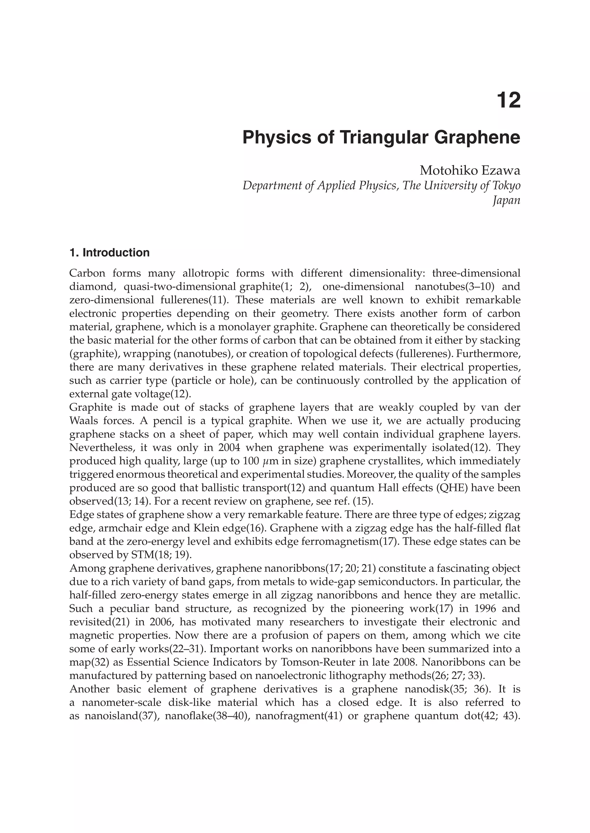
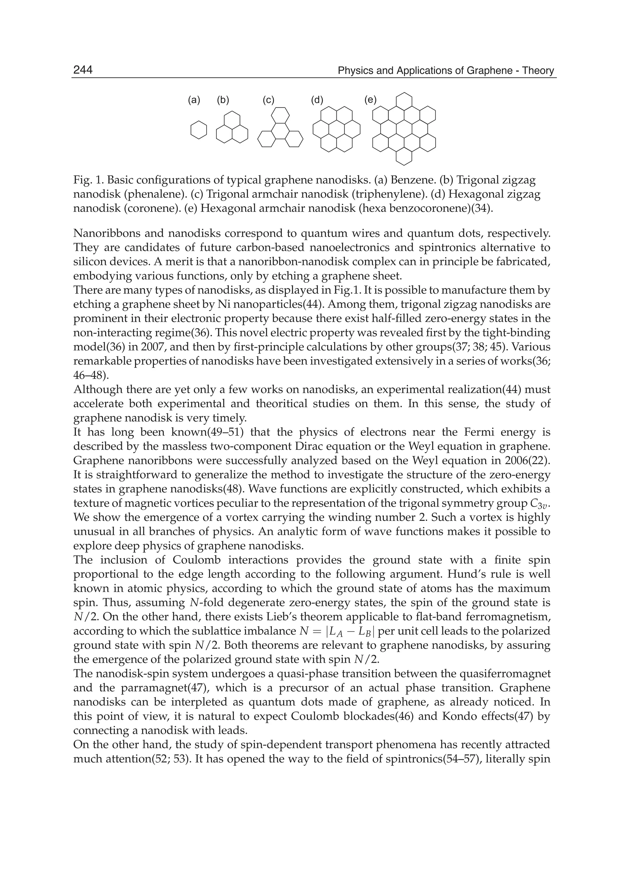
![(b) (c) (d)(a)
.
Fig. 2. (a) Key features of etching in SLG are chirality-preserving angles of 60 and 120,
avoided crossing of trenches leaving ∼10 nm spacing between adjacent trenches and
producing connected nanostructures, and trenches and nanoparticles with uniform width <
10 nm. (b) AFM phase image of etched SLG with produced geometric nanostructures. The
phase image obscures small details, making adjacent trenches appear to merge together. (c)
AFM height image of equilateral triangle connected to three nanoribbons. (d) artoon of a Ni
particle etching a graphene sheet (not to scale). Ni nanoparticles absorb carbon from
graphene edges which then reacts with H2 to create methane. These figures are taken from
the work of Campos et al. (44)
graphene (SLG) which effectively has all cuts oriented with the same edge-chirality based
on the work of Campos et al. (44). By using this method nanoribbons, equilateral triangles
(trigonal nanodisks), and other graphene nanostructures are fabricated, which could feature
novel electronic behavior resulting from their specific edge orientations.
During the high-temperature etching stage, the Ni nanoparticles etch the graphene through
catalytic hydrogenation of carbon, where carbon atoms from exposed graphene edges
dissociate into the Ni nanoparticle, and then react with H2 at the Ni surface. This process
is summarized by the chemical reaction
Ni + Cgraphene + 2H2 → Ni + CH4, (1)
where carbon from the graphene is hydrogenated into methane by the Ni nanoparticle
catalyst. The same reaction can also be understood as the effective reverse of catalytic carbon
nanotube (CNT) growth, and indeed it is found that the growth of CNTs competes with the
desired etching results in graphene. This occurs because at high concentrations of carbon
the Ni nanoparticles become supersaturated with carbon and can begin to expel carbon
nanotubes. It is for this reason that extra precaution is necessary during preparation to avoid
organic contaminants which can act as carbon sources and saturate the Ni nanoparticles.
In addition, methane produced by the etching process itself can supersaturate the Ni
nanoparticles if the amount of Ni on the substrate is too low.
The etching process produces a mosaic of clearly defined cuts across the SLG surface, as
measured by atomic force microscopy [Fig.2(b,c)]. These continuous trenches left behind by
individual nanoparticles run along straight lines, intermittently deflecting from their path
or reflecting away from previously etched trenches. These deflections and reflections show
a surprising regularity, with measured angles between any pair of trenches of either 60◦ or
120◦ [Fig. 2(a)]. Trenches forming edges at angles of 60◦ and 120◦ preserve the chirality of the
edges, indicating that nearly all the cuts in our samples run along the same crystallographic
orientation.
3. Electronic properties of nanodisks
In this section we summarize the basic nature of trigonal zigzag nanodisks(36). There exists
N-fold degenerate zero-energy states, implying that the zero-energy sector has the SU(N)
246 Physics and Applications of Graphene - Theory](https://image.slidesharecdn.com/grrphysicsandapplicationsofgraphene-theory-140422181144-phpapp02/75/physics-and_applications_of_graphene_-_theory-256-2048.jpg)
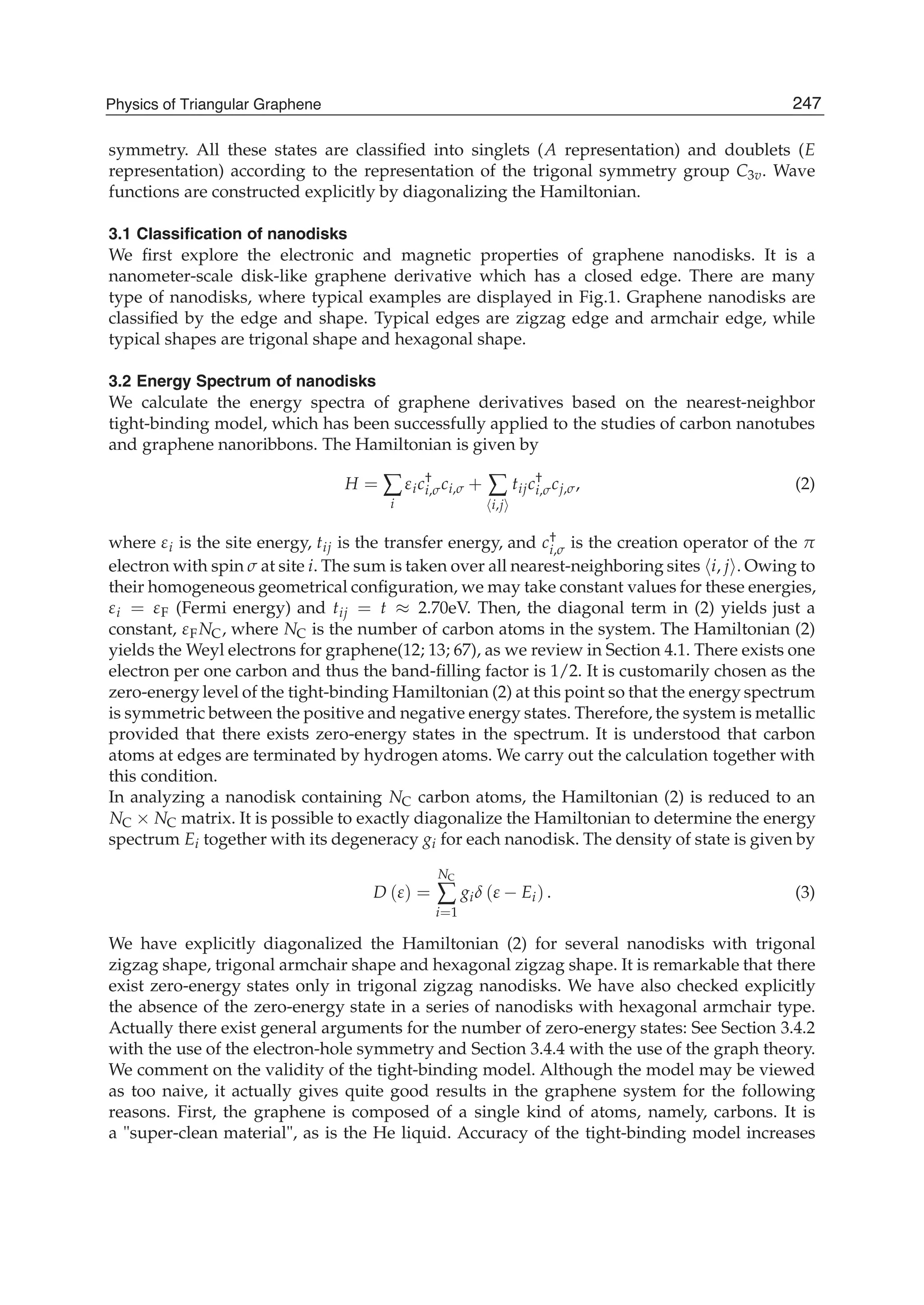
![0 1 3 5 7
0
2 4 6
-3
-2
-1
1
2
3
(b)(a) (c) E(N)E(N)
N
1 3 5 7 9 11 13
0.2
0.4
0.6
0.8
1.0
N
Fig. 3. (a) Geometric configuration of trigonal zigzag nanodisks. We define its size N by
N = Nben − 1 with Nben the number of benzenes on one side of the trigon. Here,
N = 1, 2, 3, 4, 5. The number of carbon atoms are related as NC = N2 + 6N + 6. (b) Density of
states of the N-trigonal nanodisk for N = 0, 1, 2, · · · , 7. The horizontal axis is the size N and
the vertical axis is the energy ε(N) in units of t = 2.7eV. Segments in each energy level
indicate the degeneracy of the level. (c) The excitation gap ε as a function of the size N. It is
approximately proportional to N−1.
as the number of involved elements becomes lower. For instance, it is hard to determine
the energy spectrum by the simple tight-binding model in transition metal oxides, since
it contains many elements. Second, carbon is a light element, and there are only a few
electrons in the shell. Especially in carbon there are only s and p orbitals. Furthermore, it
is possible to neglect spin-orbit couplings since they are very small. Third, the graphene
consists of the sp2 orbital and the π orbital, where sp2 orbitals contribute to make a rigid
skeleton of the graphene structure, while π orbitals spread out in graphene and behave as free
electrons. These two energy levels are well separated. Consequently, the simple tight-binding
Hamiltonian presents a very good description of the graphene system by treating π electrons
as free electrons.
3.3 Trigonal zigzag nanodisks
We shall investigate trigonal zigzag nanodisks in more details since they have zero-energy
states. We define the size N of a nanodisk by N = Nben − 1, where Nben is the number
of benzenes on one side of the trigon as in Fig.3(a). We show the density of state for N =
1, 2, · · · , 5 in Fig.3(b).
It can be shown that the determinant associated with the Hamiltonian (2) has such a factor as
det [εI − H (NC)] ∝ εN
, (4)
implying N-fold degeneracy of the zero-energy states. Since there exist half-filled zero-energy
states for N ≥ 1, these nanodisks are "metallic". The gap energy between the first-excitation
and the ground states decreases as the size becomes larger [Fig.3(c)].
3.4 Zero-energy sector
The size-N nanodisk has N-fold degenerate zero-energy states, where the gap energy is
as large as a few eV. Hence it is a good approximation to investigate the electron-electron
interaction physics only in the zero-energy sector, by projecting the system to the subspace
made of those zero-energy states. The zero-energy sector consists of N orthonormal states
| fα , α = 1, 2, · · · , N, together with the SU(N) symmetry. We can expand the wave function of
the state | fα as
fα(x) = ∑
i
ωα
i ϕi(x), (5)
248 Physics and Applications of Graphene - Theory](https://image.slidesharecdn.com/grrphysicsandapplicationsofgraphene-theory-140422181144-phpapp02/75/physics-and_applications_of_graphene_-_theory-258-2048.jpg)
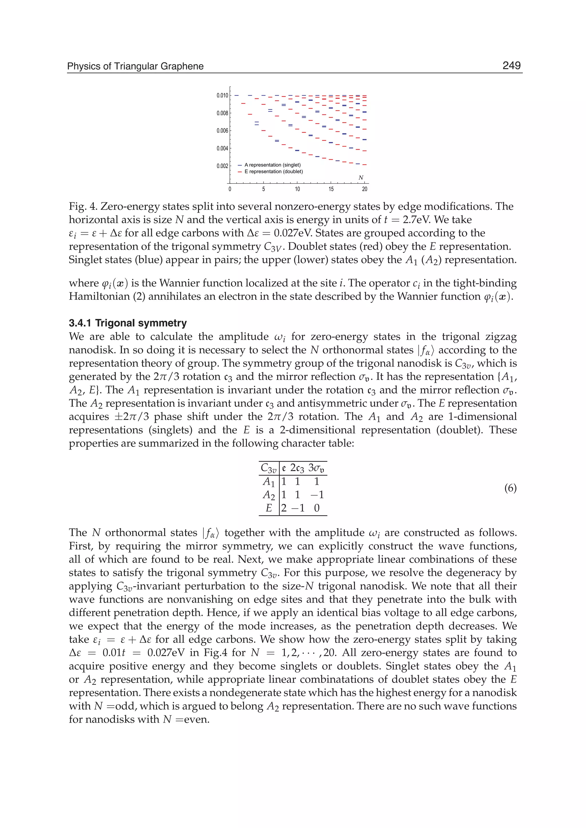
![(a) (b) (d)(c) (e)|fa> |fb> |fc> |fd> |fe>
Fig. 5. (a)∼(e) The zero-energy states of the trigonal nanodisk with size N = 5. They are
symmetric under the mirror reflection with respect to the vertical axis. The solid (open) circle
denotes the positive (negative) amplitude ωi. The amplitude is proportional to the radius of
circle. Electrons are localized on edges in the state (a). When the site energy εi is increased at
edges equally, the degeneracy is partially resolved, as illustrated in Fig.4. The state (a) has the
highest energy and is a singlet in the A2 representation of the symmetry group Cv3. The states
(b) and (c) are degenerate; the states (d) and (e) are degenerate and have the lowest energy.
Let us explain the above scheme by taking an example of the nanodisk with size N = 5.
First, we present 5 orthonormal states | fα in Fig.5, where the solid (open) circle denotes
the positive (negative) amplitude ωi with |ωi| being proportional to the radius of the
circle. Second, the wave function | fa is entirely localized on edge sites as in Fig.5(a). Since
it is invariant under the 2π/3 rotation c3 and antisymmetric under the mirror reflection
σv, it is a singlet state obeying the A2 representation. Third, we find two sets of states
(| fb , | fc ) and (| fd , | fe ) are degenerate under the C3v-invariant perturbation. Thus, we have
identified 5 states in the spectrum of Fig.4. From the mirror symmetric states we construct
the trigonal symmetric states by making a linear combination within each doublet, |g± =
1√
2
(| fb ± i| fc ), |h± = 1√
2
(| fd ± i| fe ). Each sets of complex wave functions, (|g+ , |g− )
and (|h+ , |h− ), transform properly under the E representation. We shall present an analytic
approach to investigate these states based on the Dirac theory in Section 4.3. In the instance
of N = 5, (|g+ , |g− ) and (|h+ , |h− ) correspond to (| + k+
2 , | − k+
2 ) and (| + k−
2 , | − k−
2 ),
respectively, with k±
n being defined in (38).
3.4.2 Electron-hole symmetry
We have shown that the zero-energy sector of the trigonal zigzag nanodisk has the N-fold
degeneracy by diagonalizing the Hamiltonian (2) explicitly. We wish to derive this fact from
a general point of view. First, we appeal to the electron-hole symmetry of the tight-binding
Hamiltonian (2). The Hamiltonian is invariant under the electron-hole transformation, cσ,A →
c†
σ,A, cσ,B → −c†
σ,B. As a result, the band structure is symmetric between the positive-energy
states and the negative-energy states, as is explicitly seen in Fig.3(b). The number of the
positive-energy state ν+ and the negative-energy state ν− are equal ν+ = ν−. On the other
hand, the number of the total states is equal to the number of carbon atoms, NC = N2 + 6N +
6. Hence, the number of the zero-enegy state η is given by η = NC − ν+ − ν−. Now, the number
of the positive or negative-energy state is less than 2 min [NA, NB], ν± ≤ 2 min [NA, NB], where
NA and NB are the numbers of sites in sublattices A and B, respectively [see Fig.6]. We obtain
η ≥ |NA − NB|. It is easy to see NA = (N + 1)(N + 6)/2, NB = (N + 2)(N + 3)/2 for the
trigonal zigzag nanodisk, and hence η ≥ N for the size-N nanodisk.
3.4.3 Bipartite lattice
We have derived the lower limit for the dimension of the zero-energy sector, η ≥ N. It is a
characteristic feature of the tight-binding Hamiltonian on the bipartite lattice that it can be
250 Physics and Applications of Graphene - Theory](https://image.slidesharecdn.com/grrphysicsandapplicationsofgraphene-theory-140422181144-phpapp02/75/physics-and_applications_of_graphene_-_theory-260-2048.jpg)
![B-siteA-site
●
●
A
B
A
B
A
B
A
B
A
B
A
B
a1
a2
(a) (b) (c)
Fig. 6. (a) The two-dimensional honeycomb lattice is made of two trigonal sublattices
generated by the two basis vectors a1 and a2 from the two base points A and B in primitive
cell (dotted rectangle). (b,c) The A-sites and B-sites of a trigonal nanodisk. Electrons exist
only in A sites.
represented in the form of
H =
0 TAB
TBA 0
. (7)
The wave function is decomposed into two parts describing the A sites and B sites, |f =
( fA, fB)t
. The rank of the matrix (7) is 2NB at the highest, but it is 2NB for connected lattices.
As a result the number of the zero-energy eigenvalues of the (NA + NB)-dimensional matrix
(7) is given by η = NA − NB = N, where the last equality holds for the zigzag trigonal
nanodisk with (??).
Furthermore, we are able to show that the wave function takes a nonzero value only on the
A-site. The matrix TBA is NB × NA dimensional. Let us choose NA-dimensional eigenvectors
satisfying TBA | fA = 0. The number of such eigenvectors is N = NA − NB > 0, as we have
just shown. We now consider the (NA + NB)-dimensional vector, | fA = ( fA, 0)t
. It is trivial
to see that it is the eigenvector of H, H | fA = (0, TBA fA)t
= 0. We have proved that there are
N zero-energy eigenvalues whose wave functions vanish on all B sites. See Fig.5 and Fig.6.
3.4.4 Graph theory
There is another way to see the dimension of the zero-energy sector. The spectrum of the
tight binding Hamiltonian of a honeycomb system can also be analyzed on the basis of a
mathematically rigorous approach of the benzenoid graph theory(68). According to this graph
theory, the number of zero-energy states is equal to the graph’s nullity, η = 2α − NC, where
NC is the total number of sites and α is the maximum number of non-adjacent sites. Here, we
have η = N, since α = NA for the trigonal zigzag nanodisk [Fig.6].
3.5 Robustness against randomness and lattice defects
In actual application, however, it is important to discuss how stable the previous results are
against lattice defects and randomness in transfer energy. We study three types of randomness:
randomness in transfer energy, randomness in site energy and lattice defects. The modified
Hamiltonian is
H0 = ∑
i
(εi + δεi) c†
i,σci,σ + ∑
i,j
tij + δtij c†
i,σcj,σ, (8)
where we take random values for δεi and δtij.
First of all the total spin of the ground state is determined by Lieb’s theorem although transfer
randomness and lattice defects are included. (See Section 5.5 for Lieb’s theorem.) The total
251Physics of Triangular Graphene](https://image.slidesharecdn.com/grrphysicsandapplicationsofgraphene-theory-140422181144-phpapp02/75/physics-and_applications_of_graphene_-_theory-261-2048.jpg)
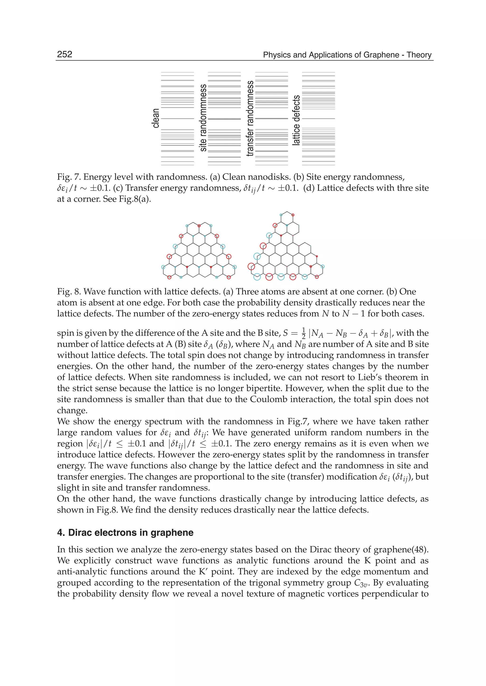
![the nanodisk plane. It is intriguing that a vortex with the winding number 2 emerges in the
state belonging to the E (doublet) representation.
4.1 Weyl equations
Electrons obey the massless two-component Dirac equation, or the Weyl equation, in
graphene(49–51). We start with a review how Dirac electrons arise from the one-particle
electronic states in the honeycomb lattice [Fig.9]. We take the basis vectors a1 and a2 as
a1 = (1, 0) a, a2 = 1/2,
√
3/2 a, with a the lattice constant (a ≈ 2.46Å). The honeycomb
lattice has two different atoms per primitive cell, which we call the A and B sites. There
are three B sites adjacent to an A site, which are specified by the three vectors ri with
r1 = 0, −1/
√
3 a, r2 = 1/2, 1/ 2
√
3 a, r3 = −1/2, 1/ 2
√
3 a. The basis vectors bi
of the reciprocal lattice are given by solving the relations bi · aj = 2πδij. The Brillouin zone is
a hexagon in the reciprocal lattice with opposite sides identified.
We rewrite the tight-binding Hamiltonian (2) as
H = t ∑
x,i
c†
A (x) cB (x + ri) + c†
B (x + ri) cA (x) , (9)
where cS and c†
S are the annihilation and creation operators for electrons localized at the S site
(S =A,B). It describes a transfer of an electron between neighboring A and B sites without
changing its spin. We introduce the Fourier transform of the electron annihilation operator
cS (x),
cS (x) =
d2k
2π
eik·x
cS (k) . (10)
The Hamiltonian (9) reads
H = t d2
k c†
A, c†
B
0 f (k)
f ∗ (k) 0
cA
cB
(11)
in the momentum space, where
f (k) = e−ikya/
√
3
+ 2eikya/2
√
3
cos
kxa
2
. (12)
●
●
● ●
A
K
K
K’
K’
B
A
A
B
A
B
A
A
B
a1
b2
ky
kx
b1
a2
x
(a) (b)
Fig. 9. (a) The two-dimensional honeycomb lattice is made of two triangular sublattices
generated by the two basis vectors a1 and a2 from the base points A and B in a primitive cell
(a dotted rectangle in yellow). (b) The reciplocal lattice is also a honeycomb lattice with the
basis vectors b1 and b2. We take the Brillouin zone as indicated by a dotted rectangle in
yellow. As two inequivalent points we take K and K’ as indicated.
253Physics of Triangular Graphene](https://image.slidesharecdn.com/grrphysicsandapplicationsofgraphene-theory-140422181144-phpapp02/75/physics-and_applications_of_graphene_-_theory-263-2048.jpg)
![9 eV
- 9 eV
0 eV
1.5 eV
E
ky
kx
K’
K
(a) (b)
Fig. 10. (a) The overall valley structure of the dispersion relation (13) is illustrated. (b) A
schematic diagram of the low-energy dispersion relation (13) near the Dirac points (K and K’
points) in the Brillouin zone. Only two Dirac cones are inequivalent to one another.
● ●
K K K
K
K’
K’
K’
ky
kx
(b)(a) (c)
(b)
(c)
1 2 3 3.02.51.50.5-3 -2 -1
9eV
-9eV
6eV
-6eV
3eV
-3eV
9eV
-9eV
6eV
-6eV
3eV
-3eV
Fig. 11. Linear dispersion near the Brillouin zone corner. The linear region of the band is
found to be dependent on the direction in the k space. In one of the direction (c) the linearity
is good more than 3 eV.
The eigenvalues are found to be ±E (k) with
E (k) = t 1 + 4 cos
√
3kya
2
cos
kxa
2
+ 4 cos2 kxa
2
. (13)
The dispersion relation (13) implies that the Fermi level at E (k) = 0 is reached by six corners
of the first Brillouin zone, among which there are only two inequivalent points due to the
periodicity of the reciprocal lattice. We take them as
K+
= 2π/3, 2π/
√
3 /a, K−
= −2π/3, 2π/
√
3 /a, (14)
and call them the K and K’ points [Fig.9(b) and Fig.10]. They endow graphene with a
two-component structure, corresponding to two independent Fermi points. It is notable that
the dispersion relation (13) has a valley structure around the K and K’ points.
The band dispersion (13) is linear in these Dirac valleys [Fig.10],
Eκ (k) = ¯hvF|k − Kτ
| for k Kτ
, (15)
where τ = ± is the valley index and vF =
√
3ta/ (2¯h) is the Fermi velocity. We show two
sections of the band in Fig.11, where the linear region of the band is found to be dependent
on the direction in the k space. In one of the section the linearity prevails more than 3 eV, as
in Fig.11(c). This linear behavior has been confirmed experimentally(69) up to 3eV.
We may expand f (x) as
f (x)
(−1)−1/3
√
3
2
τ (kx − Kτ
) − i ky − Kτ
(16)
254 Physics and Applications of Graphene - Theory](https://image.slidesharecdn.com/grrphysicsandapplicationsofgraphene-theory-140422181144-phpapp02/75/physics-and_applications_of_graphene_-_theory-264-2048.jpg)
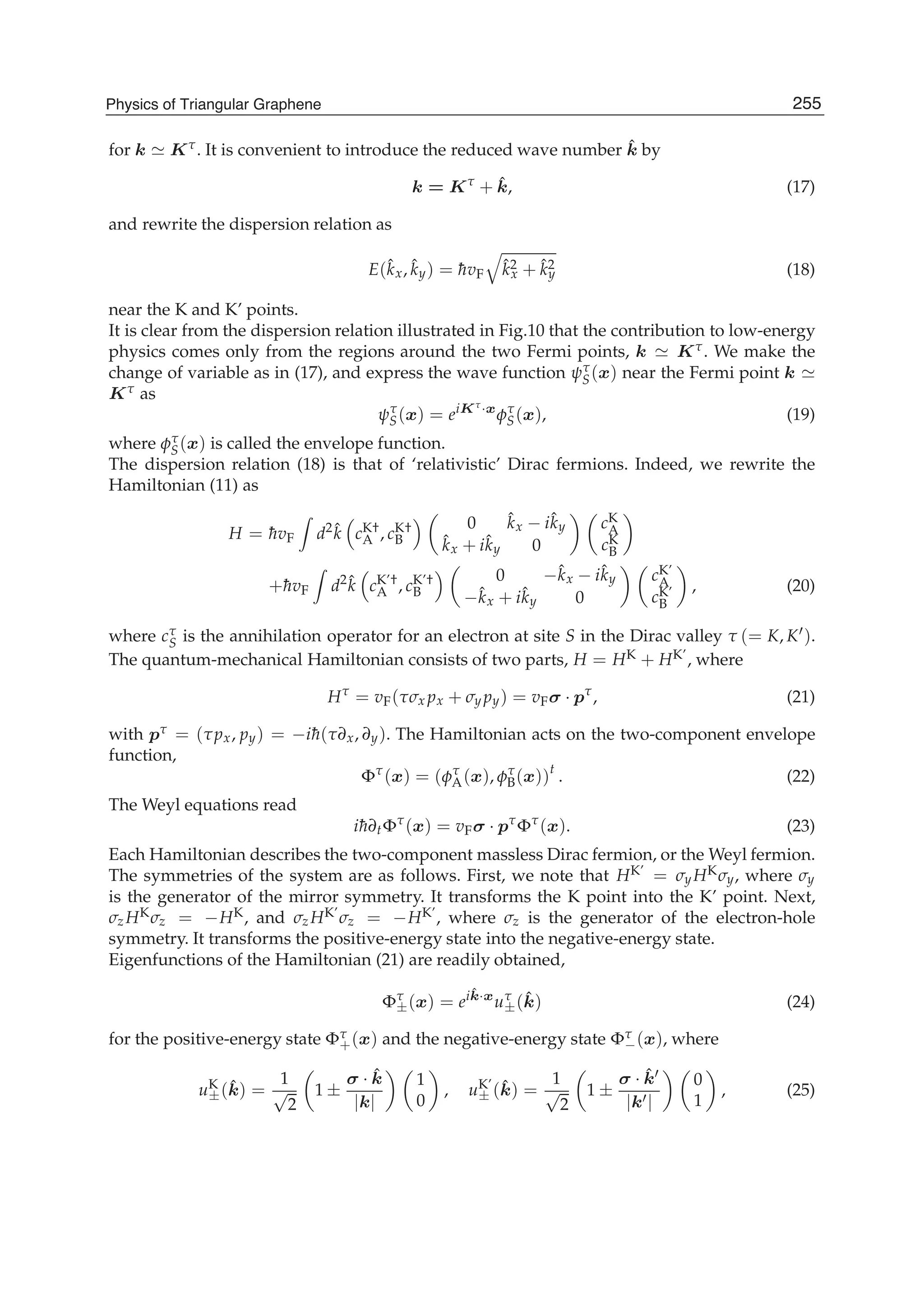
![● ● ●● ●●
●
●
●
●
●
●
●
●
●
●
●
●
Fig. 12. The electron density is found to be localized along the edges of a trigonal nanodisk.
in terms of the original wave number k, or
−
π
3
≤ aˆk < 0 and 0 < aˆk ≤
π
3
, (33)
in terms of the reduced wave number ˆk, around the K’ and K points, respectively. The
boundary point ak = −π of the K’ point is simultaneously the boundary point ak = π of
the K point in another Brillian zone, as illustrated in Fig.13: They are physically the same
point and to be identified.
4.3 Dirac electrons in triangular Graphene
Our main purpose is to apply the above result to the analysis of the zero-energy sector of
the trigonal zigzag nanodisk [Fig.12]. The envelope function of the trigonal zigzag nanodisk
can be constructed by making a linear combination of envelope functions for three trigonal
corners. We consider the trigonal region whose corners are located at z1 = (L, 0), z2 = (−L, 0),
z3 = 0,
√
3L . As the boundary conditions we impose φ (z1) = φ (z2) = φ (z3) = 0. The
resultant envelope function is obtained around the K point (ˆk > 0) as
φ (z) = eiˆkz
− eiˆkL
eiˆk(z−L)exp[−2πi/3] − e−iˆkL
eiˆk(z+L)exp[2πi/3] (34)
up to a normalization constant. The envelope function around the K’ point (ˆk < 0) is given by
φ (z∗). We display the density of the wave function |φ (z)|2
in Fig.12.
The wave number is quantized for a finite edge such as in the trigonal nanodisk. We can
determine it as follows. We focus on the wave function ψτ
A (x) at one of the A sites on an
edge. There are N links along one edge of the size-N trigonal nanodisk. We can show that
the correction terms are exactly cancelled out for these N links, and we obtain precisely
Θτ(a/2, N) = Nak. On the other hand, the phase shift is π at the corner. The total phase
shift is 3Nak + 3π, when we encircle the nanodisk once. For the single-valueness of the wave
function it is necessary that 3Nak + 3π = 2nπ, or
ˆkn = ±
(2n + 1) π
3Na
, 0 ≤ n ≤
N − 1
2
, (35)
with an integer n. The allowed region of the wave number is given by (32). The wave number
is quantized as
kn = ±
2n + 1
3N
+
2
3
π
a
, 0 ≤ n ≤
N − 1
2
. (36)
When N is even, there are N/2 states for kn > 0 and N/2 states for kn < 0. When N is odd,
there are (N − 1)/2 states for kn > 0 and (N − 1)/2 states for kn < 0. Additionally, there seem
257Physics of Triangular Graphene](https://image.slidesharecdn.com/grrphysicsandapplicationsofgraphene-theory-140422181144-phpapp02/75/physics-and_applications_of_graphene_-_theory-267-2048.jpg)
![kx
kx
ky
Energy Level
K
K
K
K’
K’
K’
p-p
(a)
(b)
Fig. 13. (a) The energy spectrum in an infinitely long graphene edge. The flat band appears in
the region indicated in red. (b) We take the Brillouin zone as indicated in yellow. The flat
band appears in the region indicated in red. The boundary points at ±π are identified.
to appear two states with kn = ±π/a at n = (N − 1)/2. However, they are identified with
one another, since they are located at the boundary of the Brillouin zone [13].
As we have reviewed in Section 3.4, the symmetry group of the trigonal nanodisk is C3v,
whose properties are summarized in the table (6). The mirror symmetry is equivalent to the
exchange of the K and K’ points. With respect to the rotation there are three elements c0
3, c3,
c2
3, which correspond to 1, e2πi/3, e4πi/3. Accordingly, the phase shift of one edge is 0, 2π/3,
4π/3. They are determined by the conditions
Nakn + π = 2nπ, Nakn + π = 2nπ +
2π
3
, Nakn + π = 2nπ +
4π
3
, (37a)
with an integer n, respectively. It follows that the state, indexed by the edge momentum kn
as in (36), are grouped according to the representation of the trigonal symmetry group C3v as
follows,
A1 (singlet) : |k0
n + | − k0
n ,
A2 (singlet) : |k0
n − | − k0
n ,
k0
n =
6n + 3
3Na
π,
E (doublet) : |k±
n , | − k±
n , k±
n =
6n ± 1
3Na
π,
(38)
where the momentum kα
n is subject to the condition (32). It follows that
N + 1
3
≤ n ≤
N
2
, (39)
where a denotes the maximum integer equal to or smaller than a, and a denotes the
minimum integer equal to or larger than a. The numbers of doublets (E-mode) and singlets
(A1-mode or A2-mode) are given by
N + 1
3
, N − 2
N + 1
3
, (40)
respectively.
258 Physics and Applications of Graphene - Theory](https://image.slidesharecdn.com/grrphysicsandapplicationsofgraphene-theory-140422181144-phpapp02/75/physics-and_applications_of_graphene_-_theory-268-2048.jpg)
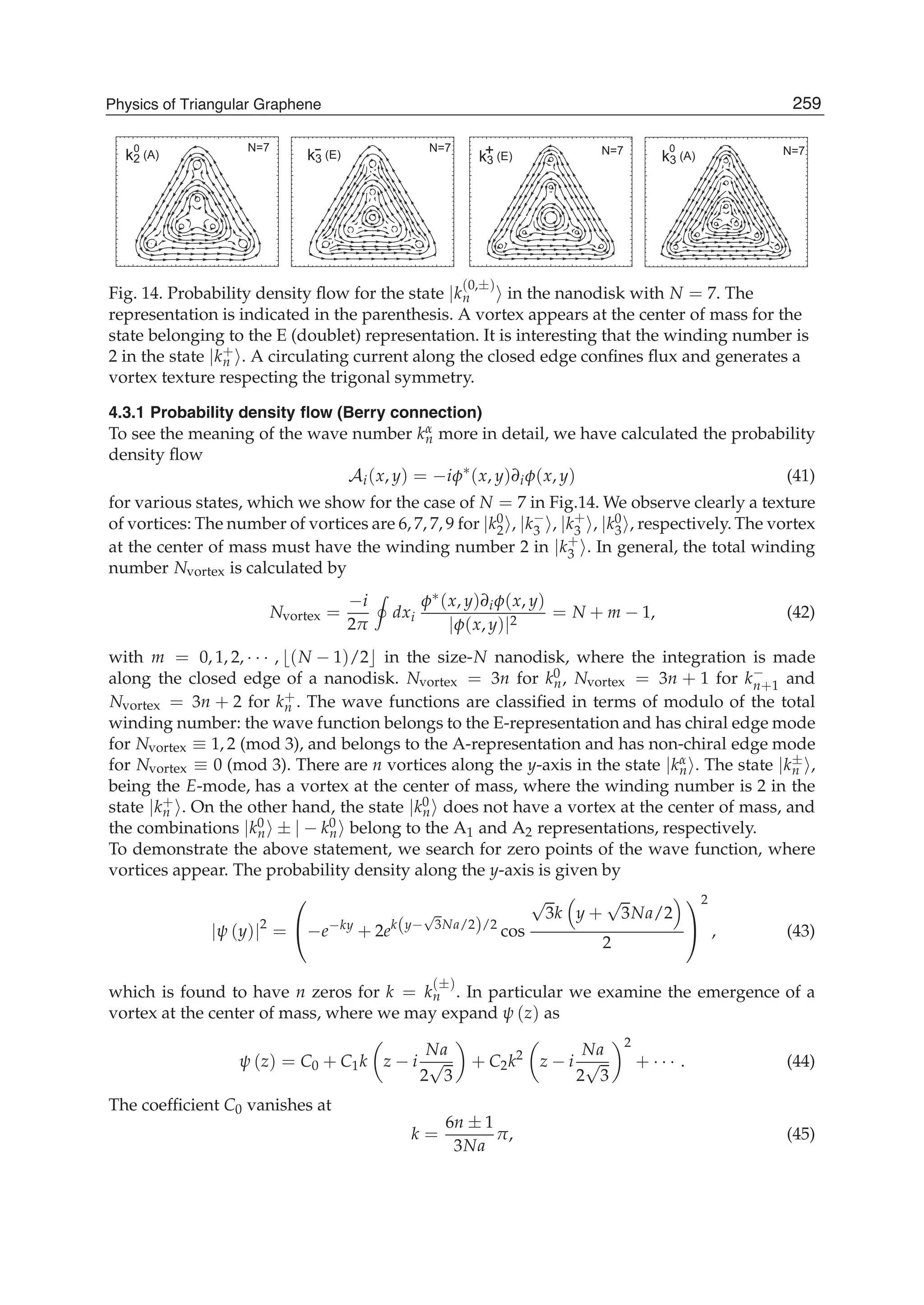
![which means that a nanodisk is a rigid ferromagnet. The system is well described by
the infinite-range Heisenberg model, which is exactly solvable. Constructing the partition
function, we explore thermodynamical properties(47; 65). A sharp peak emerges at a certain
temperature in the specific heat, which we interpret as a quasi-phase transition between
quasiferromagnetic and paramagnetic states.
5.1 Exchange interactions
Let us include the Coulomb interaction between electrons in the zero-energy sector. We take
two states | fα and | fβ , α = β, each of which can accommodate two electrons with up and
down spins at most. The two-state system is decomposed into the spin singlet χS and the spin
triplet χT with the normalized wave functions,
fSS
αβ(x, x ) =
1
√
2
fα(x) fβ(x ) + fα(x ) fβ(x) χS, (49a)
fST
αβ (x, x ) =
1
√
2
fα(x) fβ(x ) − fα(x ) fβ(x) χT. (49b)
The Coulomb energies are summarized as
f SS
αβ|HC| f SS
αβ = Uαβ + Jαβ, f ST
αβ |HC| f ST
αβ = Uαβ − Jαβ, (50)
where Uαβ and Jαβ are the direct and exchange energies. In the many-state system the effective
Hamiltonian is derived as
HD = ∑
α≥β
Uαβn (α) n (β) −
1
2 ∑
α>β
Jαβ[4S(α) · S(β) + n (α) n (β)], (51)
where n (α) = d†
σ(α)dσ(α) is the number operator and S(α) = 1
2 d†
σ(α)τσσ dσ (α) is the spin
operator, with dσ(α) the annihilation operator of electron with spin σ =↑, ↓ in the zero-energy
state | fα : τ is the Pauli matrix. Note the existence of the on-state Coulomb term Uααn (α) n (α)
in the effective Hamiltonian (51).
We expand Uαβ and Jαβ in terms of the Wannier functions with the use of (5),
Uαβ = ∑
s
ωα
i ωα
j ω
β
k ω
β
l d3
xd3
y ϕ∗
i (x)ϕj(x)V(x − y)ϕ∗
k (y)ϕl(y), (52a)
Jαβ = ∑
s
ωα
i ωα
j ω
β
k ω
β
l d3
xd3
y ϕ∗
i (x)ϕj(y)V(x − y)ϕ∗
k (y)ϕl(x). (52b)
The dominant contributions come from the on-site Coulomb terms with i = j = k = l both for
the direct and exchange energies. We thus obtain
Uαβ Jαβ U ∑
i
(ωα
i ω
β
i )2
, (53)
with
U ≡
e2
4πε
d3
xd3
y ϕ∗
i (x)ϕi(x)
1
|x − y|
ϕ∗
i (y)ϕi(y). (54)
The Coulomb energy U is of the order of 1eV because the lattice spacing of the carbon atoms is
∼ 1Å in graphene. The nearest neighbor Coulomb interaction vanishes since no electrons exist
in B sites: See Fig.6. It is straightforward to take into account higher order corrections but the
effects are only to enhance the ferromagnetic order. The essential properties of the Coulomb
interactions are well described only by taking the on-site terms.
261Physics of Triangular Graphene](https://image.slidesharecdn.com/grrphysicsandapplicationsofgraphene-theory-140422181144-phpapp02/75/physics-and_applications_of_graphene_-_theory-271-2048.jpg)
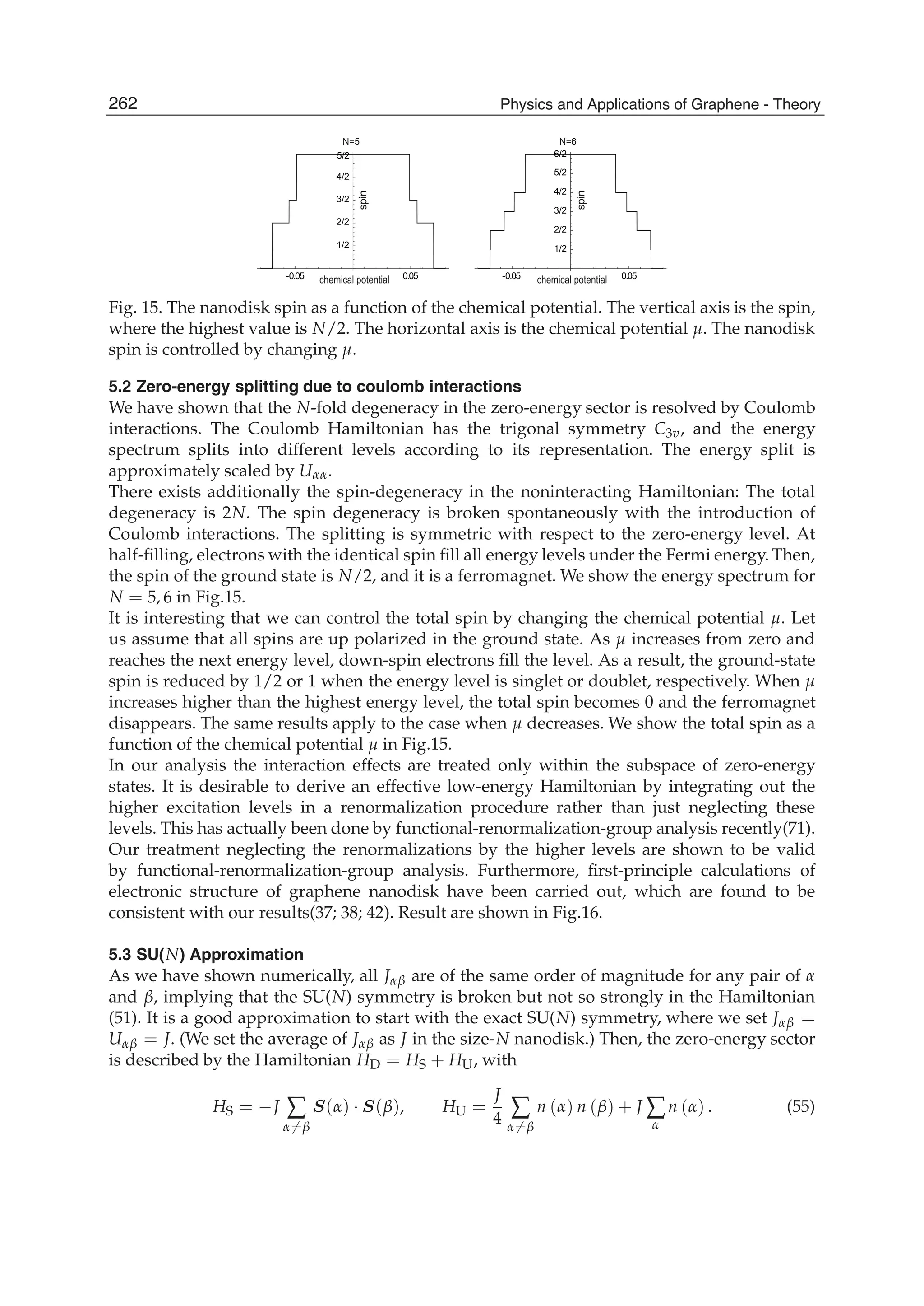
![(a) (b) (c)
080604
0
2
4 TB+HF
TB
DFT
Energy[eV]
Eigenstate index
TB+HF DFT
DFTTB+HF
dgate
(a)
(b)
Gate charge
Graphene island
Fig. 16. The first-principle calculation of graphene nanodisdks. Fig. (a) is taken from the work
of Fernández-Rossier et. al (37), Fig. (b) is taken from the work of Wang et. al (38) and Fig. (c)
is taken form the work of Güçlü et al.(42).
The term HS is known as the infinite-range Heisenberg model. We rewrite them as
HS = −JS2
tot +
3
4
Jntot, HU =
J
4
(n2
tot + 1), (56)
where ntot = ∑α n (α) is the total electron number.
The ground states of nanodisks are half filled. We restrict the Hilbert space to the half-filling
sector, where n (α) = n↑ (α) + n↓ (α) = 1. The Hamiltonian (56) is reduced to the Heisenberg
model,
HS = −JStot · Stot, (57)
where we have neglected an irrelevant constant term, (3/4)JN. This is exactly diagonalizable,
HS|Ψ = Es|Ψ , with Es = −Js(s + 1), where s takes values from N/2 down to 1/2 or 0,
depending on whether N is odd or even, s = N
2 , N
2 − 1, N
2 − 2, · · · , s ≥ 0. The Hilbert
space is diagonalized, H = ⊗NH1/2 = ⊕gN(s)Hs, where Hs denotes the (2s + 1) dimensional
Hilbert space associate with an irreducible representation of SU(2). The multiplicities gN (s)
satisfies the recursion relation coming from the spin synthesizing rule, gN (s) = gN−1(s −
1
2 ) + gN−1(s + 1
2 ). We solve this as gN(1
2 N − q) =N Cq −NCq−1. The total degeneracy of the
energy level Es is (2s + 1) gN(s). At half filling, the eigenstate of the Hamiltonian HD is labeled
as |Ψ = |ntot, s, m , where s is the total spin and m is its z-component.
5.4 Thermodynamical properties
We have a complete set of the eigenenergies together with their degeneracies. The partition
function of the nanodisk with size N is exactly calculable(47). According to the standard
procedure we can evaluate the specific heat C(T), the entropy S(T), the magnetization
S2
tot and the susceptibility χ = S2
z,tot − Sz,tot
2
/ (kBT)from this partition function.
The ground-state value of the total spin is Sg = (N/2) (N/2 + 1). The entropy is given
by S (0) = kB log(N + 1) at zero temperature. We display them in Fig.17 for size N =
1, 2, 22, · · · 210.
There appear singularities in thermodynamical quantities as N → ∞, which represent a phase
transition at Tc between the ferromagnet and paramagnet states, Tc = JN/ (2kB). For finite
263Physics of Triangular Graphene](https://image.slidesharecdn.com/grrphysicsandapplicationsofgraphene-theory-140422181144-phpapp02/75/physics-and_applications_of_graphene_-_theory-273-2048.jpg)
![(a) (c)
(d)(b)
1.0
0.8
0.6
0.4
0.2
4
3
2
1
1.0
0.8
0.6
0.4
0.2
1.0
1.2
0.8
0.6
0.4
0.2
0.2 0.4 0.6 0.8 1.0
0.2 0.4 0.6 0.8 1.0 0.2 0.4 0.6 0.8 1.0
Tc
Specificheat(C/kBN)Entropy(S/kBNlog2)
Magnetization(/Sg)
Susceptibility(c/Sg)
2
S2
tot
Temperature (T/(JN/kB))
0.2 0.4 0.6 0.8 1.0
Temperature (T/(JN/kB))
1
1
2
2
1
1
4
4
8
8
4
2
8
4
16
16
16
16 64
32
256
10241024
1024
1024
1024
Fig. 17. Thermodynamical properties of the nanodisk-spin system. (a) The specific heat C in
unit of kBN. (b) The entropy S in unit of kBN log 2. (c) The magnetization S2
tot in unit of S2
g.
(d) The susceptibility χ in unit of Sg. The size is N = 1, 2, 22, · · · 210. The horizontal axis
stands for the temperature T in unit of JN/kB. The arrow represents the phase transition
point Tc in the limit N → ∞.
N, there are steep changes around Tc, though they are not singularities. It is not a phase
transition. However, it would be reasonable to call it a quasi-phase transition between the
quasiferromagnet and paramagnet states. Such a quasi-phase transition is manifest even in
finite systems with N = 100 ∼ 1000.
The specific heat and the magnetization take nonzero-values for T > Tc [Fig.17(a),(c)], which
is zero in the limit N → ∞. The entropy for T > Tc is lower than that of the paramagnet
[Fig.17(b)]. These results indicate the existence of some correlations in the paramagnet state.
As shown in Fig.17(d), the susceptibility χ always shows the Curie-Weiss low χ ∝ 1/T near
T = 0, and exhibits also a behavior showing a quasi-phase transition at T = Tc. In the
finite system, the expectation value of Sz,tot is always zero because there is no spontaneous
symmetry breakdown in the finite system, and the behavior is that of paramagnet.
5.5 Lieb’s theorem
We make some remarkable observations on the spin of a nanodisk. Due to the exchange
interaction in the Hamiltonian (51), all spins are spontaneously polarized into a single
direction. Since the exchange energy is as large as the direct energy, which is the order of a
few hundred meV, the spin stiffness Jαβ is quite large, implying that nanodisks are almost
rigid ferromagnets. We refer to the total spin of a nanodisk, Stot = ∑α S (α), as the nanodisk
spin. The size-N nanodisk spin is 1
2 N in the ground state.
This is consistent with Lieb’s theorem(72) valid for the Hubbard model. As far as only
the on-site Coulomb interactions are taken into account, the electron-electron interaction is
approximated by the Hubbard model,
HU = U ∑
i
d†
i↑di↑d†
i↓di↓, (58)
where U is given by (54): It is estimated(73) that U ≈ t. Lieb’s theorem states that, in the case
of repulsive electron-electron interactions (U > 0), a bipartite system at half-filling has the
ground state whose total spin is Stot = 1
2 |NA − NB|, where NA and NB are the numbers of
264 Physics and Applications of Graphene - Theory](https://image.slidesharecdn.com/grrphysicsandapplicationsofgraphene-theory-140422181144-phpapp02/75/physics-and_applications_of_graphene_-_theory-274-2048.jpg)
![sites in sublattices A and B, respectively [Fig.6]. They are given by (??), and hence Stot = 1
2 N
for the size-N nanodisk.
6. Large size triangular graphene
In this appendix we argue that our analysis based on the zero-energy sector is essentially
correct, even if the size N of the nanodisk is large and the band gap becomes very narrow.
In this case, the DOS of the nanodisk is decomposed into the DOS due to the edge, which is
δ-function like, and the DOS due to the bulk, which is almost continuous. The correction to
the magnetization from the bulk part is shown to be of the order of 1/N with respect to the
one from the edge part in the zero-temperature limit.
6.1 Density of states
It is possible to derive an analytical expression for the density of states of graphene per unit
cell(74), which has the form
ρ (ε) =
4
π2
|ε|
t2
1
√
Z0
K
Z1
Z0
, (59)
with
Z0 = 1 + ε
t
2
− (ε/t)2
− 1
2
/4; −t ≤ ε ≤ t
4 |ε/t| ; −3t ≤ ε ≤ −t ∨ t ≤ ε ≤ 3t
, (60a)
Z1 =
4 |ε/t| ; −t ≤ ε ≤ t
1 + ε
t
2
− (ε/t)2
− 1
2
/4; −3t ≤ ε ≤ −t ∨ t ≤ ε ≤ 3t
, (60b)
where K (x) is the complete elliptic integral of the first kind. Thus, near the Dirac point we
find
ρ (ε) =
2Ac
πv2
F
|ε| , (61)
where Ac is the unit cell area, Ac = 3
√
3a2/2.
For large N nanodisks, the band gap decreases inversely proportional to the size. One may
wonder if our analysis based on only the zero-energy sector is relevant. Indeed, the size of
experimentally available nanodisks is as large as N = 100 ∼ 1000. We would like to argue
that our analysis of the zigzag trigonal nanodisk captures the basic nature of nanodisks even
for such a large size system.
It is important to remark that each energy level is at most two-fold degenerate except for the
states at ε = 0 and ε = t irrespective to its size N, as illustrated in Fig.18. The degeneracy is
governed by the representation (6) of the trigonal symmetry group C3v. Hence, in the limit
N → ∞, the density of state (DOS) of the zigzag trigonal nanodisk reflects the following two
aspects; one is that there appear van-Hove singularities at ε = 0 and ε = t. The other is
that the DOS shows a continuous and dense structure, which has the same structure of the
bulk graphene [Fig.18] except for the contributions from these singularities. Namely, near the
Fermi energy, the DOS consists of that of the bulk graphene and an additional peak at the
zero-energy states due to the edge states for N 1, as illustrated in Fig.18. Hence, together
with spin degrees of freedom, it behaves as
D (ε) = 2cNc |ε| + 2Nδ (ε) , (62)
265Physics of Triangular Graphene](https://image.slidesharecdn.com/grrphysicsandapplicationsofgraphene-theory-140422181144-phpapp02/75/physics-and_applications_of_graphene_-_theory-275-2048.jpg)
![-3 0 3 -3 0 3-3 0 3
D(E) D(E) D(E)
E E
(a) (b) (c)
Fig. 18. The density of state of a (a) graphene, (b) graphene nanoribbon and (c) graphene
nanodisk. The horizontal axis is the energy ε.
with c = 2Ac/πv2
F. The linear term is due to the bulk states as given by (61), and the Dirac
delta function term is due to the edge states. The important point is that the edge-state peak
is clearly distinguished from the DOS due to the bulk part. It is enough to take into account
only the zero-energy sector to analyze physics near the Fermi energy, since the contribution
from the edge states is dominant.
6.2 Magnetism
For definiteness we explicitly calculate the magnetization of a nanodisk when its size is large.
We start with the Hubbard Hamiltonian,
H = ∑
ijσ
tijc†
iσciσ + U ∑
i
c†
i↑ci↑c†
i↓ci↓ = ∑
kσ
ε (k) c†
kσckσ + U ∑
kk q
c†
k+q↑c†
k −q↓ck ↓ck↑. (63)
In the Hartree-Fock approximation the Hamiltonian is transformed into
HMF = ∑ εk +
U
2NC
n + σΔ c†
kσckσ − NCU n↑ n↓ ,
where NC = N2 + 6N + 6,
Δ =
U
2NC
m +
h
2
, (64)
with the external magnetic field h and nσ = 1
2 ( n + σ m ), or n = n↑ + n↓ , m =
n↑ − n↓ . The statistical mean values n and m are determined self-consistently as
n = dερ (ε) [f (ε − Δ) + f (ε + Δ)] , (65)
m = dερ (ε) [f (ε − Δ) − f (ε + Δ)] , (66)
with the Fermi distribution function f (x) = 1/ (exp [(x − μ) /kBT] + 1). We can rewrite (66)
into
m = dερ (ε) tanh
β (ε + Δ)
2
− tanh
β (ε − Δ)
2
. (67)
Substituting the formula (62) of the DOS into the Storner equation (66), we obtain
m = N tanh
βΔ
2
+ cNc Δ2
+
1
β2
π2
3
+ 4Li2 −e−βΔ
, (68)
with the dilogarithm function Li2 (x). It is difficult to solve this equation for m
self-consistently at general temperature T. We examine two limits, T → 0 and T → ∞.
266 Physics and Applications of Graphene - Theory](https://image.slidesharecdn.com/grrphysicsandapplicationsofgraphene-theory-140422181144-phpapp02/75/physics-and_applications_of_graphene_-_theory-276-2048.jpg)
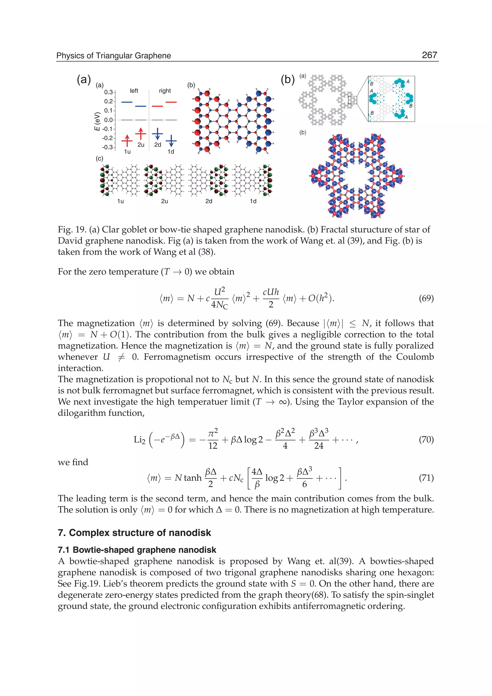
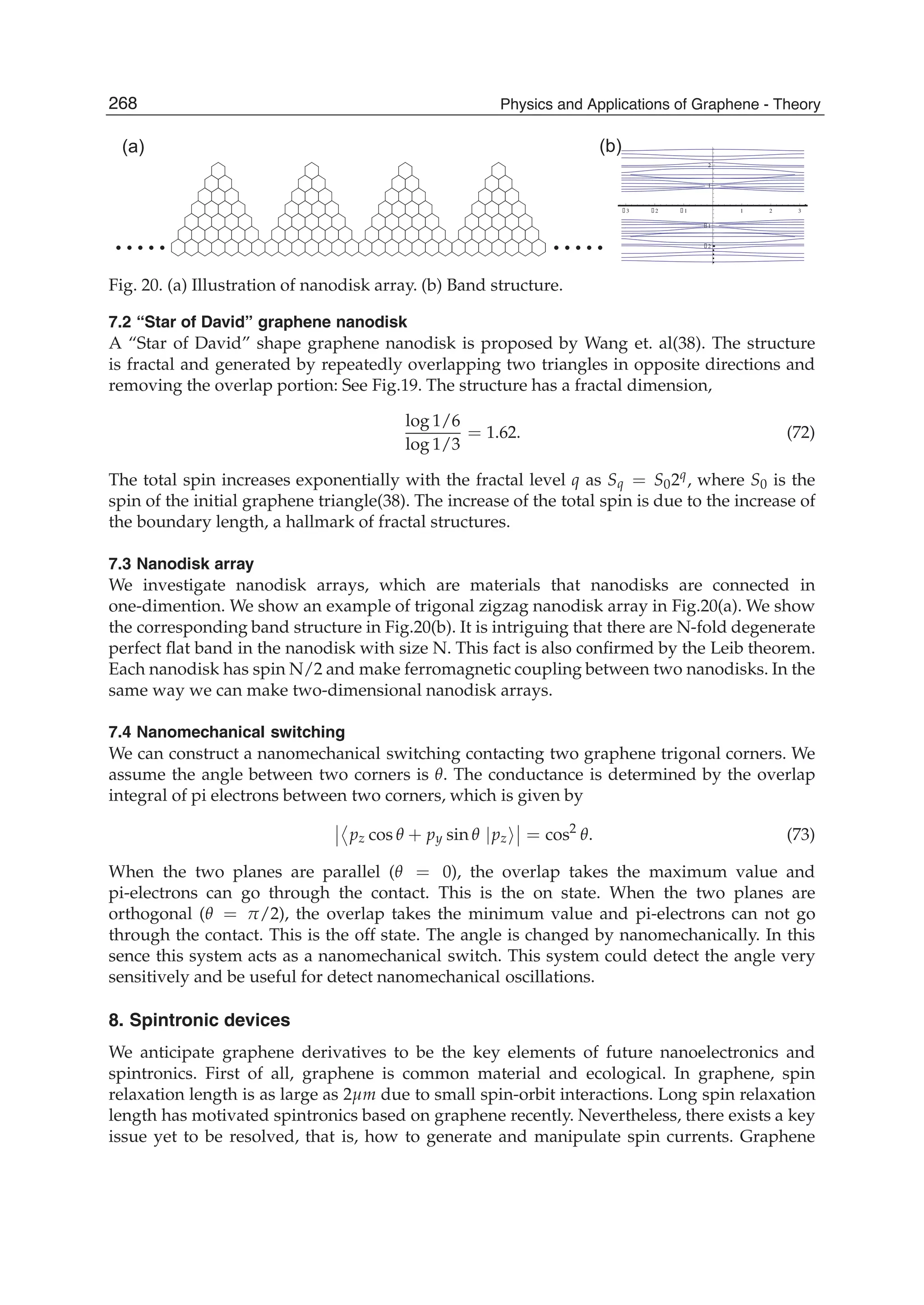
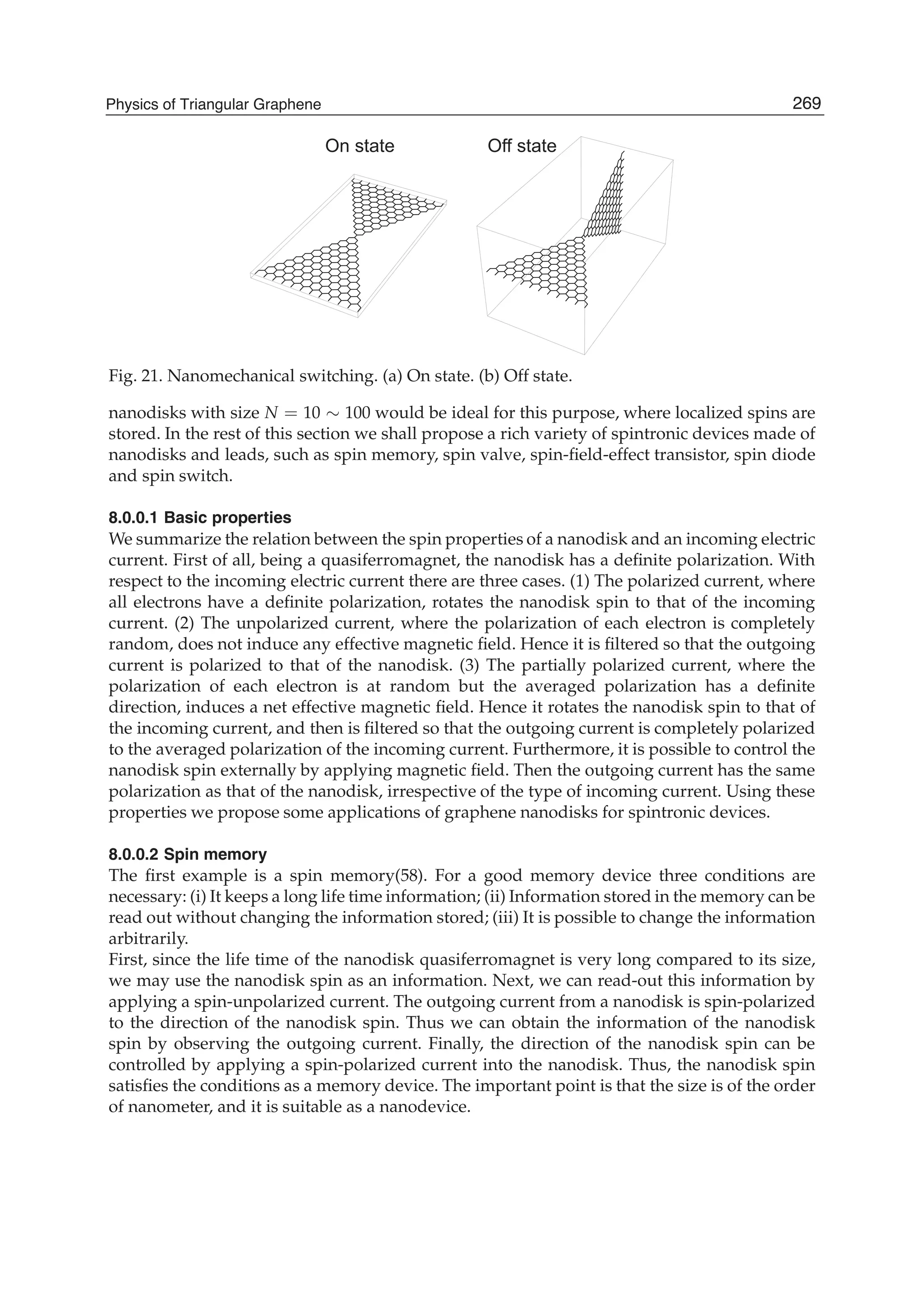
![(a)
(b)
spin filter
L
M
R
M
Fig. 22. (a) An electron tunnels from the left lead to the nanodisk and then to the right lead.
Only electrons with the same spin direction as the nanodisk spin can pass through the
nanodisk freely. As a result, when we apply a spin-unpolarized current to the nanodisk, the
outgoing current is spin polarized to the direction of the nanodisk spin. Consequently, this
system acts as a spin filter. (b) The system is a reminiscence of a metal-ferromagnet-metal
junction.
8.0.0.3 Spin filter
We make an investigation of the spin-filter effects(64). We first analyze how spin of a nanodisk
filters spin of the current by assuming that the nanodisk is a rigid ferromagnet. However, since
the nanodisk is not a rigid ferromagnet but a quasiferromagnet, its spin can be controlled by
the spin of the current. We analyze the reaction to the spin of the nanodisk from the spin of
electrons in the current.
We go on to investigate applications of nanodisks to spintronics. The basic one is a spin
filter(75). We consider a lead-nanodisk-lead system, where an electron makes a tunnelling
from the left lead to the nanodisk and then to the right lead. This system is a reminiscence of a
metal-ferromagnet-metal junction (Fig.22). If electrons in the lead has the same spin direction
as the nanodisk spin, they can pass through the nanodisk freely. However, those with the
opposite direction feel a large Coulomb barrier and are blocked (Pauli blockade)(64). As a
result, when we apply a spin-unpolarized current to the nanodisk, the outgoing current is
spin polarized to the direction of the nanodisk spin. Consequently, this system acts as a spin
filter.
8.0.0.4 Spin valve
A nanodisk can be used as a spin valve, inducing the giant magnetoresistance effect(76–78).
We set up a system composed of two nanodisks sequentially connected with leads [Fig.23].
We apply external magnetic field, and control the spin direction of the first nanodisk to be
|θ = cos θ
2 |↑ + sin θ
2 |↓ , and that of the second nanodisk to be |0 = |↑ . We inject an
unpolarized-spin current to the first nanodisk. The spin of the lead between the two nanodisks
is polarized into the direction of |θ . Subsequently the current is filtered to the up-spin one by
the second nanodisk. The outgoing current from the second nanodisk is
Iout
↑ = I cos
θ
2
. (74)
We can control the magnitude of the up-polarized current from 0 to I by rotating the external
magnetic field. The system act as a spin valve.
8.0.0.5 Spin switch
We consider a chain of nanodisks and leads connected sequentially (Fig.22). Without external
magnetic field, nanodisk spins are oriented randomly due to thermal fluctuations, and a
270 Physics and Applications of Graphene - Theory](https://image.slidesharecdn.com/grrphysicsandapplicationsofgraphene-theory-140422181144-phpapp02/75/physics-and_applications_of_graphene_-_theory-280-2048.jpg)
![(a)
(b)
(c)
spin valve
RL
M M M
RL
Fig. 23. Illustration of spin valve. (a) The spin valve is made of two nanodisks with the same
size, which are connected with leads. (b) The system is analogous to the one made of metals
and ferromagnets. (c) Applying external magnetic field, we control the spin direction of the
first nanodisk to be |θ , and that of the second nanodisk to be |0 = |↑ . The incomming
current is unpolarized, but the outgoing current is polarized, Iout
↑ = I cos θ
2 , Iout
↓ = 0. Its
magnitude can be controlled continuously. This acts as a spin valve.
M M M
M M M M M
M M
RL
without magnetic field
spin switch
with magnetic field
Fig. 24. A chain of nonodisks and leads acts as a spin switch. Without external magnetic field,
nanodisk spins are oriented randomly due to thermal fluctuations, and a current cannot go
through the chain. However, as soon as a uniform magnetic field is applied to all nanodisks,
the direction of all nanodisk spins become identical and a current can go through.
current cannot go through the chain. However, when and only when a uniform magnetic field
is applied to all nanodisks, the direction of all nanodisk spins become identical and a current
can go through. Thus the system acts as a spin switch, showing a giant magnetoresistance
effect. The advantage of this system is that a detailed control of magnetic field is not necessary
in each nanodisk.
8.0.0.6 Spin-field-effect transistor
We again set up a system composed of two nanodisks sequentially connected with leads
[Fig.25]. We now apply the same external magnetic field to both these nanodisks, and fix
their spin direction to be up, |0 = |↑ . As an additional setting, we use a lead acting as a
spin rotator with the spin-rotation angle θ. The outgoing current from the second nanodisk
is Iout
↑ = I cos θ
2 . It is possible to tune the angle θ by applying an electric field. Hence we
can control the magnitude of the up-polarized current. The system acts as a spin-field-effect
transistor(79).
271Physics of Triangular Graphene](https://image.slidesharecdn.com/grrphysicsandapplicationsofgraphene-theory-140422181144-phpapp02/75/physics-and_applications_of_graphene_-_theory-281-2048.jpg)
![(a)
(b)
spin-field-effect transisitor
RL
RL
spin rotator
(a)
(b)
spin diode
RL
RL
spin rotator
(c)
RL
Fig. 25. (Left) Illustration of spin-field-effect transistor made of two nanodisks with the same
size. Two nanodisks are connected with a rotator. We set the spin direction of the two
nanodisks to be up by magnetic field. The incomming current is unpolarized, but the
outgoing current is polarized and given by Iout
↑ = I cos θ
2 , Iout
↓ = 0. The up-spin current is
rotated by the angle θ within the central lead ascting as a rotator. Illustration of spin diode
made of two nanodisks with different size. By controlling the bias voltage Δμ, the current
flows from the left lead to the right lead (Δμ > 0), or in the opposite way (Δμ < 0). The
incoming current is unpolarized, which is made polarized by the first nanodisk. The electron
spin in the central lead is rotated by the Rashba-type interaction. (Right) Illustration of spin
diode made of two nanodisks with different size. By controlling the bias voltage Δμ, the
current flows from the left lead to the right lead (Δμ > 0), or in the opposite way (Δμ < 0).
The incoming current is unpolarized, which is made polarized by the first nanodisk. The
electron spin in the central lead is rotated by the Rashba-type interaction.
8.0.0.7 Spin diode
The third example is a spin diode [Fig.25]. We set up a system composed of two nanodisks
sequentially connected with leads, where two nanodisks have different sizes. The left
nanodisk is assumed to be larger than the right nanodisk. Then the relaxation time of the left
nanodisk τL(≡ τL
filter) is larger than that of the right nanodisk τR(≡ τR
filter), τL > τR. Second,
the applied magnetic field is assumed to be so small that the nanodisk spin can be controlled
by a polarized current. For definiteness we take the direction of the magnetic field to be up.
Third, the lead is assumed to have the Rashba-type interaction(80),
HR =
λ
¯h
pxσy
− pyσx
. (75)
Spins make precession while they pass through the lead. The spin-rotation angle is given(55)
by
Δθ =
2λm∗L
¯h
, (76)
where m∗ is the electron effective mass in the lead and L is the length of the lead. We can
control Δθ by changing the coupling strength λ externally by applying electric field(81).
When no currents enter the nanodisk, the direction of two nanodisk spins is identical due to
the tiny external magnetic field, which is up. When we inject the current in this state, the net
outgoing current is very small,
Iout
= cos Δθ 0 for Δθ ≈ π. (77)
272 Physics and Applications of Graphene - Theory](https://image.slidesharecdn.com/grrphysicsandapplicationsofgraphene-theory-140422181144-phpapp02/75/physics-and_applications_of_graphene_-_theory-282-2048.jpg)
![11. References
[1] M. S. Dresselhaus, G. Dresselhaus, K. Sugihara, I. L. Spain and H. A. Goldberg, Graphite
Fibers and Filaments, Springer Series in Material Science Vol 5 (Springer-Verlag, Berlin,
1988).
[2] J. W. McClure, Phys.Rev. 104, 666 (1956).
[3] S. Iijima, Nature (London) 354, 56 (1991).
[4] N. Hamada, S. I. Sawada, and A. Oshiyama, Phys. Rev. Lett. 68, 1579 (1992).
[5] R. Saito, M. Fujita, G. Dresselhaus, and M. S. Dresselhaus, Appl. Phys. Lett. 60, 18 (1992).
[6] J. W. Mintmire, B. I. Dunlap, and C. T. White, Phys. Rev. Lett. 68, 631 (1992).
[7] R. Saito, G. Dresselhaus, and M. S. Dresselhaus, Physical Properties of Carbon Nanotubes,
Imperial College Press, 1998, London.
[8] J. W. G. Wildöer, L. C. Venema, A. G. Rinzler, R. E. Smalley, and C. Dekker, Nature
(London) 391, 59 (1998).
[9] A. Jorio, R. Saito, J. H. Hafner, C. M. Lieber, M. Hunter, T. McClure, G. Dresselhaus, and
M. S. Dresselhaus, Phys. Rev. Lett. 86, 1118 (2001).
[10] M. Ouyang, J. L. Huang, C. M. Lieber, Ann. Rev. Phys. Chem 53, 201 (2002).
[11] H. W. Kroto, J. R. Heath, S. C. O’Brien, R. F. Curl, R. E. Smalley, Nature (London) 318, 167
(1985).
[12] K.S. Novoselov, A. K. Geim, S. V. Morozov, D. Jiang, Y. Zhang, S. V. Dubonos, I. V.
Grigorieva, and A. A. Firsov, Science 306, 666 (2004).
[13] K.S. Novoselov, A. K. Geim1, S. V. Morozov, D. Jiang1, M. I. Katsnelson, I. V. Grigorieva,
S. V. Dubonos and A. A. Firsov, Nature 438, 197 (2005).
[14] Y. Zhang, Yan-Wen Tan, Horst L. Stormer and Philip Kim, Nature 438, 201 (2005).
[15] A. H. Castro Neto, F. Guinea, N. M. R. Peres, K. S. Novoselov and A. K. Geim, Rev. Mod.
Phys. 81, 109 (2009).
[16] D. J. Klein, Chem. Phys. Lett. 217, 261 (1994).
[17] M. Fujita, K. Wakabayashi, K. Nakada, and K. Kusakabe, J. Phys. Soc. Jpn. 65, 1920 (1996).
[18] Y. Niimi, T. Matsui, H. Kambara, K. Tagami, M. Tsukada, and H. Fukuyama. Appl. Surf.
Sci. 241, 43 (2005). Y. Kobayashi, K. Fukui, T. Enoki and K. Kusakabe, Phys. Rev. B, 73,
125415 (2006).
[19] O. E. Andersson, B. L. V. Prasad, H. Sato, T. Enoki, Y. Hishiyama, Y. Kaburagi, M.
Yoshikawa and S. Bandow, Phys. Rev. B, 58, 16387 (1998).
[20] K. Kusakabe and M. Maruyama, Phys. Rev. B, 67, 092406 (2003).
[21] M. Ezawa, Physical Review B, 73, 045432 (2006).
[22] L. Brey, and H. A. Fertig, Phys. Rev. B, 73, 235411 (2006).
[23] F. Muñoz-Rojas, D. Jacob, J. Fernández-Rossier, and J. J. Palacios, Phys. Rev. B, 74, 195417
(2006).
[24] Y. -W Son, M. L. Cohen, and S. G. Louie, Phys. Rev. Lett., 97, 216803 (2006).
[25] V. Barone, O. Hod, and G. E. Scuseria, Nano Lett., 6, 2748 (2006).
[26] M. Y. Han, B. Oezyilmaz, Y. Zhang, and P. Kim, Phys. Rev. Lett., 98, 206805 (2007).
[27] Z. Chen, Y. -M. Lin, M. J. Rooks, and P. Avouris, Physica E, 40, 228 (2007).
[28] Z. Xu and Q. -S. Zheng, Appl. Phys. Lett. 90, 223115 (2007).
274 Physics and Applications of Graphene - Theory](https://image.slidesharecdn.com/grrphysicsandapplicationsofgraphene-theory-140422181144-phpapp02/75/physics-and_applications_of_graphene_-_theory-284-2048.jpg)
![[29] B. Özyilmaz, P. Jarillo-Herrero, D. Efetov and P. Kim, Appl. Phys. Lett. 91, 192107 (2007).
[30] Y.W. Son, M.L. Cohen and S.G. LouieSon, Nature 444, 347 (2006).
[31] O.Hod, V. Barone, J.E. Peralta and G.E. Scuseria, Nano Lett. 7, 2295 (2007).
[32] See http://sciencewatch.com/ana/st/graphene/.
[33] C. Berger, Z. Song, X. Li, X. Wu, N. Brown, C. Naud, D. Mayou, T. Li, J. Hass, A.N.
Marchenkov, E. H. Conrad, P.N. First and W. A. de Heer, Science 312, 119 (2006).
[34] H. J. Räder, A. Rouhanipour, A. M. Talarico, V. Palermo, P. Samorì, and K. Müllen, Nature
materials 5, 276 (2006).
[35] M. Ezawa, Physica Status Solidi (c) 4, No.2, 489 (2007).
[36] M. Ezawa, Phys. Rev. B 76, 245415 (2007): M. Ezawa, Physica E 40, 1421-1423 (2008).
[37] J. Fernández-Rossier, and J. J. Palacios, Phys. Rev. Lett. 99, 177204 (2007).
[38] W. L. Wang, S. Meng, and E. Kaxiras, Nano Lett 8, 241 (2008).
[39] W. L. Wang, Oleg V. Yazyev, S. Meng, and E. Kaxiras, Phys. Rev. Lett. 102, 157201 (2009).
[40] J. Akola, H. P. Heiskanen, and M. Manninen, Phys. Rev. B 77, 193410 (2008).
[41] O. V. Yazyev, Rep. Prog. Phys 73, 5 (2010).
[42] A. D. Güçlü, P. Potasz, O. Voznyy, M. Korkusinski, and P. Hawrylak, Phys. Rev. Lett. 103,
246805 (2009).
[43] P. Potasz, A. D. Güçlü and P. Hawrylak, Phys. Rev. B 81, 033403 (2010).
[44] L. C. Campos, V. R. Manfrinato, J. D. Sanchez-Yamagishi, J. Kong and P. Jarillo-Herrero,
Nano Lett., 9, 2600 (2009).
[45] O. Hod, V. Barone, and G. E. Scuseria, Phys. Rev. B 77, 035411 (2008).
[46] M. Ezawa, Phys. Rev. B 77, 155411 (2008).
[47] M. Ezawa, Phys. Rev. B 79, 241407(R) (2009).
[48] M. Ezawa, Phys. Rev. B 81, 201402(R) (2010).
[49] J.C. Slonczewski and P.R. Weiss, Phys. Rev. 109, 272 (1958).
[50] G. W. Semenoff, Phys. Rev. Lett. 53, 2449 (1984).
[51] H. Ajiki and T. Ando, J. Phys. Soc. Jpn., 62, 1255 (1993); T. Ando, Y. Zheng and H. Suzuura,
Microelectronic Engineering, 63, 167 (2002).
[52] S. Murakami, N. Nagaosa, S.-C. Zhang, Science 301, 1348 (2003).
[53] Y. Ohno, D. K. Young, B. Beschoten, F. Matsukura, H. Ohno and D. D. Awschalom, Nature
402, 790 (1999).
[54] See, e.g., Realizing Controllable Quantum States: Mesoscopic Superconductivity and
Spintronics, edited by H. Takayanagi and J. Nitta, World Scientific, Singapore, 2005,
and references therein.
[55] I. Zˇuti´c, J. Fabian and S. Das Sarma, Rev. Mod. Phys., 76, (2004), and references therin.
[56] S. A. Wolf, D. D. Awschalom, R. A. Buhrman, J. M. Daughton, S. von Molnár, M.L.Roukes,
A. Y. Chtchelkanova and D. M. Treger, Science 294, 1488 (2001), and references therin.
[57] G. A. Prinz, Science 282, 1660 (1998), and references therin.
[58] P. Recher, E. V. Sukhorukov and D. Loss, Phys. Rev. Lett., 85, 1962 (2000).
[59] J. A. Folk, R. M. Potok, C. M. Marcus and V. Umansky, Science 299, 679 (2003).
[60] N. Tombros, C. Jozsa, M. Popinciuc, H. T. Jonkman, B. J. van Wees, Nature 448, 571 (2007).
275Physics of Triangular Graphene](https://image.slidesharecdn.com/grrphysicsandapplicationsofgraphene-theory-140422181144-phpapp02/75/physics-and_applications_of_graphene_-_theory-285-2048.jpg)
![[61] V. M. Karpan, G. Giovannetti, P. A. Khomyakov, M. Talanana, A. A. Starikov, M.
Zwierzycki, J. van den Brink, G. Brocks, P. J. Kelly, Phys Rev Lett 99, 176602 (2007).
[62] L.Brey, H.A.Fertig, Phys. Rev. B 76, 205435 (2007).
[63] M. Wimmer, N. Adagideli, S. Berber, D. Tománek, and K. Richter, Phys. Rev. Lett., 100,
177207 (2008).
[64] M. Ezawa, Eur. Phys. J. B 67, 543 (2009).
[65] M. Ezawa, New J. Phys., 11, 095005 (2009).
[66] M. Ezawa, Physica E 42, 703-706 (2010).
[67] K.S. Novoselov, E. McCann, S. V. Morozov, V. I. Fal’ko, M. I. Katsnelson, U. Zeitler, D.
Jiang, F. Schendini and A. K. Geim, Nature Phys. 2, 177 (2006).
[68] S. Fajtlowicz, P. E. John, and H. Sachs, Croat. Chem. Acta 78, 195. (2005).
[69] S.Y. Zhou, G.-H. Gweon, J. Graf, A. V. Fedorov, C. D. Spataru, R. D. Diehl, Y. Kopelevich,
D.-H. Lee, S.G. Louie, A. Lanzara, Nature Phys. 2, 595 (2006).
[70] T. Matsuda, S. Hasegawa, M. Igarashi, T. Kobayashi, M. Naito, H. Kajiyama, J. Endo, N.
Osakabe and A. Tonomura, Phys. Rev. Lett. 62, 2519 (1989).
[71] M. Kinza, J. Ortlo, and C. Honerkamp, cond-mat/arXiv:1002.2513
[72] E. H. Lieb, Phys. Rev. Lett. 62, 1201 (1989).
[73] L. Pisani, J.A. Chan, B. Montanari and N.M. Harrison, Phys. Rev. B 75, 64418 (2007).
[74] J. P. Hobson and W. A. Nierenberg, Phys. Rev. 89, 662 (1953).
[75] T. Koga, J. Nitta, H. Takayanagi and S. Datta, Phys. Rev. Lett. 88, 126601 (2002).
[76] M. N. Baibich, J. M. Brot, A. Fert, N. V. Dau and F. Petroff, Phys. Rev. Lett. 61, 2472 (1988).
[77] G. Binasch, P. Grunberg, F. Saurenbach and W. Zinn, Phys. Rev. B 39, 4828 (1989).
[78] Y. M. Lee, J. Hayakawa, S. Ikeda, F. Matsukura and H. Ohno, Appl. Phys. Lett. 90, 212507
(2007).
[79] S. Datta and B. Das, Appl. Phys. Lett. 56, 665 (1990).
[80] E. I. Rashba, Fiz. Tverd. Tela (Leningrad) 2, 1224 (1960) [Sov. Phys. Solid State 2, 1109
(1960)]; Y. A. Bychkov and E. I. Rashba, J. Phys. C 17, 6039 (1984).
[81] J. Nitta, T. Akazaki, and H. Takayanagi, Phys. Rev. Lett. 78, 1335 (1997).
276 Physics and Applications of Graphene - Theory](https://image.slidesharecdn.com/grrphysicsandapplicationsofgraphene-theory-140422181144-phpapp02/75/physics-and_applications_of_graphene_-_theory-286-2048.jpg)
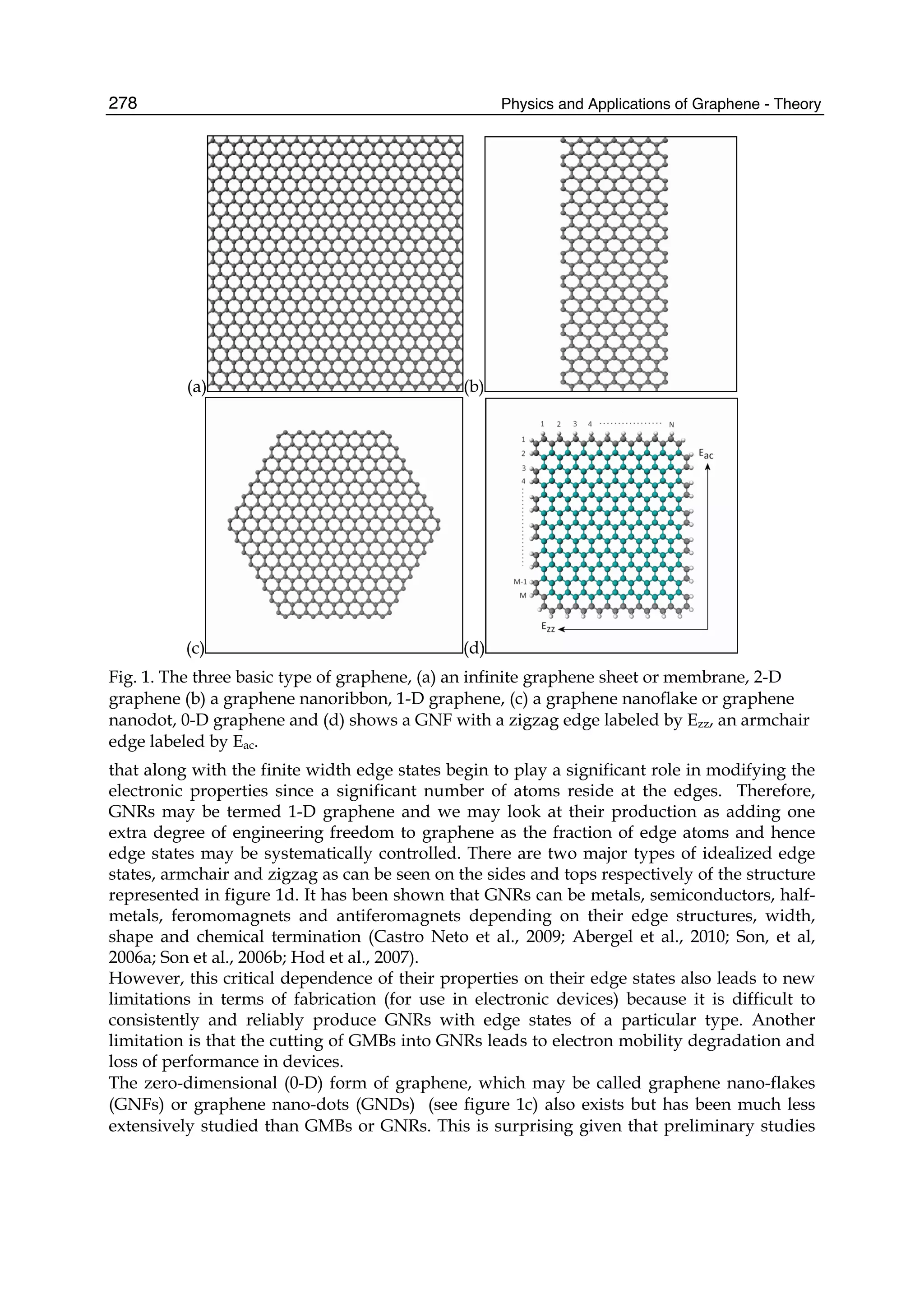
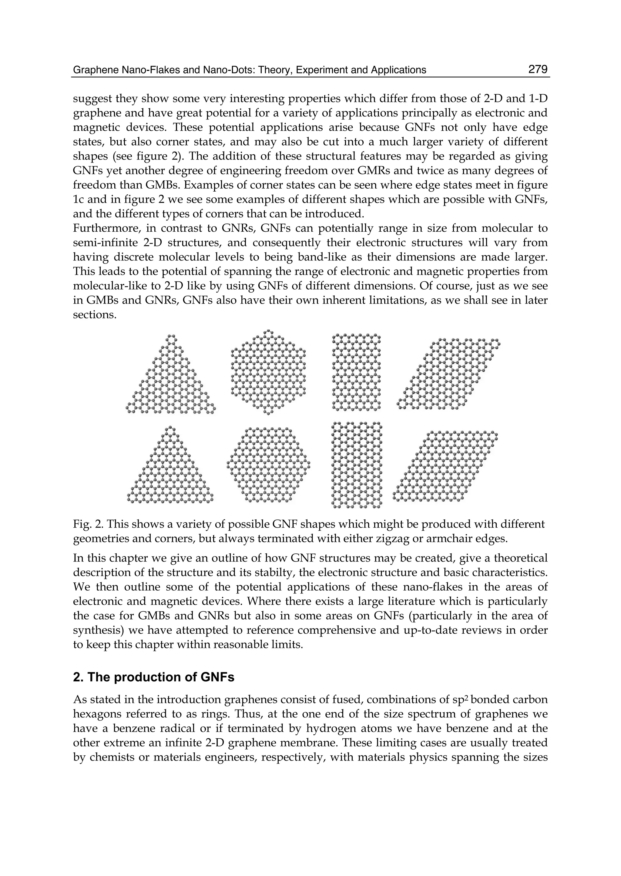
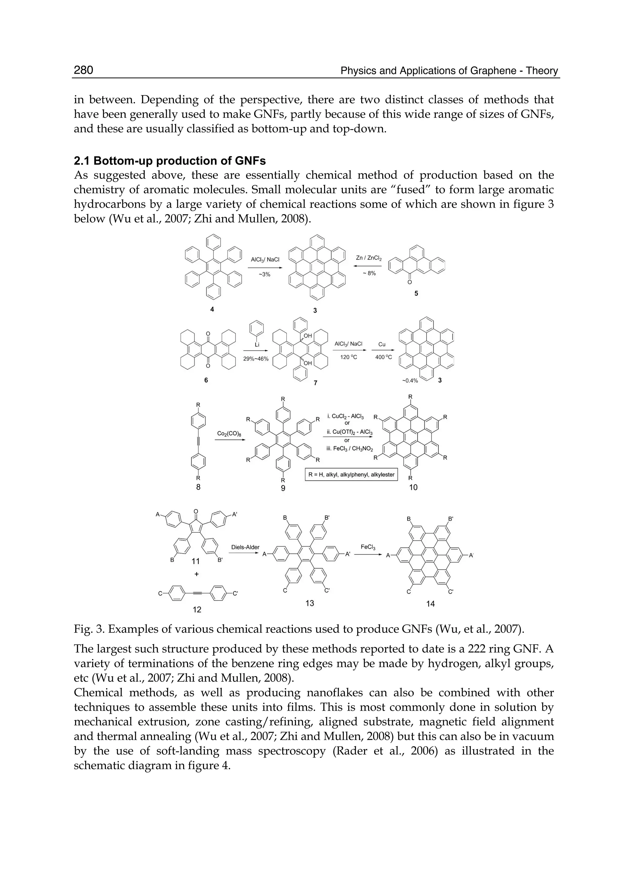
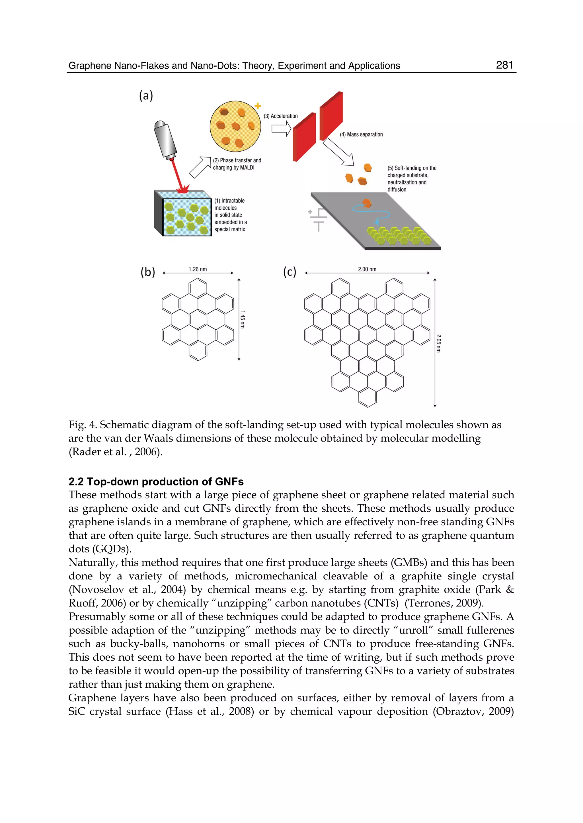
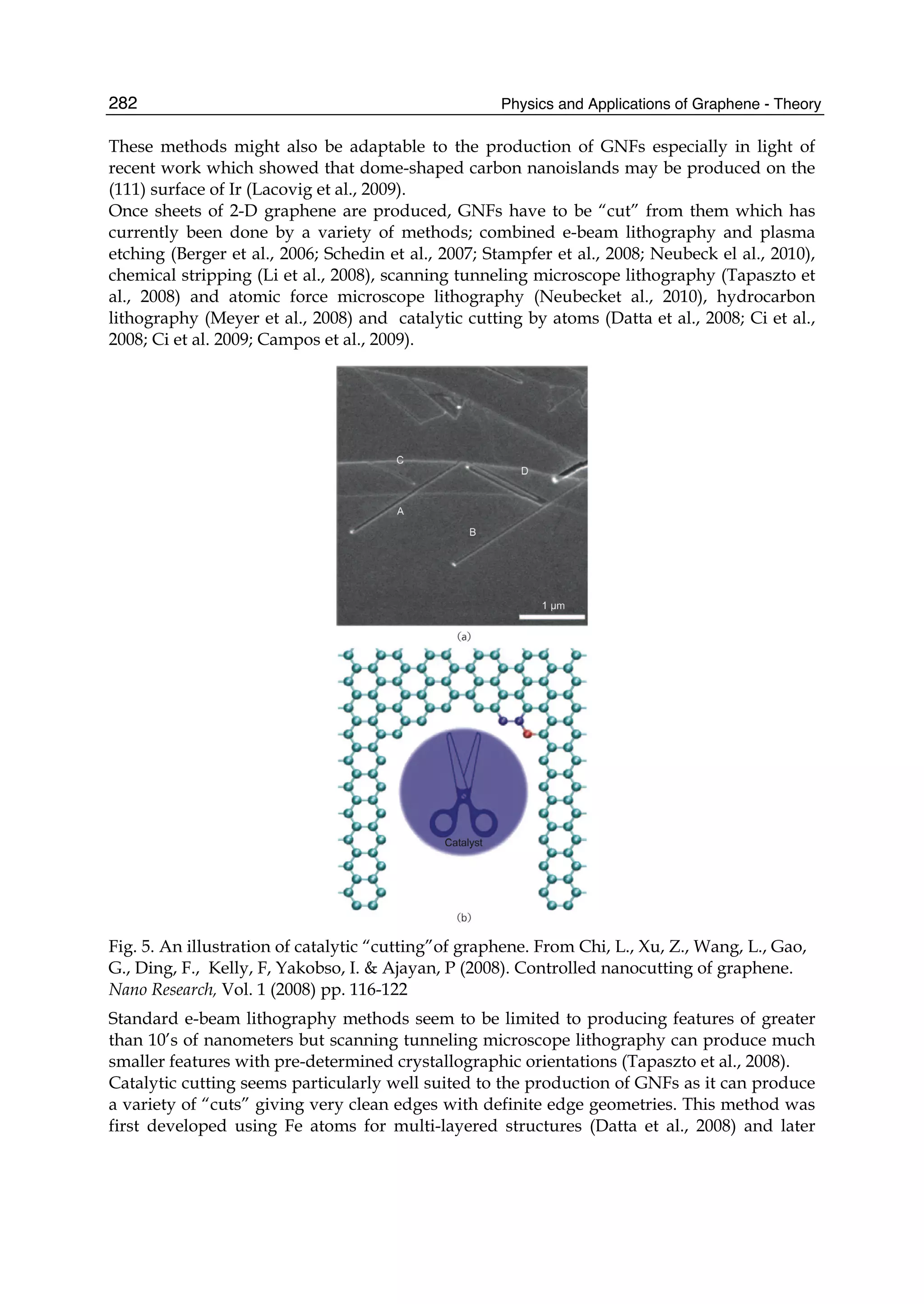
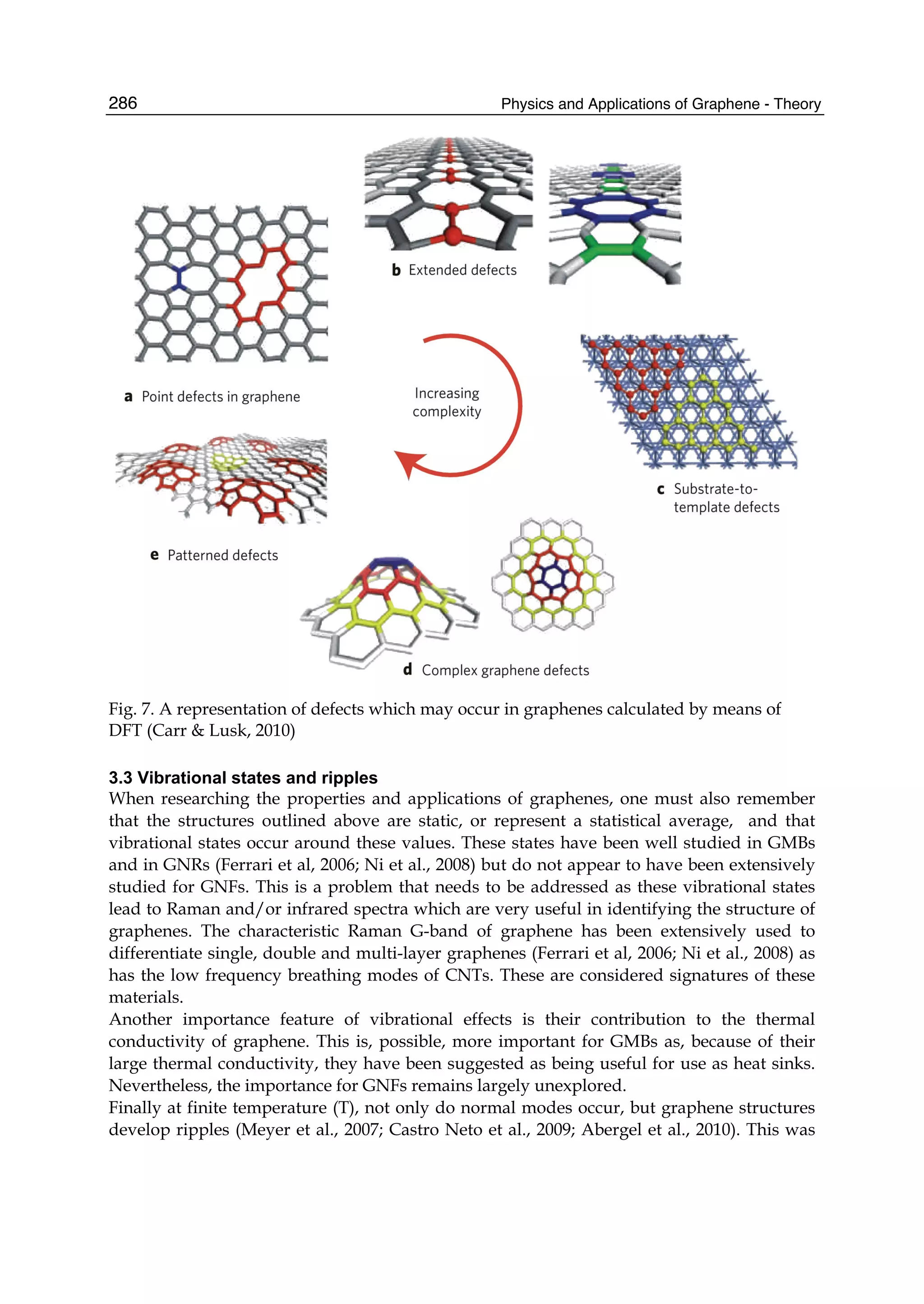
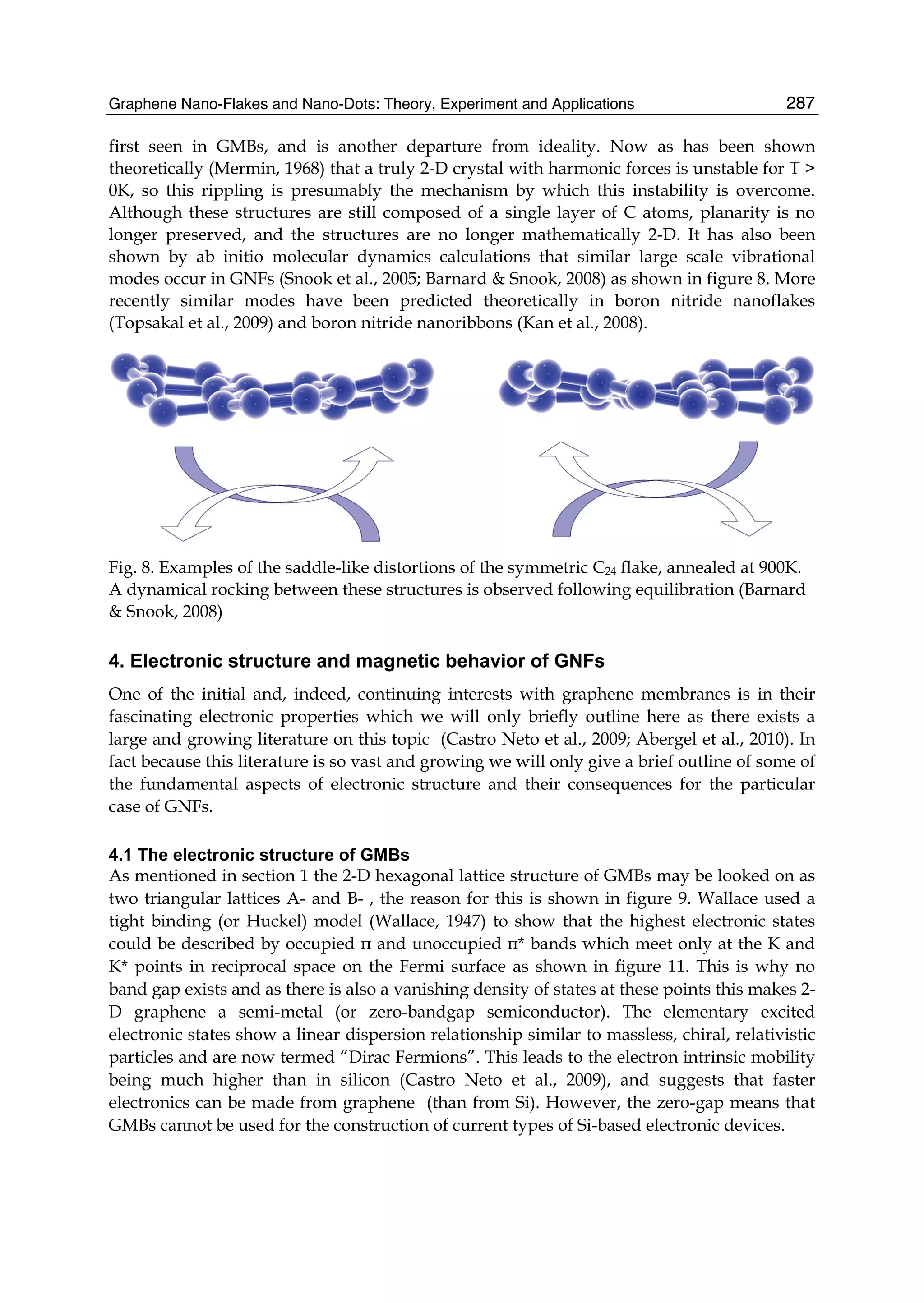
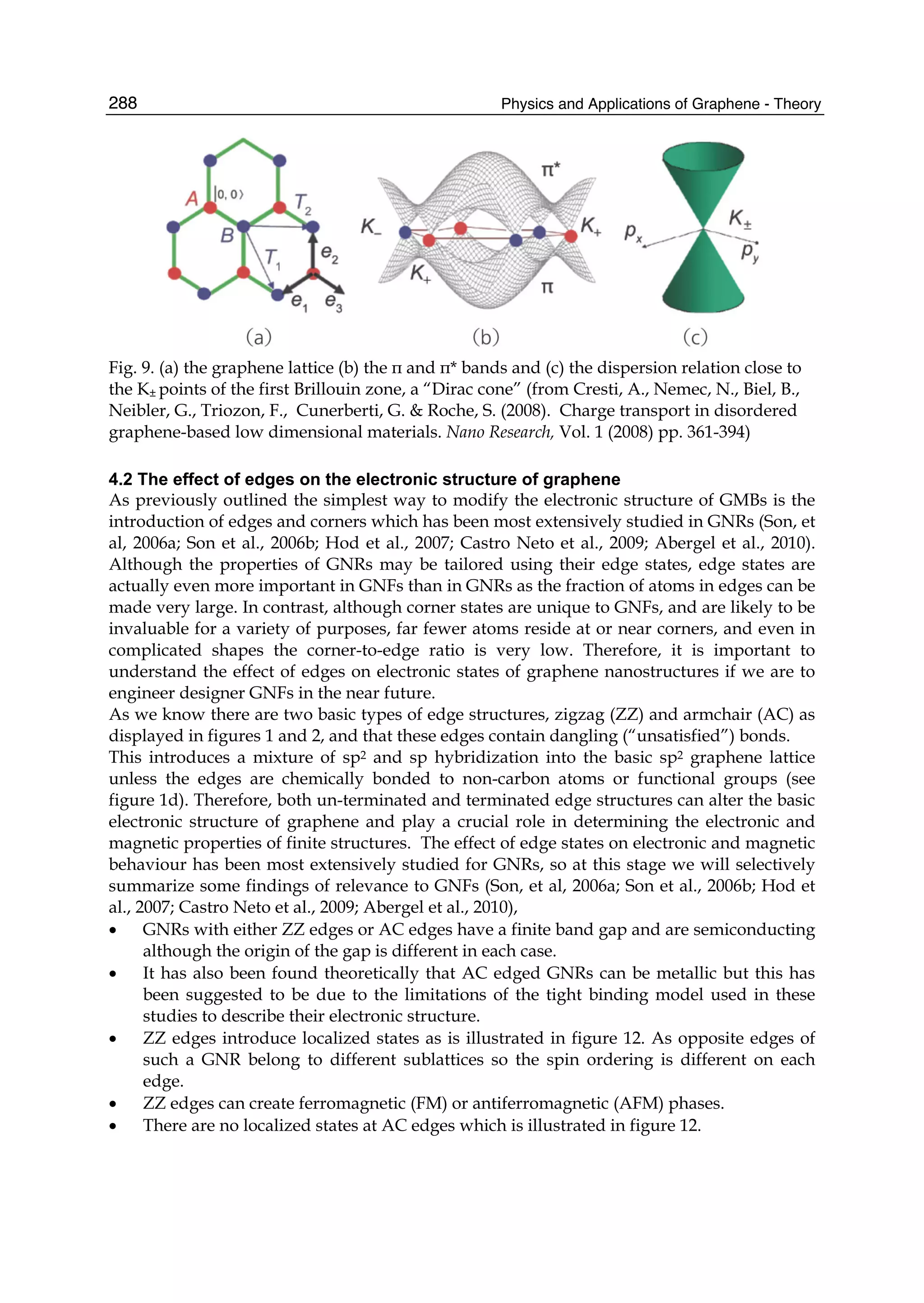
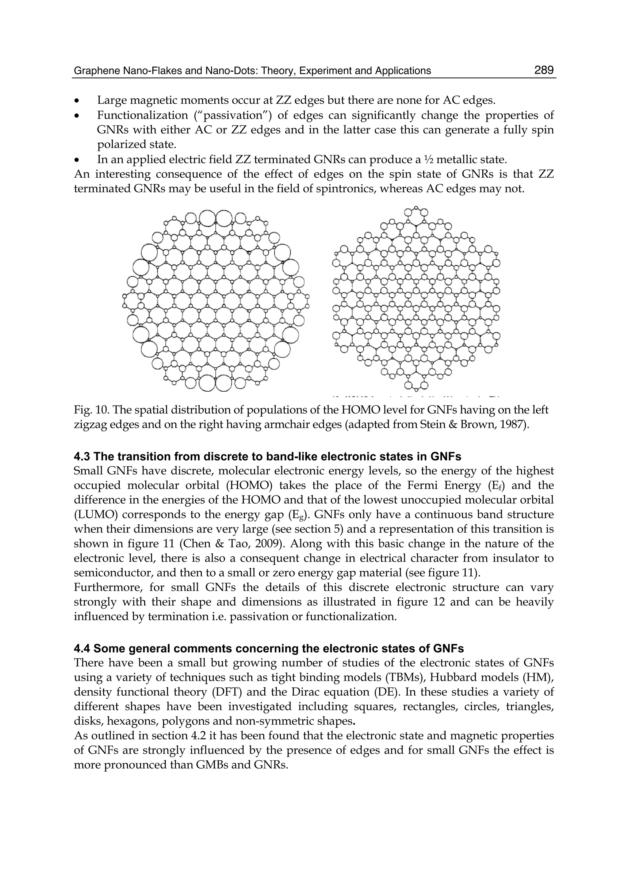
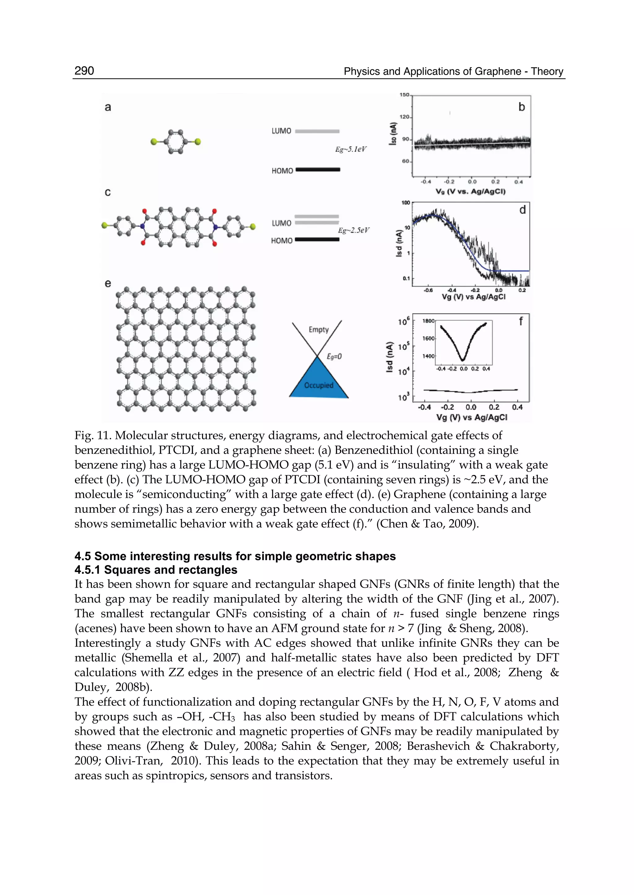
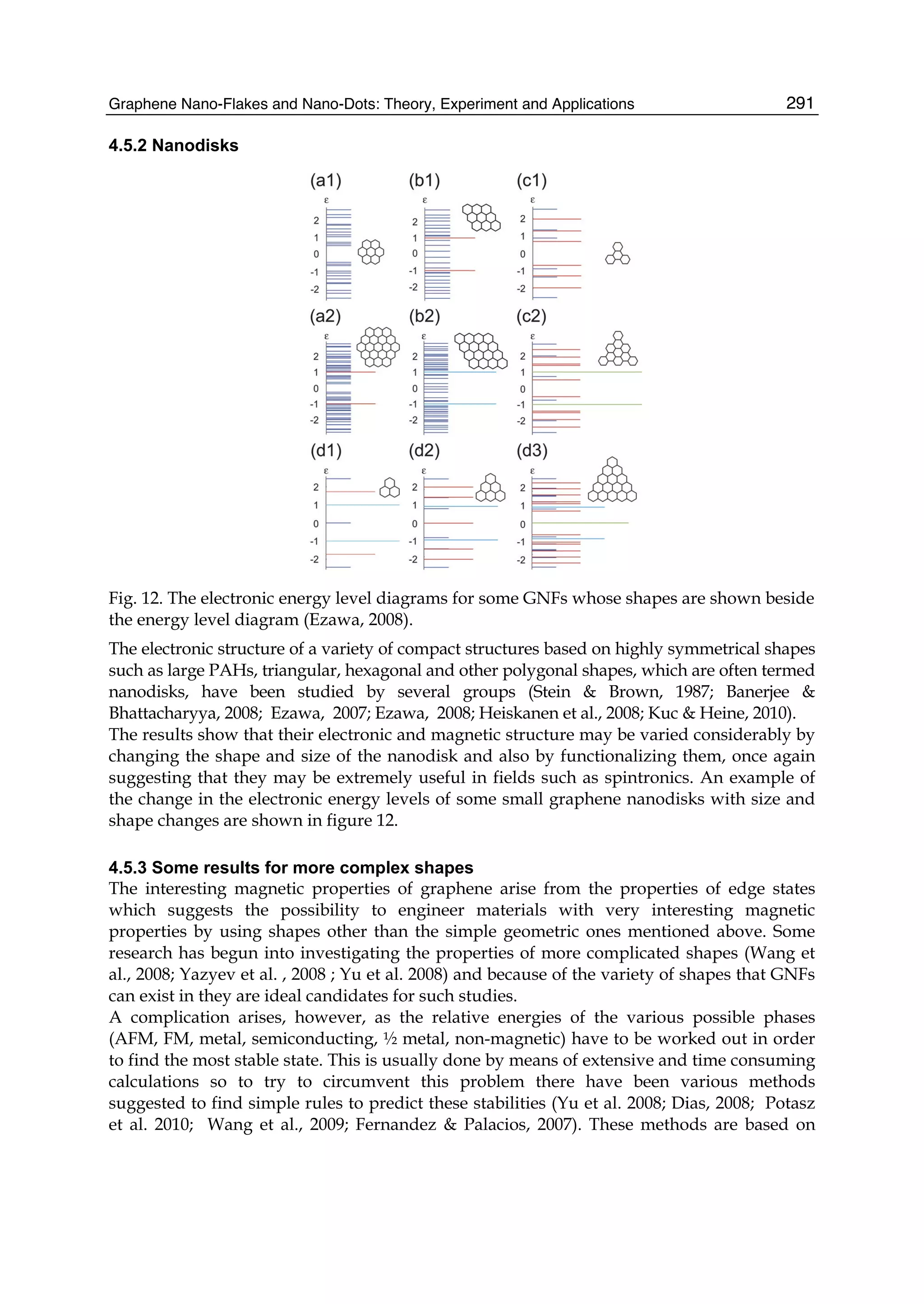
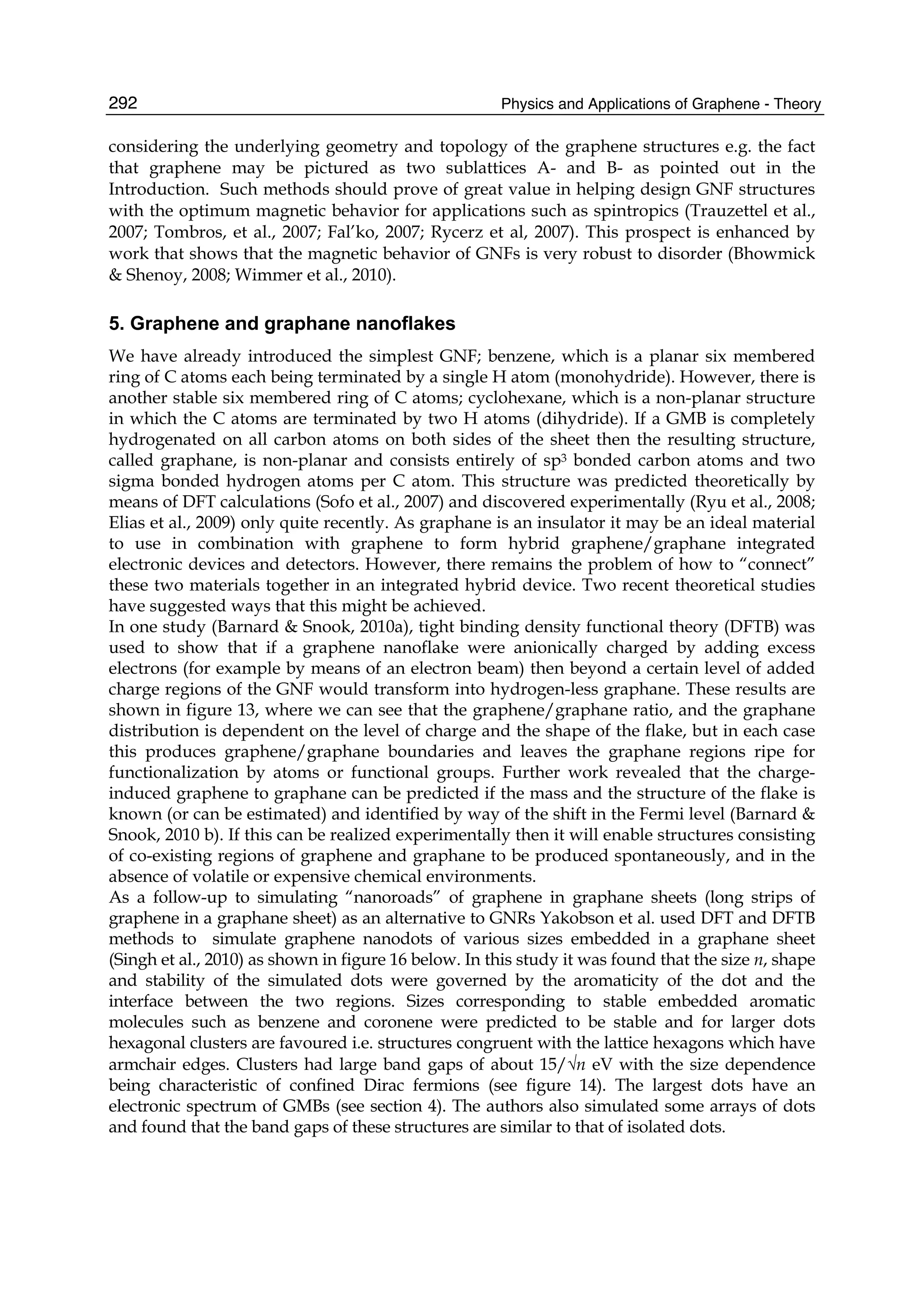
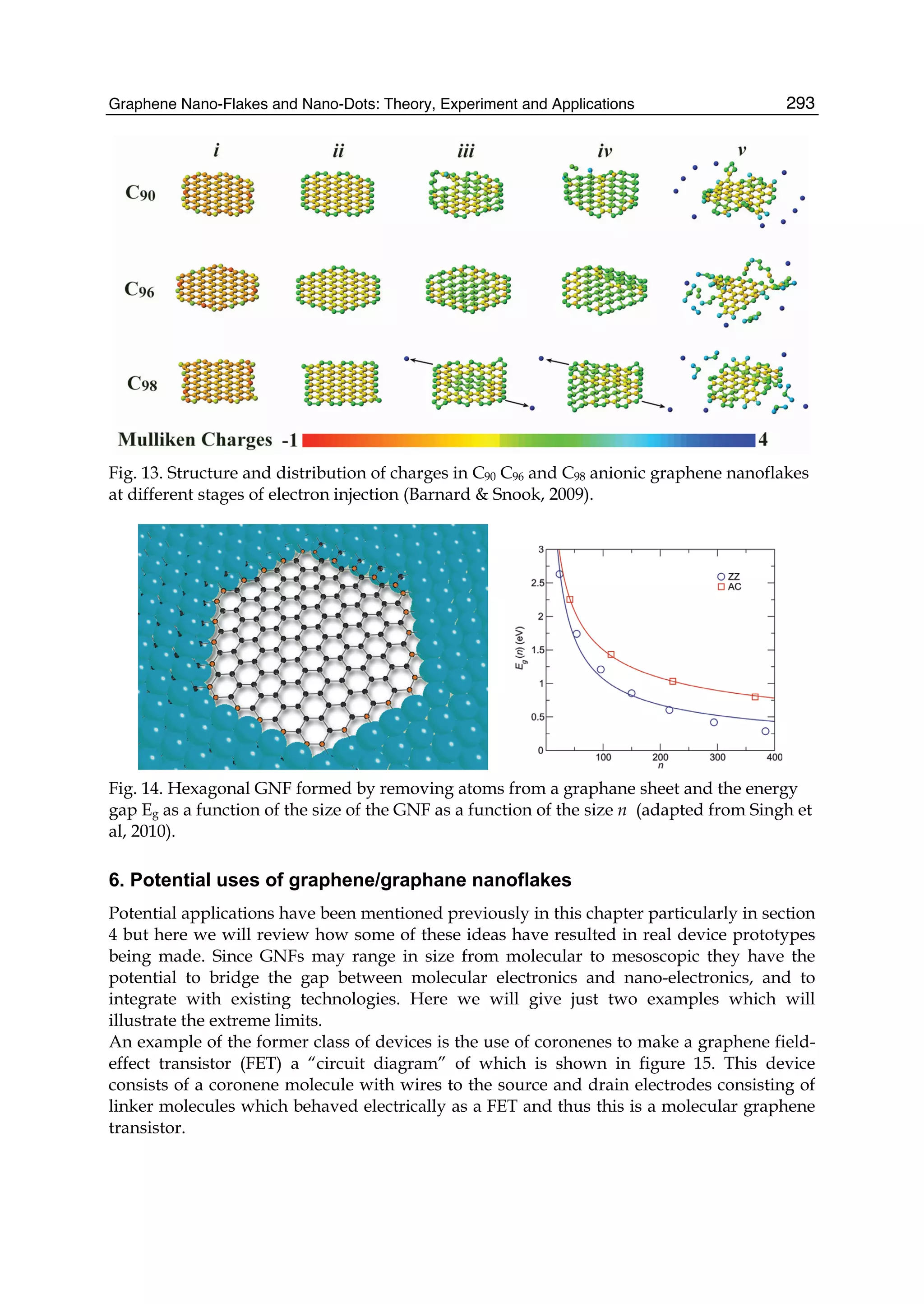
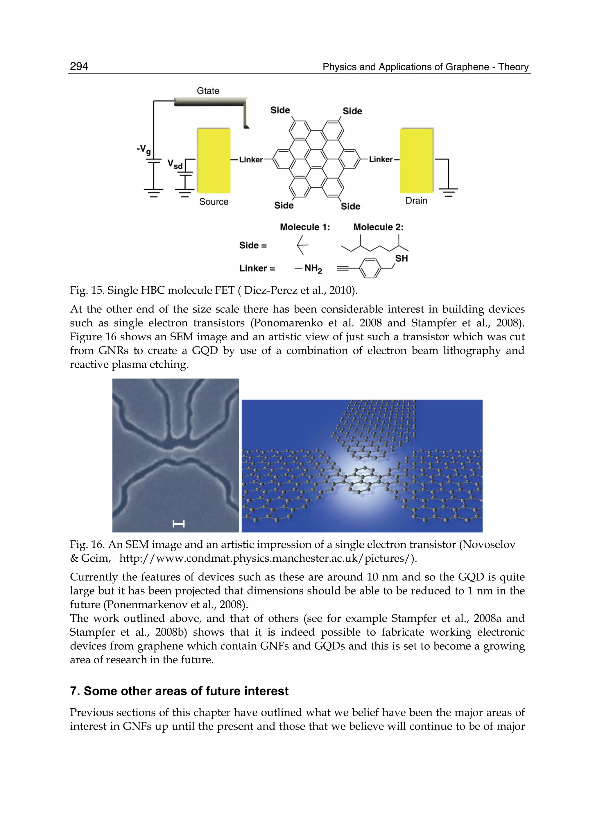
![1. Introduction
Since its characterization in 2004 [Novoselov et al. (2004; 2005)] graphene has emerged as a
material showing somehow rather unusual and particular characteristics [Castro Neto et al
(2009); Geim (2009); Katselnson et al. (2006)]. In October 2010 A. Geim and K. Novoselov
have been awarded the Physics Nobel Prize for the characterization of graphene. Much of
this particular behavior is due to its nature of a pure two dimensional (2-D) materials made
up of Carbon atoms in a honeycomb lattice. Moreover graphene, can be thought not only
as the constituting material of the well known graphite (made up of a series of graphene
stacks kept together by weak van der Waals bonds), but also as the constituent of other
carbon-based nanomaterial. For instance the well known carbon nanotubes [Charlier et al.
(2007)] can be considered as a rolled-up graphene sheet where edges have been joined.
Fullerene [Andreoni (2000)] on the other hand can be seen as graphene with the presence of
pentagonal defects responsible for the positive curvature that leads to the spherical geometry.
Despite its importance, and despite the fact that graphene sheets could be produced every
time someone uses a graphite-pencil, graphene was isolated and characterized only very
recently, due to the technically difficulties in evidencing its formation. Moreover, even if
theoretical considerations on the electronic structures of a single graphite sheets date back
to the work of Pauling in 1950s [Pauling (1972)], the existence of a purely 2-D systems
was considered as impossible until recently. However, soon afterwards its characterization
graphene has open the way to an impressive mole of experimental and theoretical studies
(see for instance Castro Neto et al (2009) and reference therein), in particular because of
its remarkable electronic properties that make graphene a very important material to be
exploited in the field of molecular and nano-electronics. Technical applications of graphene, or
graphene-based devices, can go from single molecule detection [Schedin et al. (2007)], to field
effect transistors [Novoselov et al. (2004)] and quantum information processing [Trauzettel et
al. (2007)]. One should also cite that the robustness of the σ skeleton of graphene makes it one
of the strongest materials ever tested [Lee et al. (2008)], and this fact obviously suggest the
possible use of carbon-fiber reinforcements in novel composite materials. Although our work
will not focus mainly on the properties of infinite graphene sheets, let us cite that graphene
also proved to be a zero gap semi-metal, characterized by a very high electron mobility.
Moreover, graphene is able to show unusual linearly dispersing electronic excitations: the
electronic excitations in the vicinity of the Fermi level remind those of massless Dirac
fermions. Graphene, therefore, allowed predictions of quantum electrodynamics to be tested
in a solid-state system. It is also noteworthy to cite that many of these findings have been
Antonio Monari1,2 and Stefano Evangelisti1
1Laboratoire de Chimie et Physique Quantiques. Université de Toulouse et CNRS.
2 Equipe de Chimie et Biochimie Théoriques, SRSMC, CNRS, Nancy-Université
France
Finite-Size Effects in Graphene Nanostructures
14](https://image.slidesharecdn.com/grrphysicsandapplicationsofgraphene-theory-140422181144-phpapp02/75/physics-and_applications_of_graphene_-_theory-313-2048.jpg)
![anticipated in the framework of independent electrons band theory by Wallace back in 1947
[Wallace (1947)]. Since then, even if theoretical works have become much more accurate
and have benefit of the possibility to compare to experiments, the role of electron-electron
correlation in graphene has been still an object of intense debate [Castro Neto et al (2009)].
Another very interesting problems, strongly related to electronic properties and to the Dirac
fermions, concerns the influence and effects produced by disorder in the physics of electrons
in graphene as well as its transport properties. Some of the parameters developed in the
following of this Chapter, and in particular the localization tensor, could be of seminal
importance in elucidating these effects.
If, as we have briefly recalled, infinite graphene presents absolutely remarkable properties,
also finite-size systems (nano ribbons or nano islands) show a behavior that needs a careful
investigation [Berger et al. (2006)]. In particular the geometry of the islands, and especially
the form of edges, can module the properties of the system in a very impressive way
[Castro Neto et al (2009)]. We would like to stress that in the near past the control over the
nano-islands geometry was rather poor, due to the fact that graphene was produced by a
top-down approaches by stripping away sheets from graphite. Today, on the other hand,
with the emergence of bottom-up approaches, based on controlled deposition on metallic
surfaces (for instance Ruthenium), the control of the final system geometry has significantly
improved, and it is now possible to produce nano-islands of different size and forms with
atomically defined edges [Fernandéz-Rossier & Palacios (2007)], ranging from the quasi-one
dimensional ribbons to the zero-dimension dots. One of the first and better known and studied
finite-size effect on graphene is the emergence of edge-states in the case of nano-ribbons
[Son et al. (2004)]. From a physical points of view this means that the electrons close to
the Fermi level tend to preferentially occupy regions of space that are close to the borders
of the ribbon. This feature has been observed experimentally and has been predicted with
high level ab initio computations for instance by Hod et al. (2008; 2007). It is also known that
the behavior of the nano-ribbon strongly depends on the type of edges, giving rise to the
two well known classes of "zig-zag" and "armchair" edges. More complex structures, such as
hexagonal, rhomboidal and triangular ones, will show an even more complex behavior and
can also give rise to open shell, high multiplicity ground states [Fernandéz-Rossier & Palacios
(2007); Yu et al. (2008); Ezawa (2007)]. This could result in the possibility of rationally design
advanced nano-magnets, also exploiting the connection of different multiplicity sub-units (see
for instance the works of Yu et al. (2008); Trinquier et al. (2010)). In the same way, as suggest
by Fürst et al (2009) the possibility to create antidot graphene lattices, in which graphene
can be artificially periodically perforated to create a precise arrangement of holes, appears
very promising to further control and module electronic properties. All this attempts can be
seen as steps toward the production of metametarials [Pendry et al. (1996)], i.e. materials
that derive their properties from their artificial, man-made, periodic small-scale structure.
Anyway it is noteworthy to cite also all the attempts made to enhance physically properties
of graphene-like structures by their interaction with atoms or small molecules, for instance
following the procedure of the spin doping.
1.1 Magnetic properties of graphene nano-systems
An important feature to rationalize the relation between structure and electronic properties,
and more generally, to study finite size effects on graphene nano-structures, is to recognize
that the honeycomb graphene is composed by a bipartite lattice [Fernandéz-Rossier & Palacios
(2007)], with two compenetrating triangular sublattices A and B. Each atom constituting the
304 Physics and Applications of Graphene - Theory](https://image.slidesharecdn.com/grrphysicsandapplicationsofgraphene-theory-140422181144-phpapp02/75/physics-and_applications_of_graphene_-_theory-314-2048.jpg)
![graphene can be associated to one of the two sublattices, one can therefore speak of A and B
graphene atoms or centers. Moreover, each A atom will only have B nearest neighborings and
viceversa. So for instance, zig-zag edges are composed of atoms that all belong to the same
sublattices, while the same does not hold for armchair edges. Moreover in order to rationalize
the emergence of magnetic properties in graphene nanosystems one can recall the Lieb’s
theorem [Lieb (1989)]. This theorem, also known as the theorem of itinerant magnetism and
usually applied within the framework of the Hubbard one-orbital model, is indeed intended
to predict the total spin of the ground state in bipartite lattices. In particular one can see that
an imbalance on the number of atom in one sublattice will yeld a magnetic ground state with
spin
S =
|NA − NB|
2
(1)
where NA and NB are the numbers of atoms of A and B type respectively. Moreover, in a
Hückel type approximation, |NA − NB| will also be the number of eigenvalues equals to zero.
It is also important to note that the magnetization originating from localized edge-states give
also rise to a high density of states at the Fermi level which in turn can determine a spin
polarization instability. Moreover the relation between the unbalanced number of atoms and
the ground state spin implies that two centers will be ferromagnetically coupled if they belong
to the same sublattice and antiferromagnetically coupled if they do not [Yu et al. (2008)].
If now we will consider triangular type nanoislands (as will be evident in the following
sections) one can see that the two sublattices are unbalanced, i.e. NA = NB. For this reason,
the fundamental ground state will be a magnetic one, as was confirmed for instance by
Fernandéz-Rossier & Palacios (2007). When, on the other hand, one deals with hexagonal
coronene-like structures NA = NB, the ground state will be a closed shell singlet. In particular,
in the latter case no eigenvalue of the Hückel Hamiltonian will be equal to zero. In reality,
since even if a gap still exist at the Fermi level, increasing the size of the hexagonal island will
diminish the difference between the highest occupied and the lowest unoccupied molecular
orbitals (HOMO, LUMO), thus favoring an open-shell solution. Indeed a quantum phase
transition has been predicted for hexagonal structures leading to a compensated ferrimagnet
[Yu et al. (2008)].
In the following, we will rationalize the relation between magnetic and electronic properties
of graphene nanostructures, presenting also a comparison between the simple Hückel,
tight-binding, Hamiltonian and more sophisticated multireference ab initio ones.
1.2 Modern theory of conductivity: Polarizability and localizability
Graphene and graphene nano-ribbons are known to exhibit a very particular and in some
cases exotic electronic properties [Castro Neto et al (2009)]. Graphene, for instance, is very
well known for being a zero-gap semiconductor, characterized by an infinite electron mobility.
Finite graphene nanoribbons, or Graphene Nano Islands (GNI), on the other hand show
electronic properties that can vary drastically with the geometrical structure and shape [Castro
Neto et al (2009); Fernandéz-Rossier & Palacios (2007); Yu et al. (2008)]. For these reasons, a
study of electronic properties of GNI in the framework of the modern theory of conductivity
[Resta (1998); Resta & Sorella (1999)] can be of valuable importance in order to elucidate the
characteristic of these systems, as well as their correlation with the shape, as was recently
pointed out by Evangelisti et al. (2010).
For readers’ convenience, we report here a brief review of the so called modern theory
of conductivity, explicitating the most relevant quantities appearing in this formalism to
305Finite-Size Effects in Graphene Nanostructures](https://image.slidesharecdn.com/grrphysicsandapplicationsofgraphene-theory-140422181144-phpapp02/75/physics-and_applications_of_graphene_-_theory-315-2048.jpg)
![discriminate between a metal and an insulator.
Modern theory of conductivity first emerged in a well established way with the seminal
works of Kohn in 1964 [Kohn (1964)]. In this work, for the first time, the character of an
insulating state was related not only to the few electronic states close to the Fermi level, as
it was customary on the "classic" theory, but indeed to the ground state as a whole. To use
Kohn’s words, "insulator behavior does not appear to depend on the notion of a filled band, but rather
reflects a certain type of organization of the electrons". Going even further, Kohn affirms that in
the insulating state the electrons "so organize themselves as to satisfy a many electron localization
condition".
Therefore, one can understand that, in this framework, the emergence of a metallic or insulator
behavior is no more related to the opening or closing of a gap at Fermi level but indeed to the
emergence of electron localization or delocalization [Resta & Sorella (1999); Kohn (1964)].
Different authors contributed to the development of the theory in the last years, and in
particular the localization condition invoked by Kohn was given a quantitative indicator
by means of the localization tensor, as defined by Resta and Sorella [Resta (1998); Resta &
Sorella (1999); Aoki & Imamura (1995)]. Although this theory was first derived within Periodic
Boundary Condition, its extension to the case of finite systems is possible, and is clearly much
more appropriate for the systems we want to investigate here [Resta (2005; 2006)].
Suppose we consider an electronic wavefunction |Ψ >, and indicate by ˆri the position operator
of the i-th electron (the position operator being a vector quantity of Cartesian components x,
y, z). Then ˆrβ will be one Cartesian component of the total position operator
ˆr =
n
∑
i=1
ri (2)
It will be possible to define the localization tensor (or localizability) of the state associated to
|Ψ > as the cumulant of the second-order momentum with respect of the operator ˆr i.e. the
quadratic fluctuation of the position
< rβrγ >c =
1
n
(< Ψ|ˆrβ ˆrγ|Ψ > − < Ψ|ˆrβ|Ψ >< Ψ|ˆrγ|Ψ >) (3)
Notice that the 1
n factor has been introduced in order to eliminate the dependence on the
number of electrons n in the case of identical non interacting subsystems. In the following,
for the sake of simplicity of notation, the locality-tensor components < rβrγ >c will be simply
indicated as ρβγ and the definition of Localizability will be used in analogy with polarizability.
As shown by Resta [Resta & Sorella (1999)]in the case of a metallic system the locality ρ will
diverge, while for insulators it will converge to a finite value. We will also remind that the
locality has been directly related to the macroscopic conductivity σ(ω) by Souza et al. (2000)
ραβ = δαβ
V
n
¯h
πe2
∞
0
dω
ω
σ(ω) (4)
An equivalent, in the case of a complete expansion space, and in some instances
more convenient expression of the localization tensor can be obtained by invoking the
sum-over-states or spectral resolution formalism as:
ραβ =< Ψ0|(rβ− < rβ >)|(rγ− < rγ >)|Ψ0 >= ∑
k>0
< Ψ0|rβ|Ψk >< Ψk|rγ|Ψ0 > (5)
306 Physics and Applications of Graphene - Theory](https://image.slidesharecdn.com/grrphysicsandapplicationsofgraphene-theory-140422181144-phpapp02/75/physics-and_applications_of_graphene_-_theory-316-2048.jpg)
![Here the vectors |Ψk > are the (excited) eigenvectors of the system while |Ψ0 > represents the
ground state. In this formalism the relation between polarizability and locality becomes much
more evident if one recall the spectral resolution form of the (static) polarizability:
αβγ = 2 ∑
k>0
< Ψ0|rβ|Ψk >< Ψk|rγ|Ψ0 >
Ek − E0
(6)
where Ek are the eigenvalues corresponding to the Ψk eigenvector, E0 being the ground state
energy. We will also recall that for conducting systems too the polarizability will diverge,
implying, from a more physical point of view, and infinite possibility of deformation of the
electronic cloud of the systems.
Hence, the metallic or insulator characteristic of a system can be investigated by three criteria:
1. Zero energy gap.
2. Infinite per-atom polarizability.
3. Infinite fluctuation of the position operator (Localizability).
Anyway, it has to be pointed out that while the energy gap relates the metallic behavior of
a system only to the states close to the Fermi level the polarizability and the Localizability
are able to-take into account the properties of the whole system as it is clear from the
spectral-resolution formalism.
We would also like to remind that, strictly speaking, since we are dealing with finite systems, it
is clearly impossible to obtain a true metallic behavior. However, the divergent or convergent
behavior of the Localizability (and of the per-atom - or Specific - Polarizability) can be clearly
evidenced. Therefore, one can reasonably speak of a sort of metalicity, or at least of the
presence of “precursors” of metallic characters.
Fig. 1. The (7|3, 2, 1) HGNI. Note that the triangles eliminated from the original
hypertriangulene structure have been represented with dots
The previous formalism has already been applied to the study of metal insulator transition in
different systems, both at ab initio [Vetere et al. (2008)] and tight binding level [Evangelisti et al.
(2010); Monari et al. (2008); Bendazzoli et al. (2010)] and it has been shown that the equivalence
of the previous cited criteria does not always hold. For instance, disordered [Bendazzoli et al.
307Finite-Size Effects in Graphene Nanostructures](https://image.slidesharecdn.com/grrphysicsandapplicationsofgraphene-theory-140422181144-phpapp02/75/physics-and_applications_of_graphene_-_theory-317-2048.jpg)
![(2010)] systems are gapless while being insulator, and graphene nano-ribbons [Evangelisti et
al. (2010)] can show a divergent polarizability and a convergent localizability. For this reason,
modern theory of conductivity proves its uselfullness in giving the possibility of a deeper
characterization of the metallic and insulator states.
2. Hexagonal Graphene Nanoislands
In this section, a possible classification of GNI is proposed and illustrated. We will limit
ourselves to Hexagonal GNI (or HGNI), which are defined as the convex structures that have a
(a priori irregular) hexagonal shape. Because of the hexagonal structure of the building block of
graphene, the hexagonal motifs representing HGNI will have angles of 60, 120 or 180 degrees.
In order to establish a classification of HGNI, we will start from a hypertriangulene having
a side containing Λ hexagons. The most general HGNI that can be derived from it well be
obtained by deleting three triangular patterns out of the triangulene vertices (see Figure 1).
Each one of these three triangles will be uniquely identified by the number of elementary
hexagons of its side, λi, with i = 1, 2, 3. Notice that, in some cases, some of the λi can be zero.
The resulting HGNI will then be indicated by (Λ|λ1, λ2, λ3). In order to avoid any ambiguity,
we will assume
λ1 ≥ λ2 ≥ λ3
Fig. 2. The A "lateral" (dark blue) and B "apical" (dark red) sublattice sites of various HGNI.
Notice in light blue and light red the eliminated lateral and apical sites, respectively, when
λ = 0. Left the (7|0, 0, 0) triangulene, with a lateral-apical sites difference equal to Λ − 1 = 6.
Center the (7|2, 0, 0) characterized by a lateral-apical sites difference of Λ − λ1 − 1 = 4. Right
the (7|2, 2, 2) coronene that exhibits a lateral-apical sites difference of Λ − ∑i λi − 1 = 0
Notice that, in our notation, the small triangles are not allowed to overlap. This implies that
the sum of two different λ’s must be smaller than (or at most equal to) Λ. Because of the
ordering we have assumed, this condition is automatically fulfilled if we have
λ1 + λ2 ≤ Λ
As we said in the Introduction, Graphene is a bipartite lattice. Therefore, HGNI also are
obviously bipartite lattices. This implies that, at the Hückel level, the number of zero-energy
orbitals is given by the difference between the two types of lattices.
Let us consider a triangulene structure. With our previous notation, it will be described as
(Λ| 0, 0, 0). The lattice sites will be called “lateral” (blue in Figure 2) or “apical” (red in Figure
2). In particular, lateral sites will be defined as the Carbon atoms on one of the three edges in
the (Λ| 0, 0, 0) triangulene, while the three terminal atoms will be apical.
308 Physics and Applications of Graphene - Theory](https://image.slidesharecdn.com/grrphysicsandapplicationsofgraphene-theory-140422181144-phpapp02/75/physics-and_applications_of_graphene_-_theory-318-2048.jpg)
![3. Computational details
In this Section, we will recall the computational details and strategies used in the present
work. In particular the details concerning both the ab initio and the tight binding approach will
be discussed.
3.1 Tight binding
All the computation at the tight binding (Hückel in the language of Chemists) level have been
performed by using a specific home-made code [Evangelisti et al. (2010)]. In particular, the
diagonalization of the Hückel Hamiltonian, in order to get the eigenvectors and eigenvalues,
have been performed by using high efficiency BLAS and Lapack [lapack (1999)] subroutines.
The Hückel Hamiltonian has been constructed starting from the connectivity of each carbon
atoms in each HGNI, defining
i| ˆH|i = α = 0 (7)
and
i| ˆH|j = βγij (8)
where γij is 1 if i and j are different sites connected in the HGNI skeleton, and 0 otherwise.
We remind that −β is sometimes called the hopping integral t in physical literature. In HGNI,
due to a more complex connectivity, the Hückel Hamiltonian matrix will not be a tridiagonal
one, as it is customary in model linear systems (polyacetilene).
As will be discussed in the next section for some systems by diagonalization of the
Hamiltonian we obtained some strictly zero eigenvalues, in that case we considered the
system as an open shell one, and each zero eigenvector was considered as a half filled orbital.
Polarizability and Localizability have been computed by direct application of equations 4 and
5, anyway we would like to stress that since we are dealing also with open shell systems it
was necessary to compute separately the contribution coming from spin up and spin down (α
and β) electrons.
3.2 Ab initio
All the ab initio calculations have been performed by using the MOLPRO [Knowles & Werner
(2002)] Quantum-Chemistry package. The nanostructures investigated at ab initio level have
at least a D3h symmetry. Coronene islands are more symmetric, having a D6h point-group
symmetry. However, most ab initio codes (and MOLPRO is one of these) are able to treat only
abelian subgroups. Because of this symmetry constraint, calculations have been performed in
C2v and D2h instead of D3h and D6h, respectively. All HGNI edges have been saturated with
Hydrogens atoms.
In ab initio calculations, all the angles concerning connected atoms have been fixed to the ideal
value of 120 degrees. The internuclear C-C distance between connected atoms was fixed at 1.4
Å, while the corresponding C-H distance was fixed at 1.0 Å.
The atomic basis set is the minimal STO-3G [Hehre et al. (1969)] contracted gaussian basis for
both Carbon and Hydrogen. Although this basis set is certainly too small to give quantitatively
reliable results, it is known to reproduce correctly the qualitative behavior of many organic
and inorganic systems. Its reduced size, on the other hand, permits to investigate at a
correlated ab initio level systems whose size is relatively large.
310 Physics and Applications of Graphene - Theory](https://image.slidesharecdn.com/grrphysicsandapplicationsofgraphene-theory-140422181144-phpapp02/75/physics-and_applications_of_graphene_-_theory-320-2048.jpg)
![-3
-2
-1
0
1
2
3
0 0.2 0.4 0.6 0.8 1
(3|0,0,0)
-3
-2
-1
0
1
2
3
0 0.2 0.4 0.6 0.8 1
(3|0,0,0)
(5|0,0,0)
-3
-2
-1
0
1
2
3
0 0.2 0.4 0.6 0.8 1
(3|0,0,0)
(5|0,0,0)
(7|0,0,0)
-3
-2
-1
0
1
2
3
0 0.2 0.4 0.6 0.8 1
(3|0,0,0)
(5|0,0,0)
(7|0,0,0)
(4|0,0,0)
-0.8
-0.6
-0.4
-0.2
0
0.2
0.4
0.6
0.8
0.46 0.48 0.5 0.52 0.54
-3
-2
-1
0
1
2
3
0 0.2 0.4 0.6 0.8 1
(4|1,1,1)
-3
-2
-1
0
1
2
3
0 0.2 0.4 0.6 0.8 1
(4|1,1,1)
(7|2,2,2)
-0.6
-0.4
-0.2
0
0.2
0.4
0.6
0.46 0.48 0.5 0.52 0.54
Fig. 4. The tight binding energy spectrum of some triangulene (left panel) and coronene
(right panel) structures. In the boxes see a zoom of the Fermi level
The systems have been studied at Complete Active Space Self Consistent Field (CAS-SCF)
level [Roos et al. (1980)], and Multi-Reference Perturbation-Theory level by using the
n-electrons valence perturbation theory (NEVPT2) formalism [Angeli et al. (2001; 2002; 2007)].
In all the CAS-SCF calculations, the active space has been selected by choosing the orbitals
that are strictly degenerated at Hückel level. The orbitals have been optimized at RHF level
for the high-spin wavefunction. These same orbitals have been then frozen for the CAS-SCF
calculations on the other spin multiplicities. In this way, our calculations are actually of
CAS-CI type. The NEVPT2 formalism has then be applied to these CAS-CI wavefunctions
in order to recover the dynamic correlation.
4. Results and discussion
The different behavior of Coronenes and triangulene finite size graphene structure will be
illustrated in this Section. In particular we will first consider the tight binding approximation,
before switching to an ab initio approach that allows us to better analyze the magnetic behavior
of such systems.
4.1 Tight binding
Even if the tight-binding approach represents a crude approximation of a chemical systems,
it can be important to sketch out some general tendencies, and to elucidate the behavior of
different classes of compounds. This is particularly true since it allows the treatment of very
large systems due to its extremely reduced computational cost.
The tight binding (Hückel) calculations of the different HGNI show, first of all, a quite
different behavior between the triangulene and coronene classes. This difference is another
confirmation of the very important role played by the finite size effects in graphene
nano-islands. The energy spectra of some Triangulenes are shown in the left panel of Figure 4,
while Coronenes are shown in the right panel (Notice that the spectra have been normalized
with respect to the number of carbon atoms, and therefore with respect to the number of
eigenvalues for graphical reasons). If the tail of the spectra looks similar between the two
classes of compounds and between islands of different size, a remarkable difference can
be seen at the Fermi level. As expected, [Fernandéz-Rossier & Palacios (2007); Yu et al.
(2008)] Coronenes show a gap at the Fermi level, while Triangulenes shows the presence of
some degenerate energy eigenvalues at the Fermi level. As can be seen on Table 1, where
311Finite-Size Effects in Graphene Nanostructures](https://image.slidesharecdn.com/grrphysicsandapplicationsofgraphene-theory-140422181144-phpapp02/75/physics-and_applications_of_graphene_-_theory-321-2048.jpg)
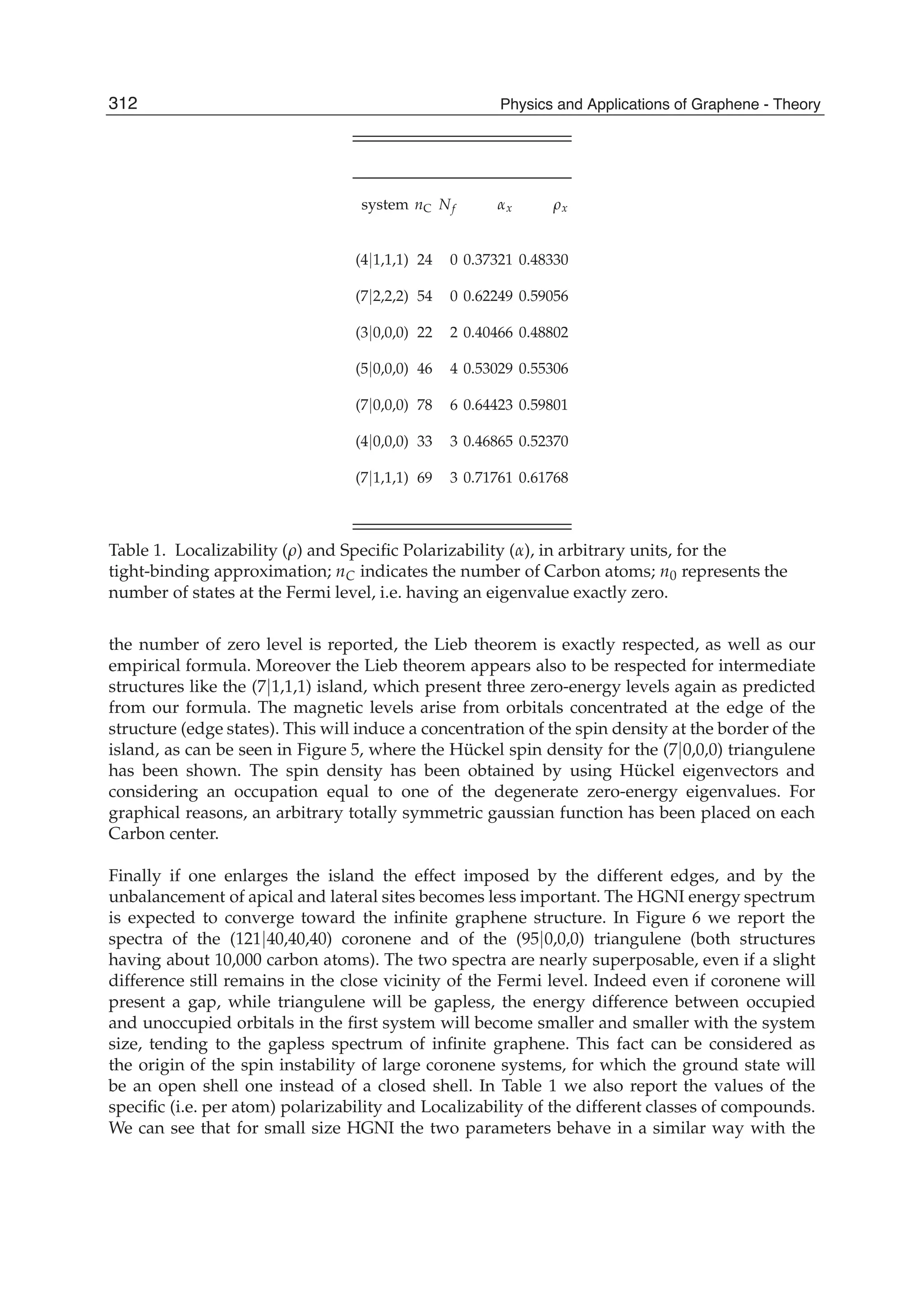
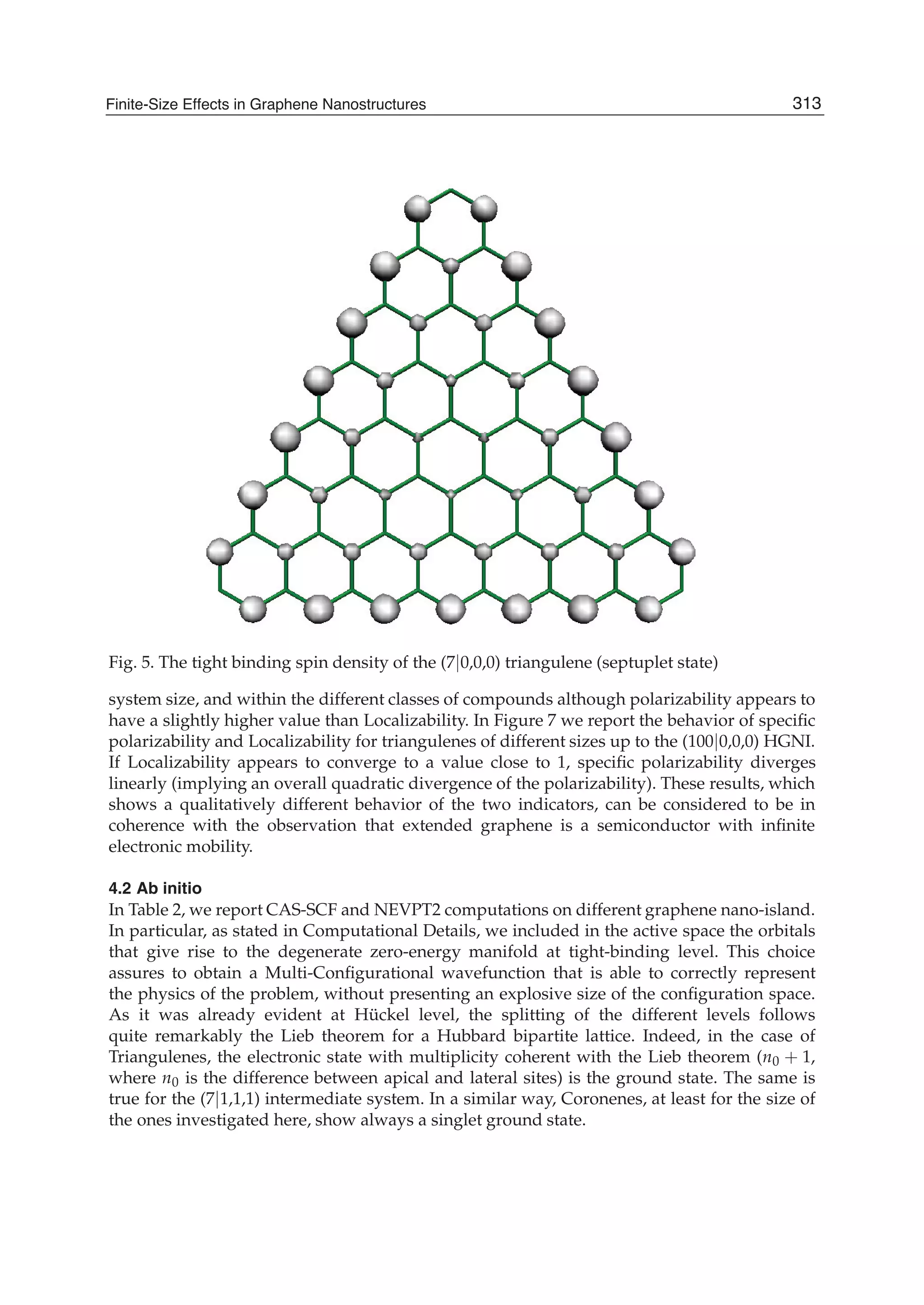
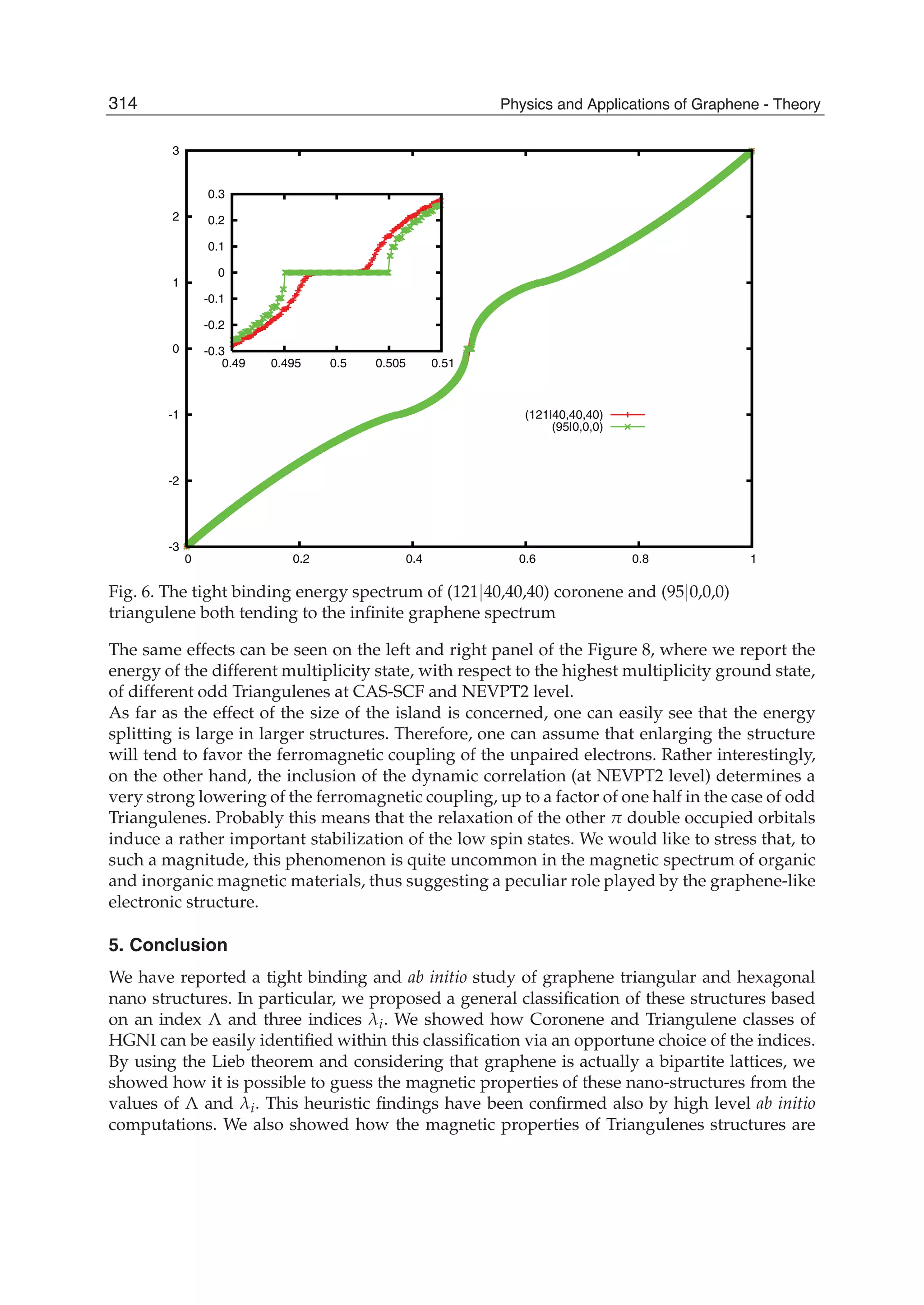
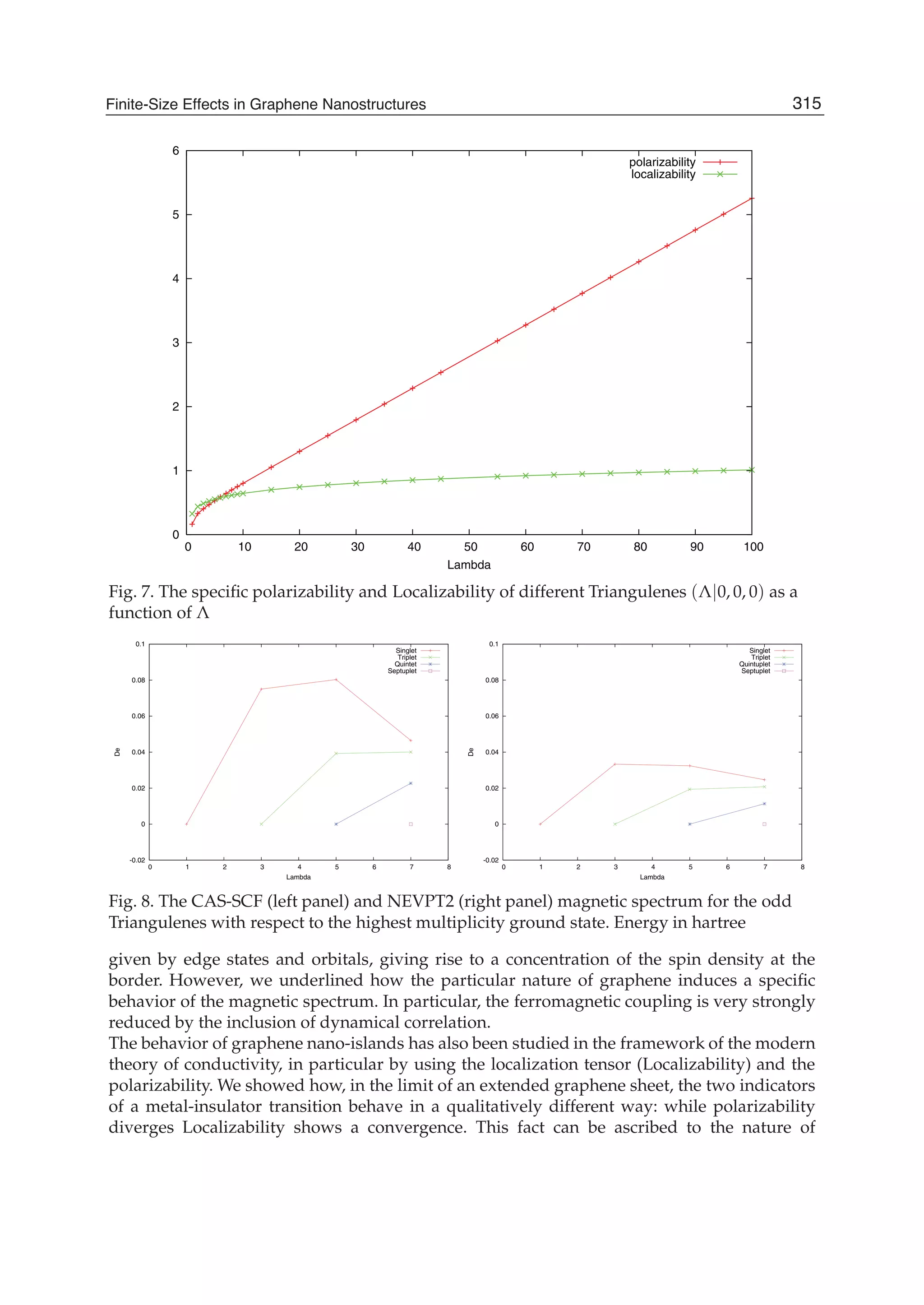
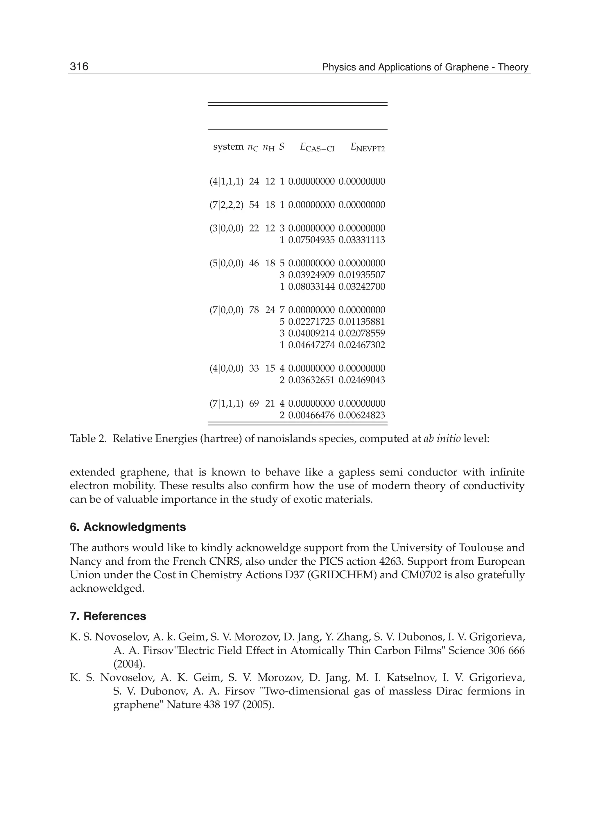
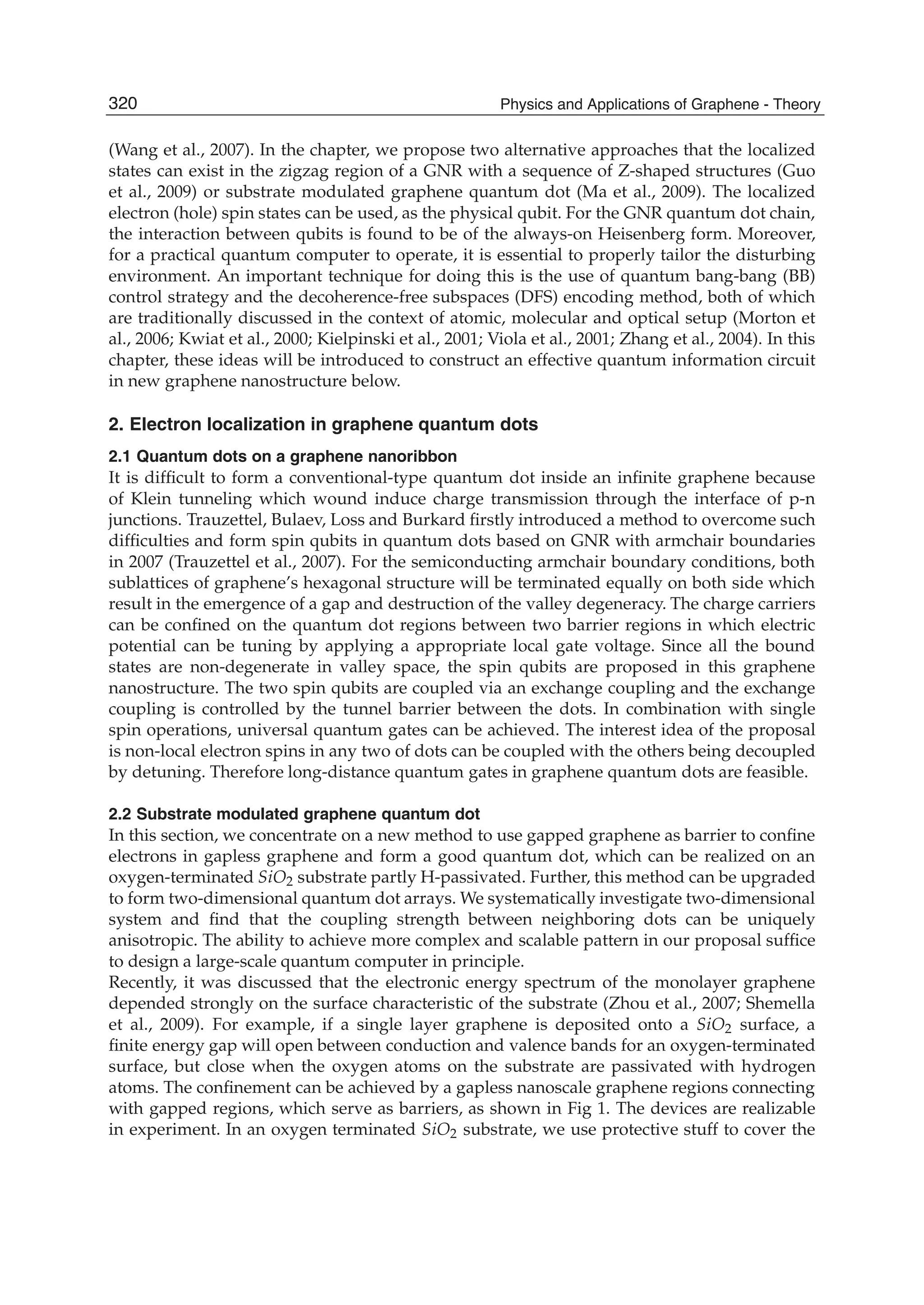
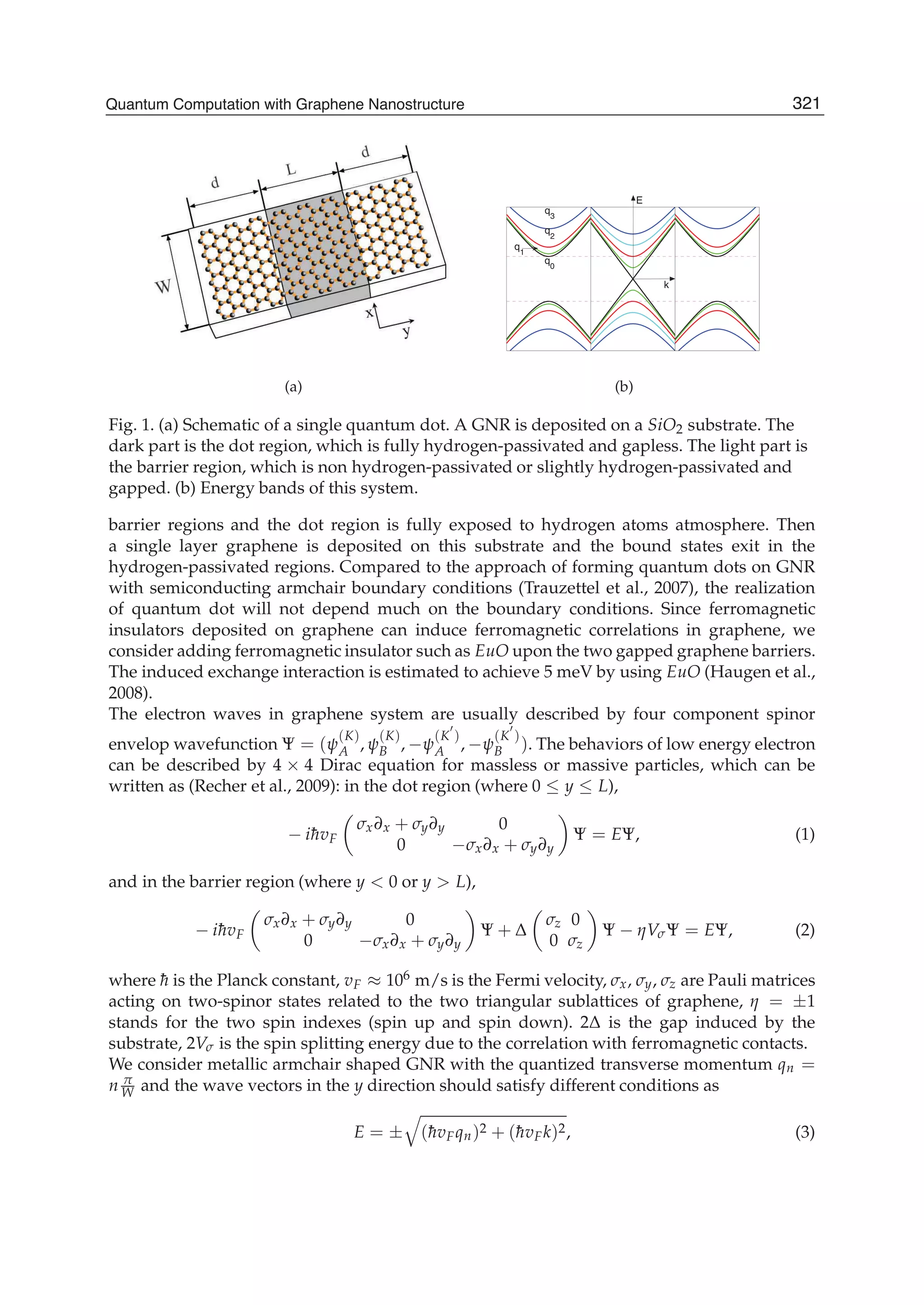
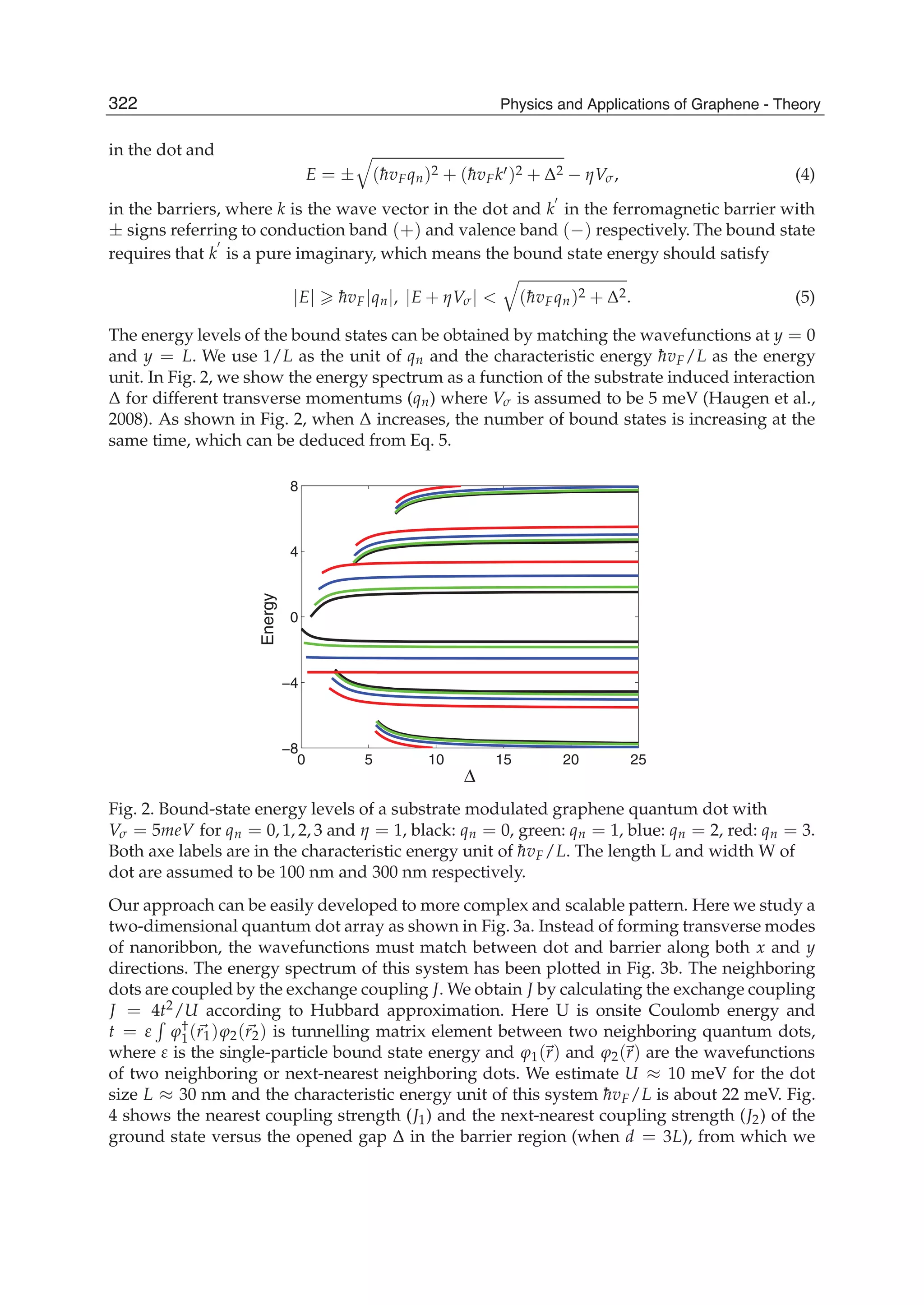
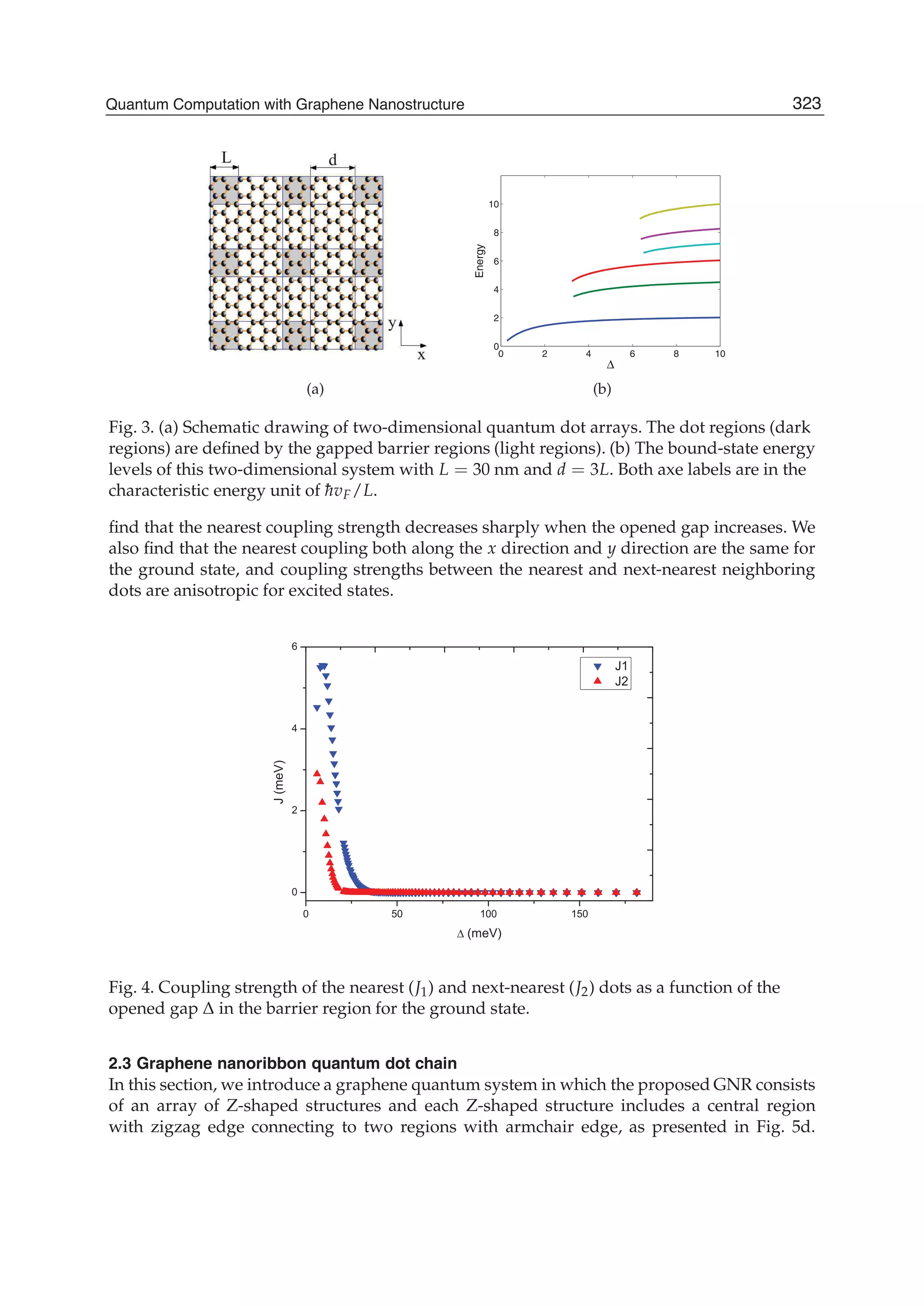
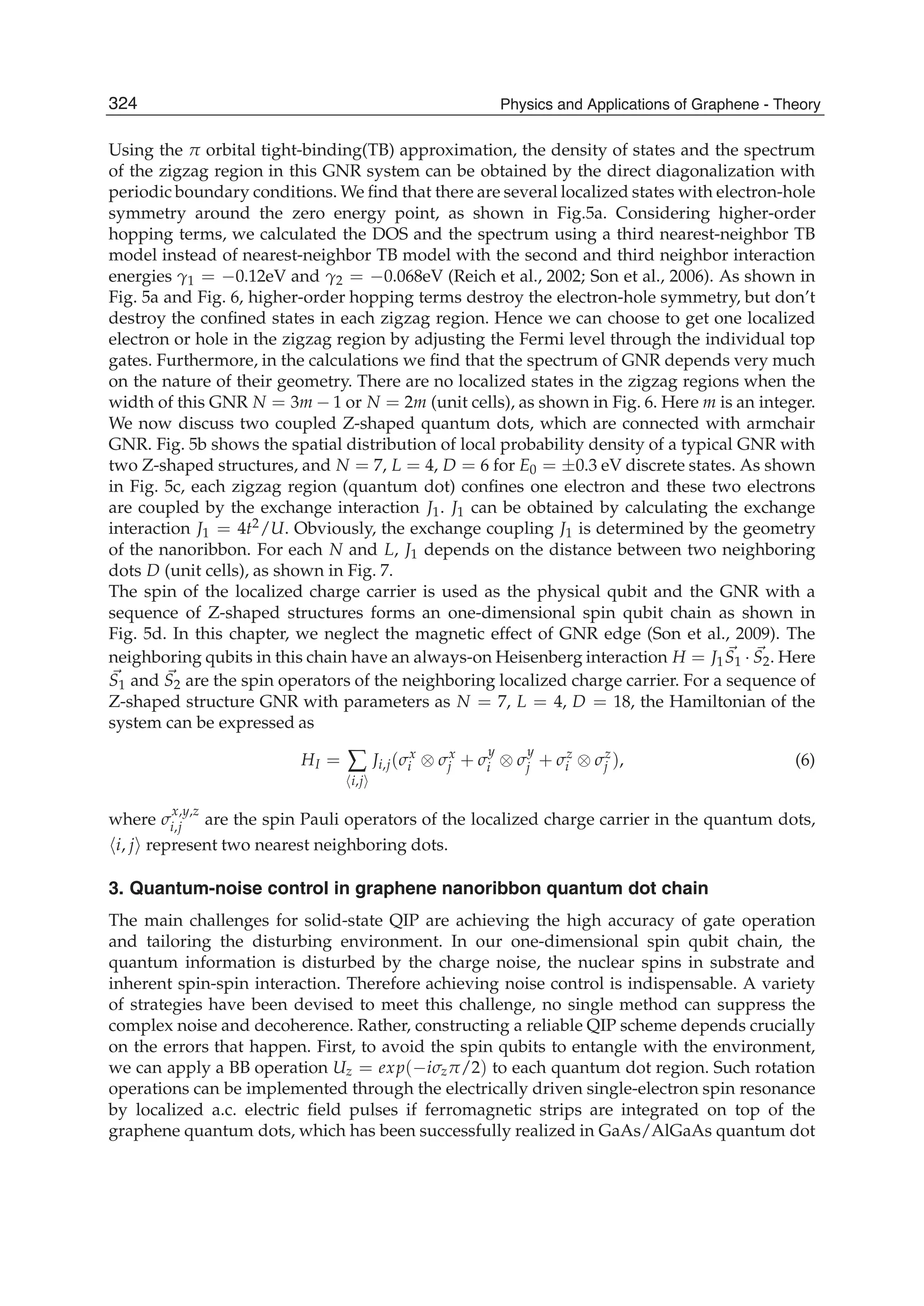
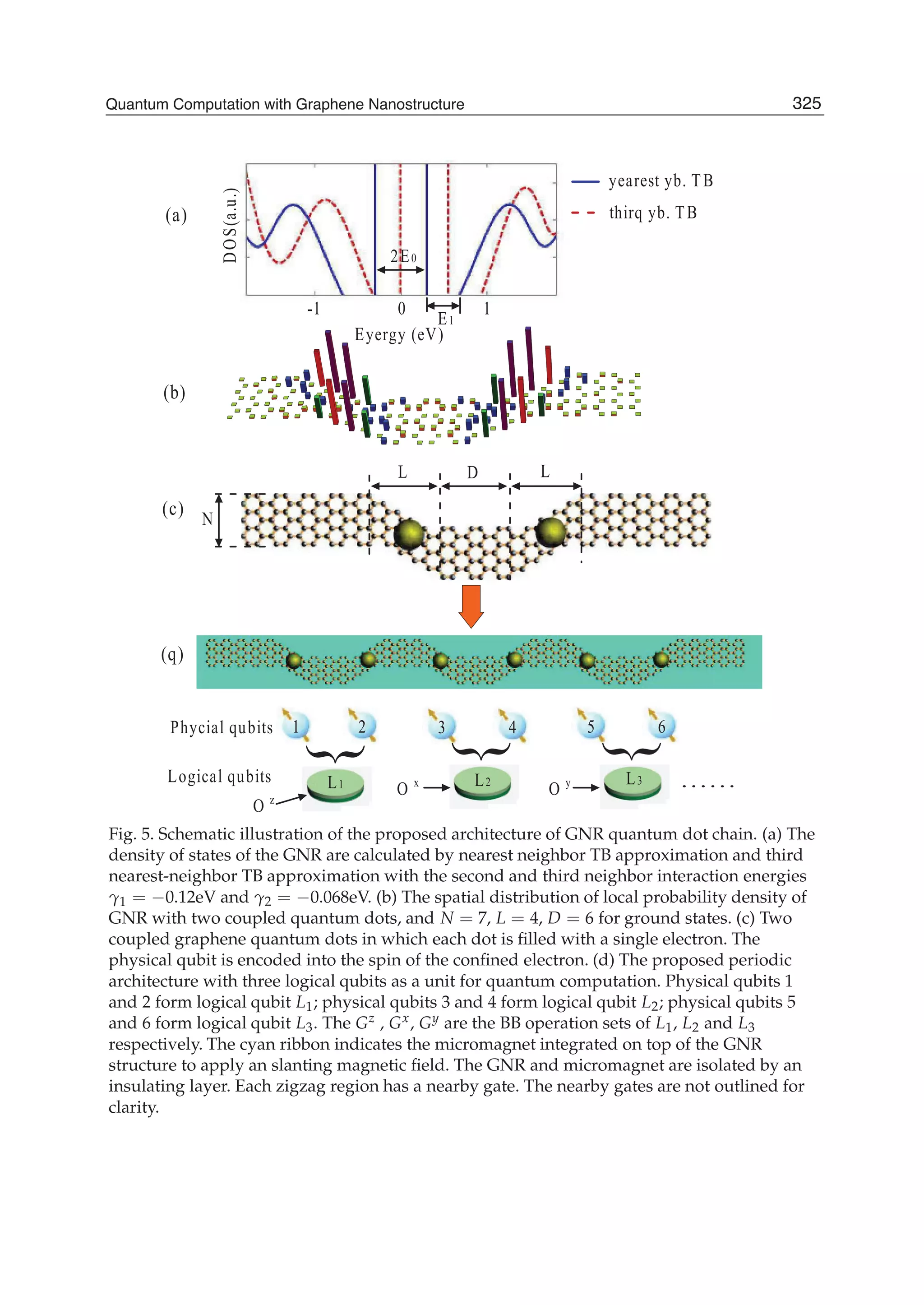
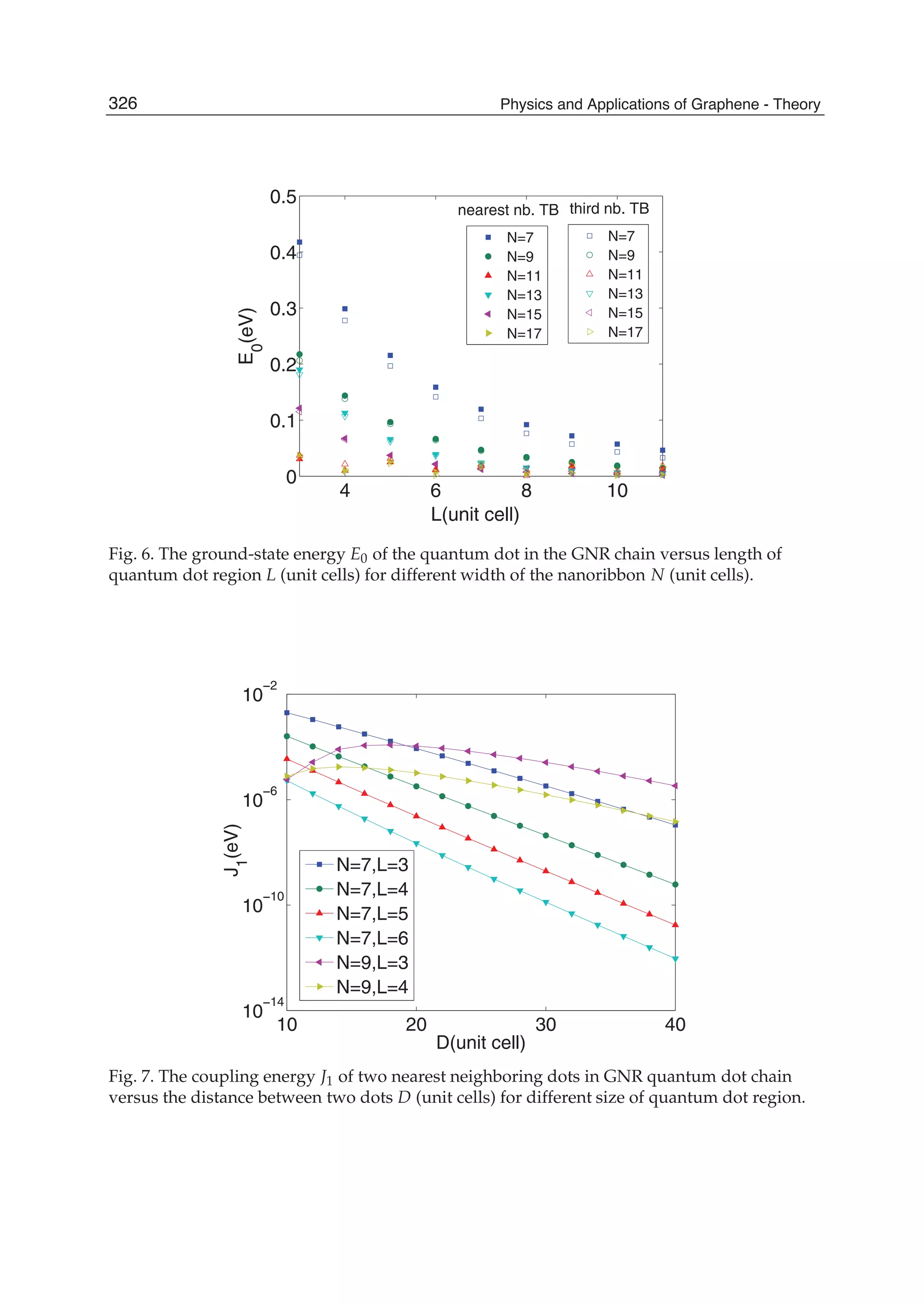
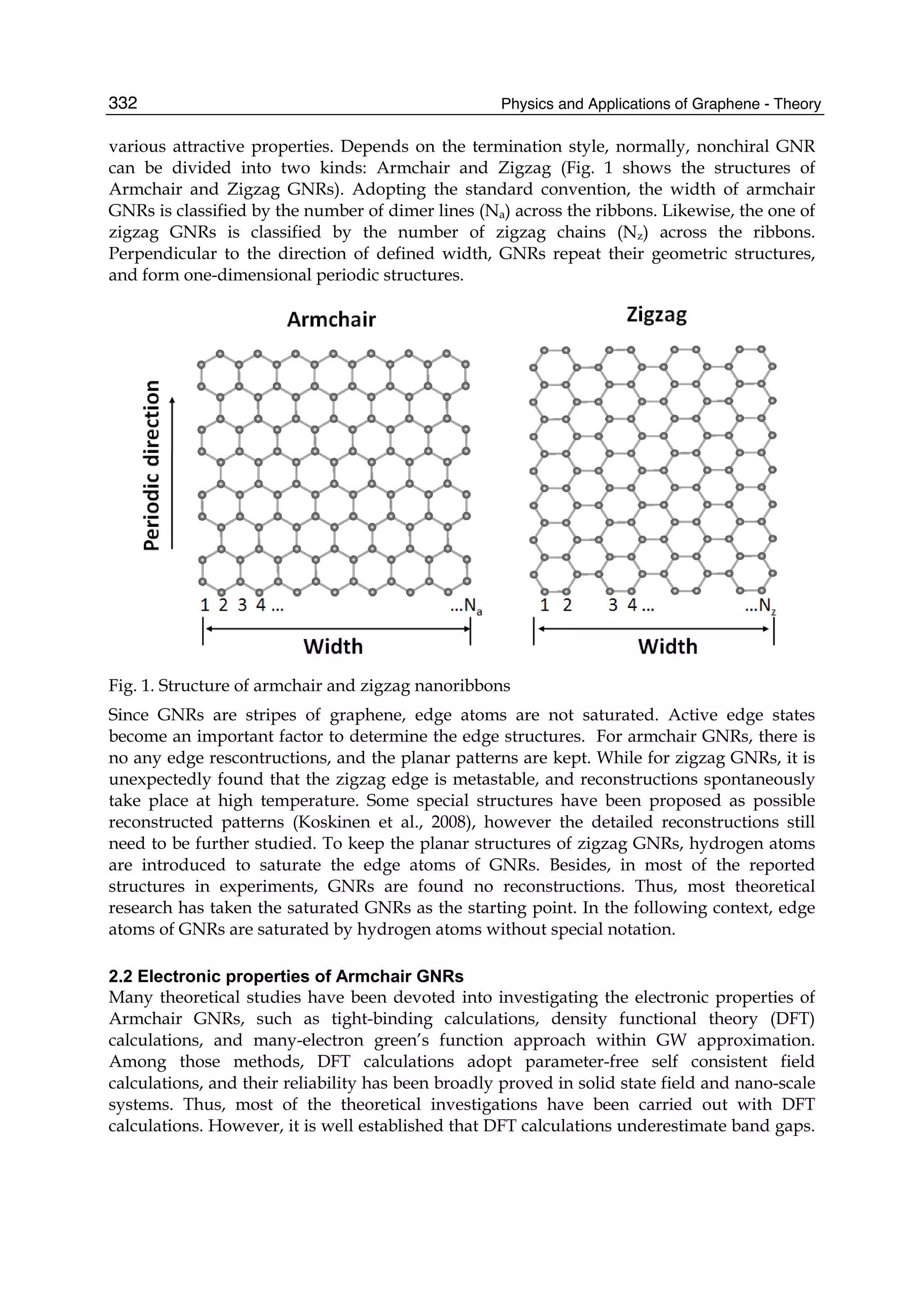
![Graphene Nanoribbons: Geometric, Electronic, and Magnetic Properties 333
Other methods, such GW approximation, have been adopted to correct DFT calculations,
and get the reliable band gaps. In the following discussions, both DFT and GW results are
included.
As shown in the Fig. 1, armchair GNRs are defined by the number of dimer lines (Na) across
the ribbons. Their electronic structures have been carefully investigated by DFT calculations
(Son et al. 2006a). Their results show that all armchair GNRs are semiconductors with
energy gaps, which decrease as a function of increasing ribbon widths. No magnetism has
been found in armchair GNRs. As seen from Fig. 2., the energy gaps as a function of ribbon
width are well separated into three different kinds: Na = 3p, 3p+1, 3p+2 (p is integer).
Moreover, the gap size hierarchy is well separated. Na = 3p+1 categories has the largest
energy gap, while the Na = 3p+2 series is the smallest one.
Fig. 2. The variation of band gaps of armchair GNRs with DFT calculations (Son et al.
2006a).
Armchair GNRs show semiconducting behaviours with a direct energy gap. The
determining factor comes from the quantum confinement effect (QCE), which can be
characterized by [energy gaps] versus [width]-1. Besides the QCE, son et al. has pointed that
the edge effects play an important role to force the armchair GNRs to be semiconductors
(Son et al. 2006a). As discussed in the previous parts, the edge carbon atoms of armchair
GNRs are passivated by hydrogen atoms, which leads to the bonding of carbon atoms at the
edges different with other carbon atoms. As a consequence, the bond lengths of carbon
atoms at the edges are shorter than that in the middle of ribbons, and open the energy gaps
of armchair GNRs.
Although armchair GNRs have three typical families (corresponding to Na = 3p, 3p+1, 3p+2,
respectively) with distinguished energy gaps, they have similar band shapes. As an
example, the band structure of armchair GNR with Na = 13 is shown in Fig. 3. (Sun et al.
2008), there are four important subbands which dominate the electronic behaviors of
armchair GNRs. These subbands are constituted by the π bonds of carbon atoms, and have
different shapes, which provide the possibility of external modulations, such as strain.
On the other hand, although DFT calculations can provide the correct qualitative pictures,
the accurate energy gaps of armchair GNRs are needed. To solve the band-gap problems, Li
et al. have performed first-principles calculations using many-electron Green’s function
approach within the GW approximation, which is treated as one of the most accurate
methods to predict the energy gaps. It is clear that GW calculations give the same hierarchy](https://image.slidesharecdn.com/grrphysicsandapplicationsofgraphene-theory-140422181144-phpapp02/75/physics-and_applications_of_graphene_-_theory-343-2048.jpg)
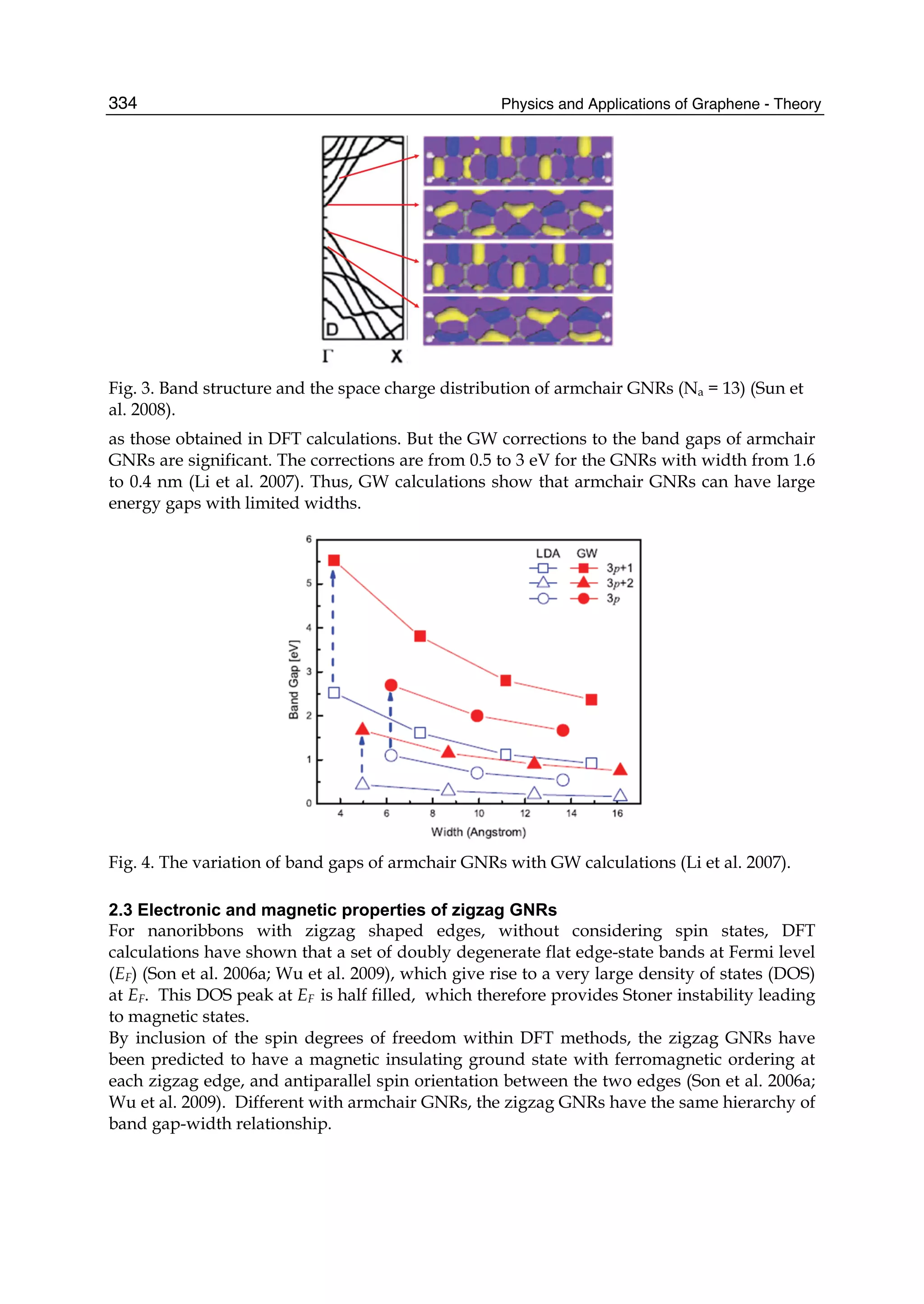
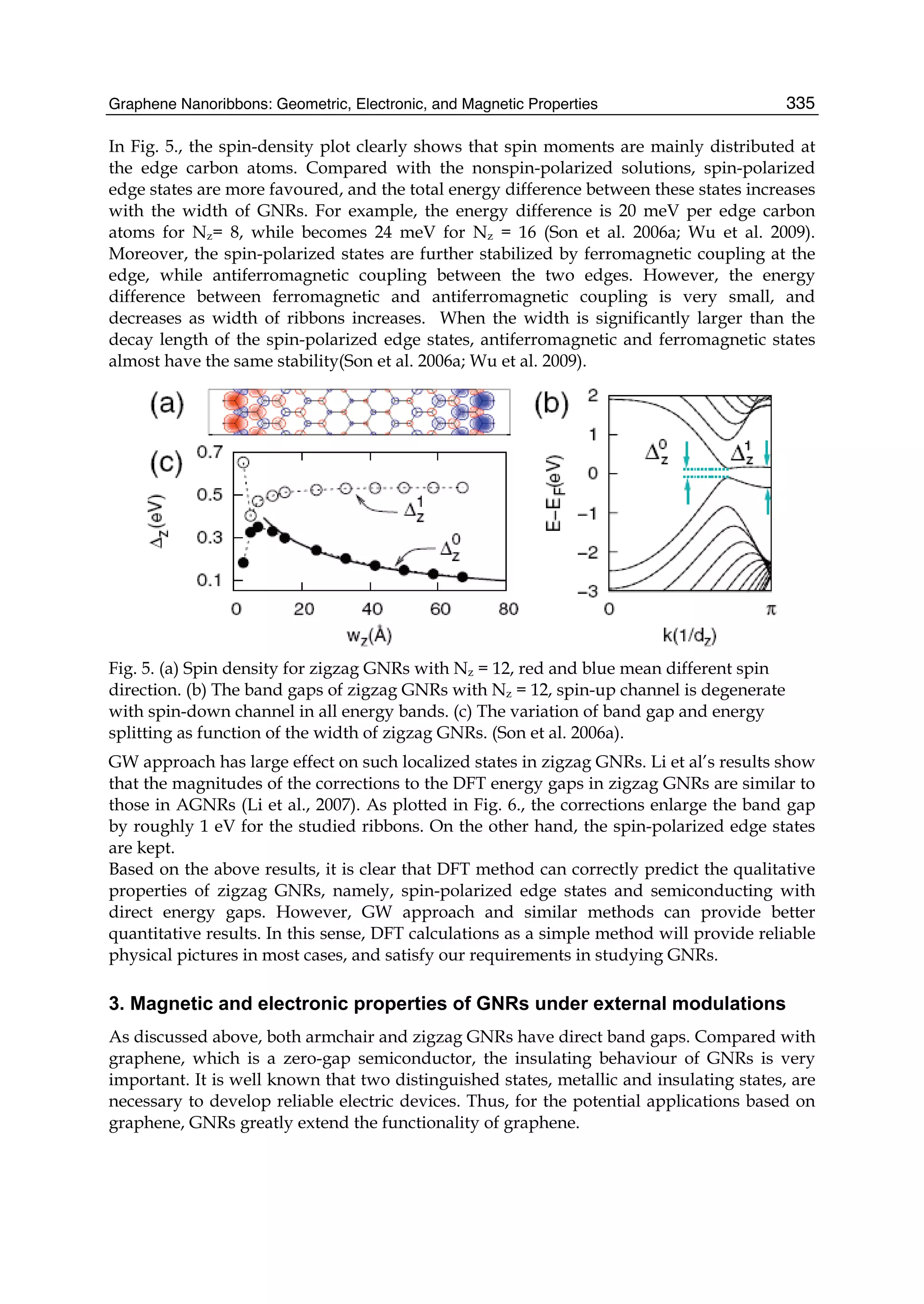
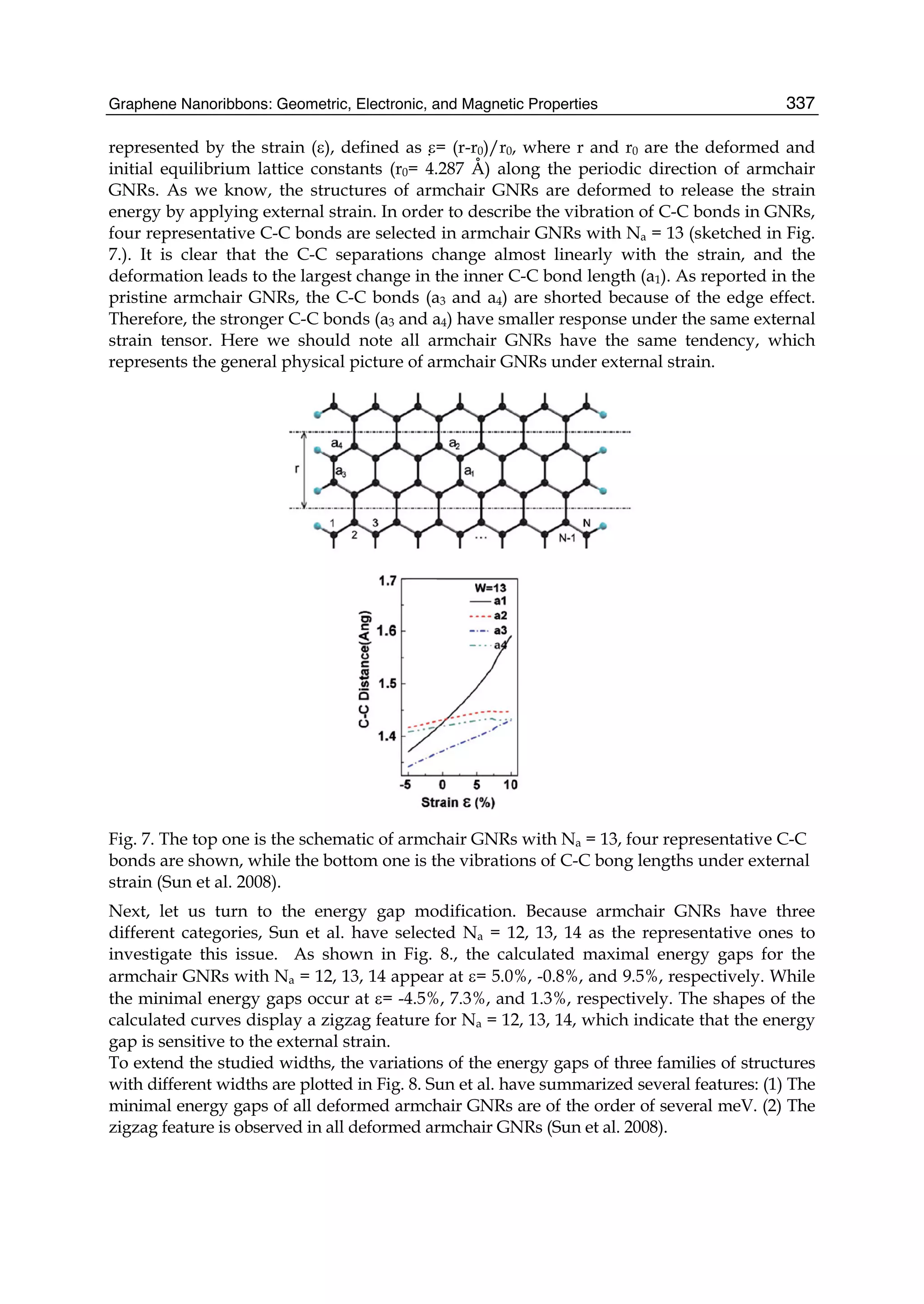
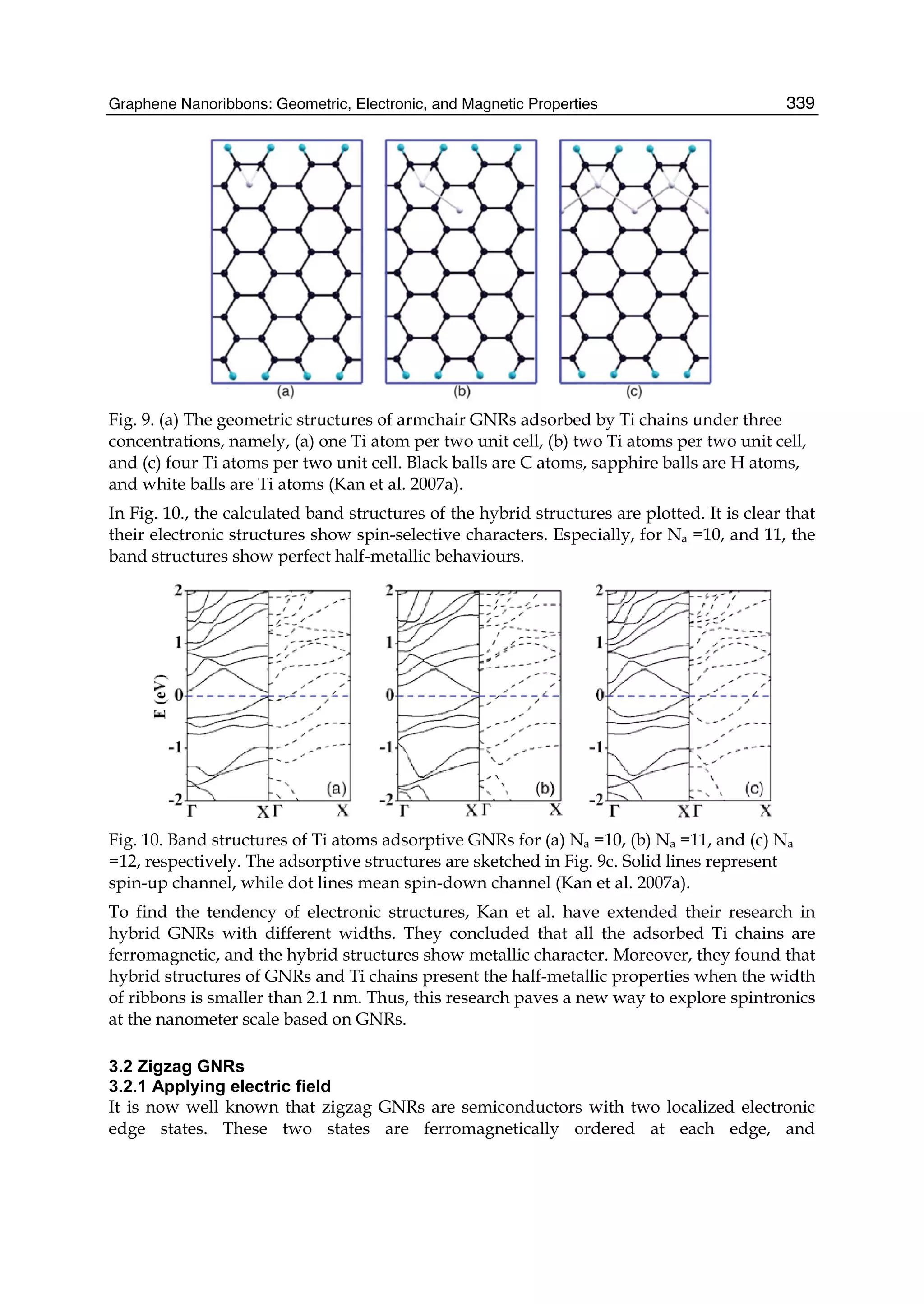
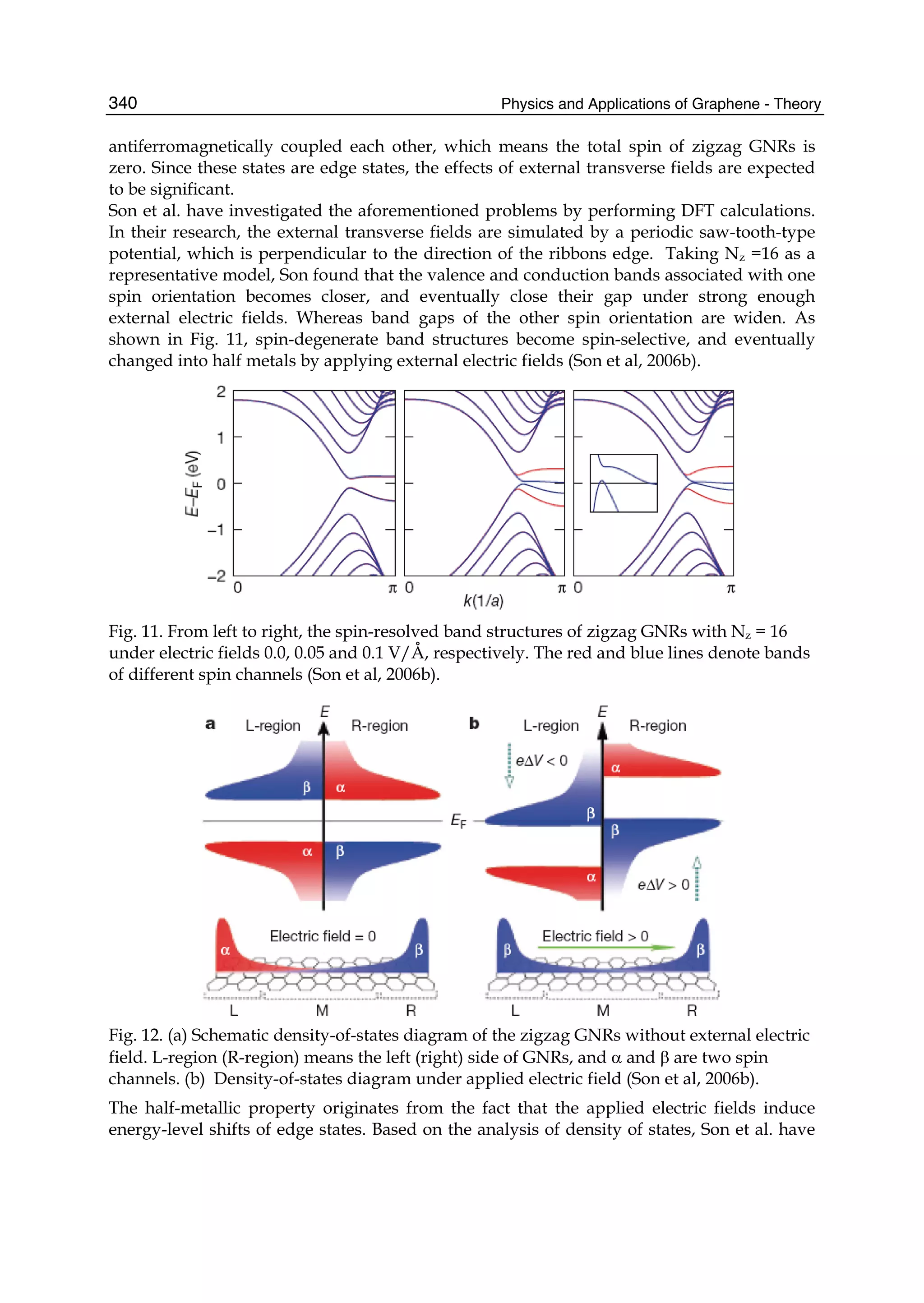
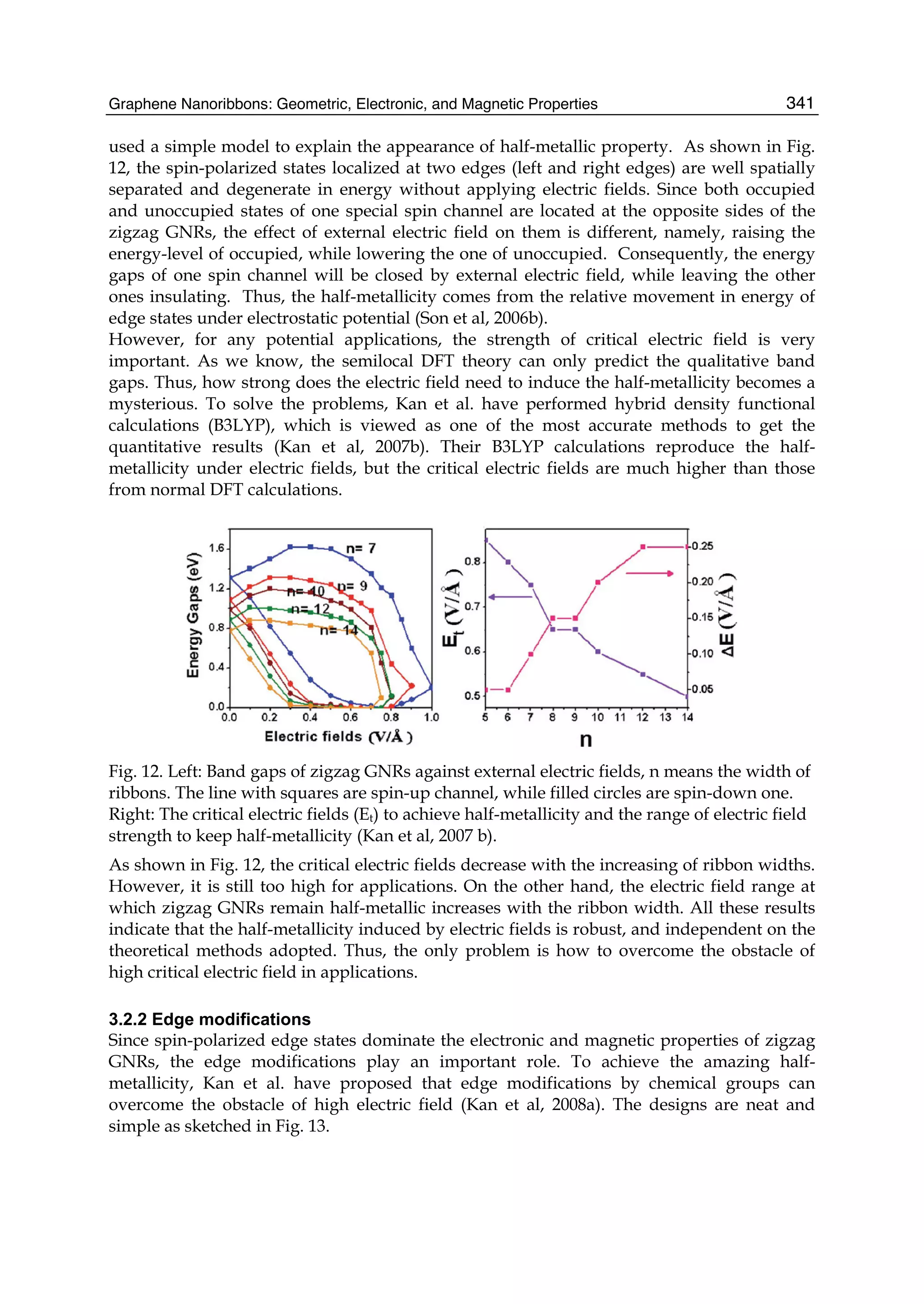
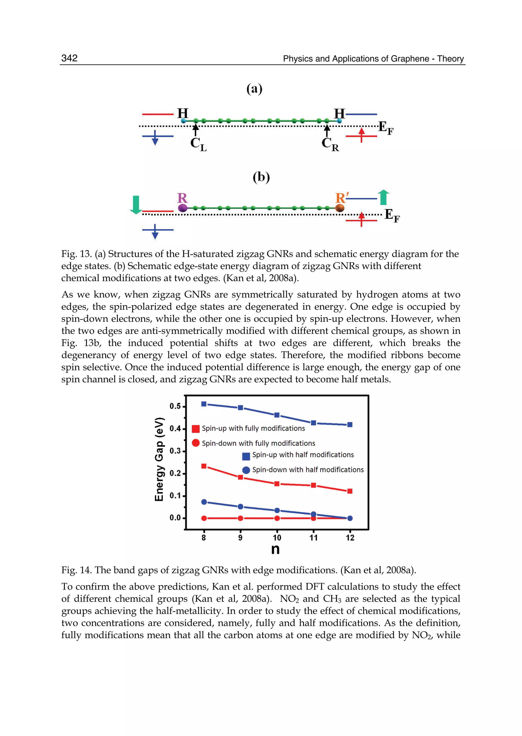
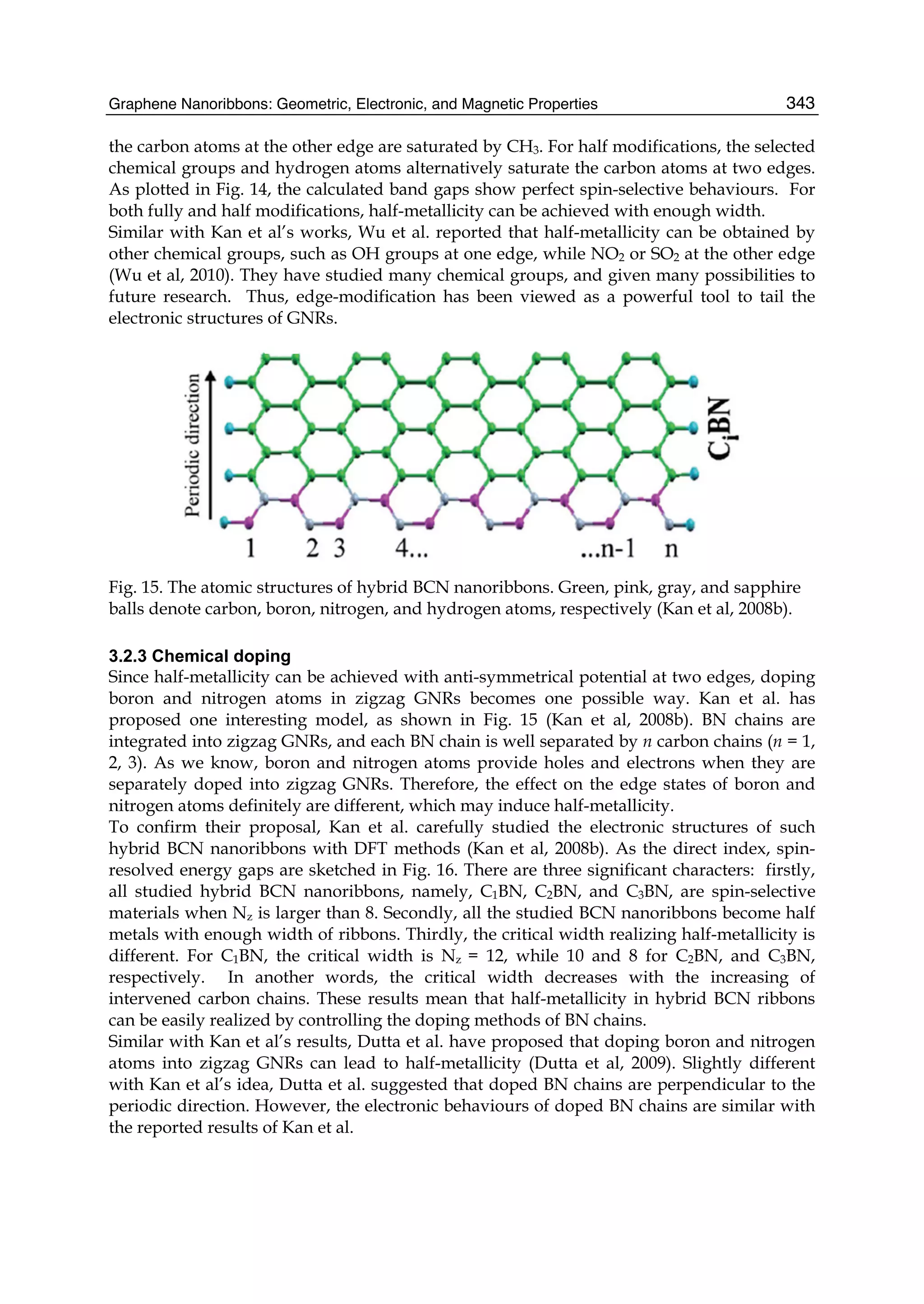
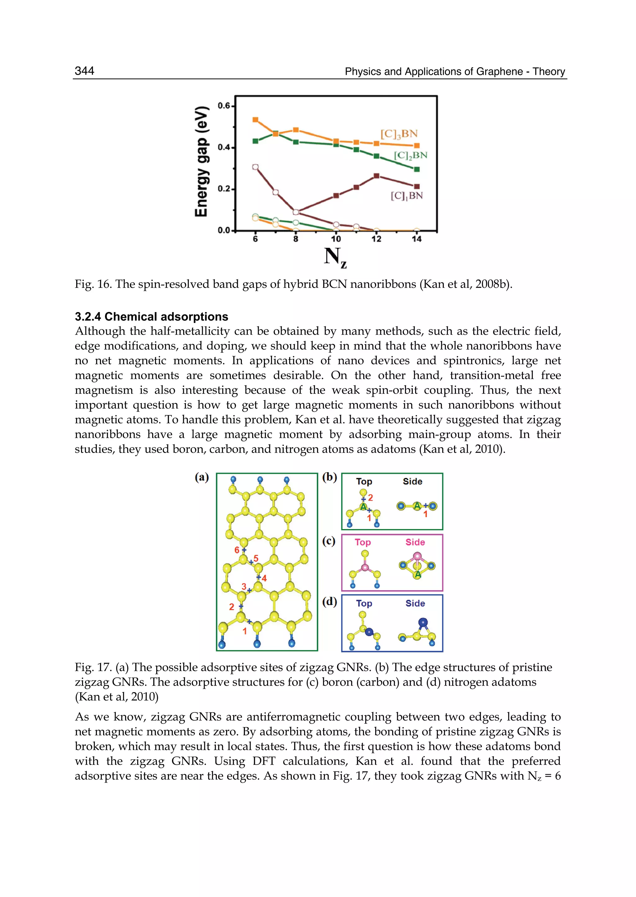
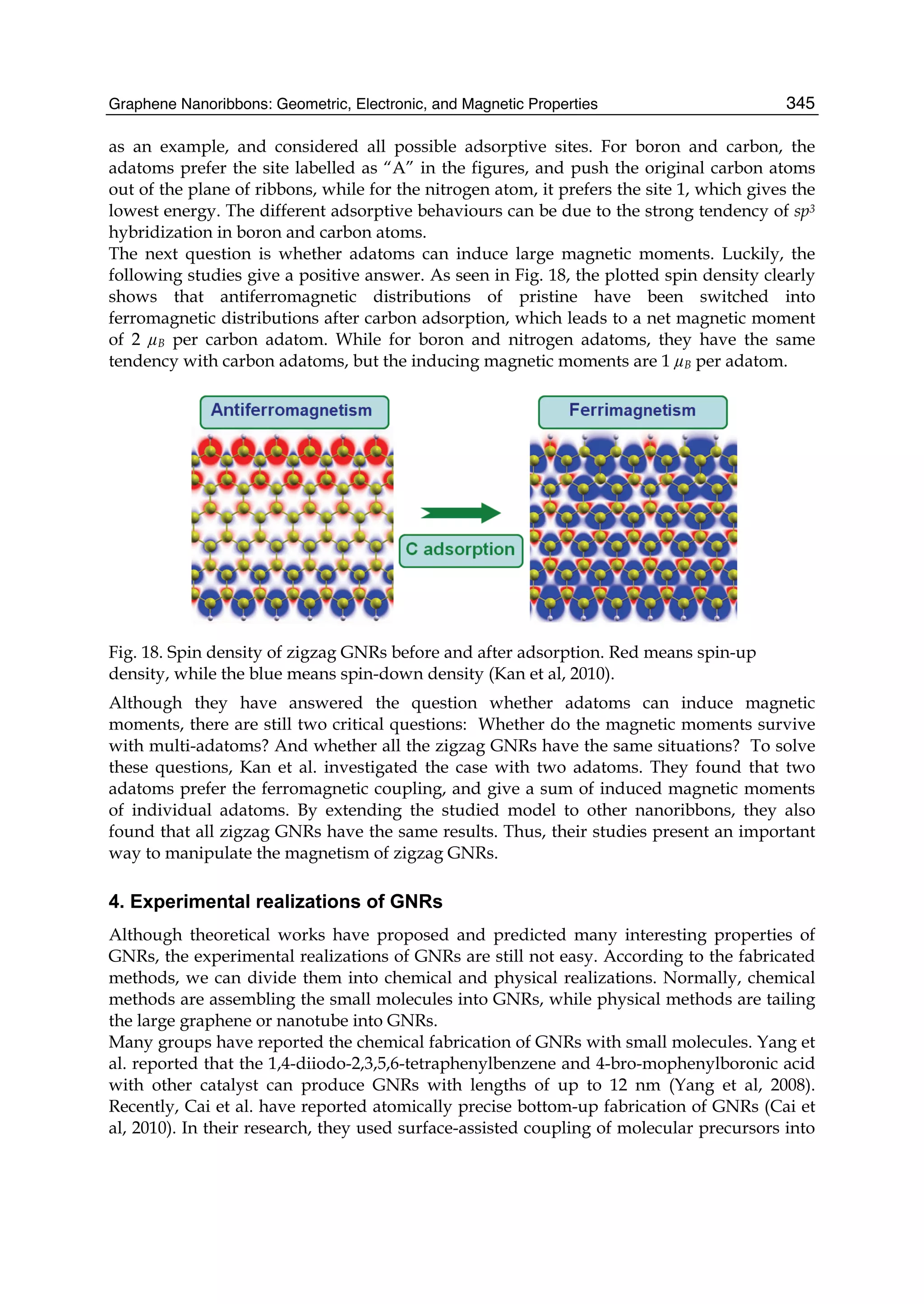
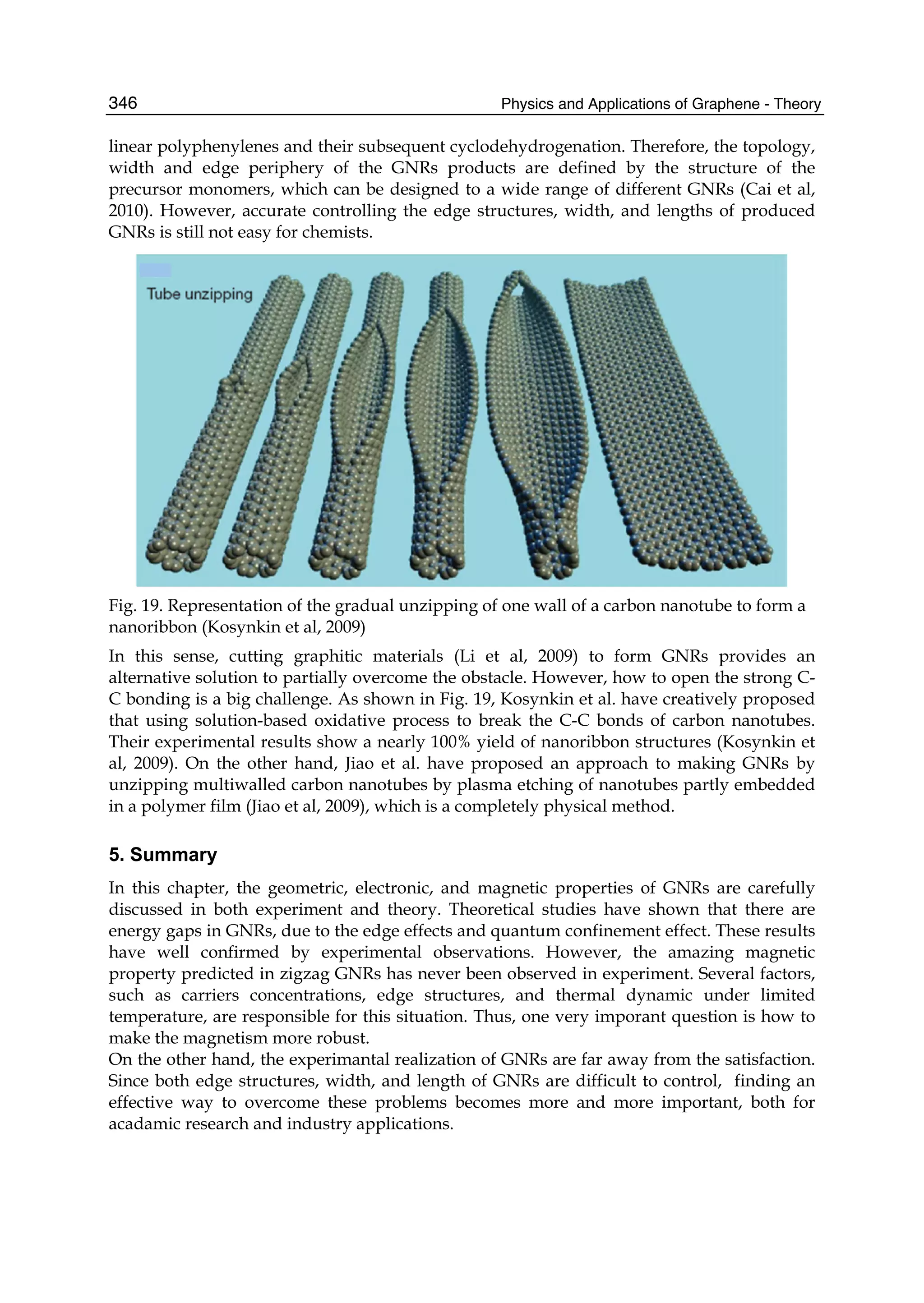

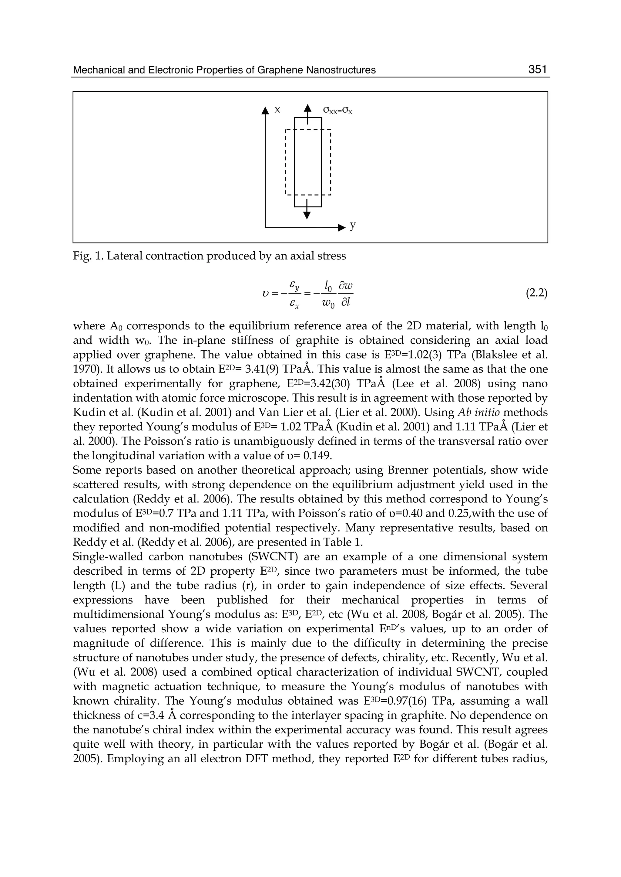
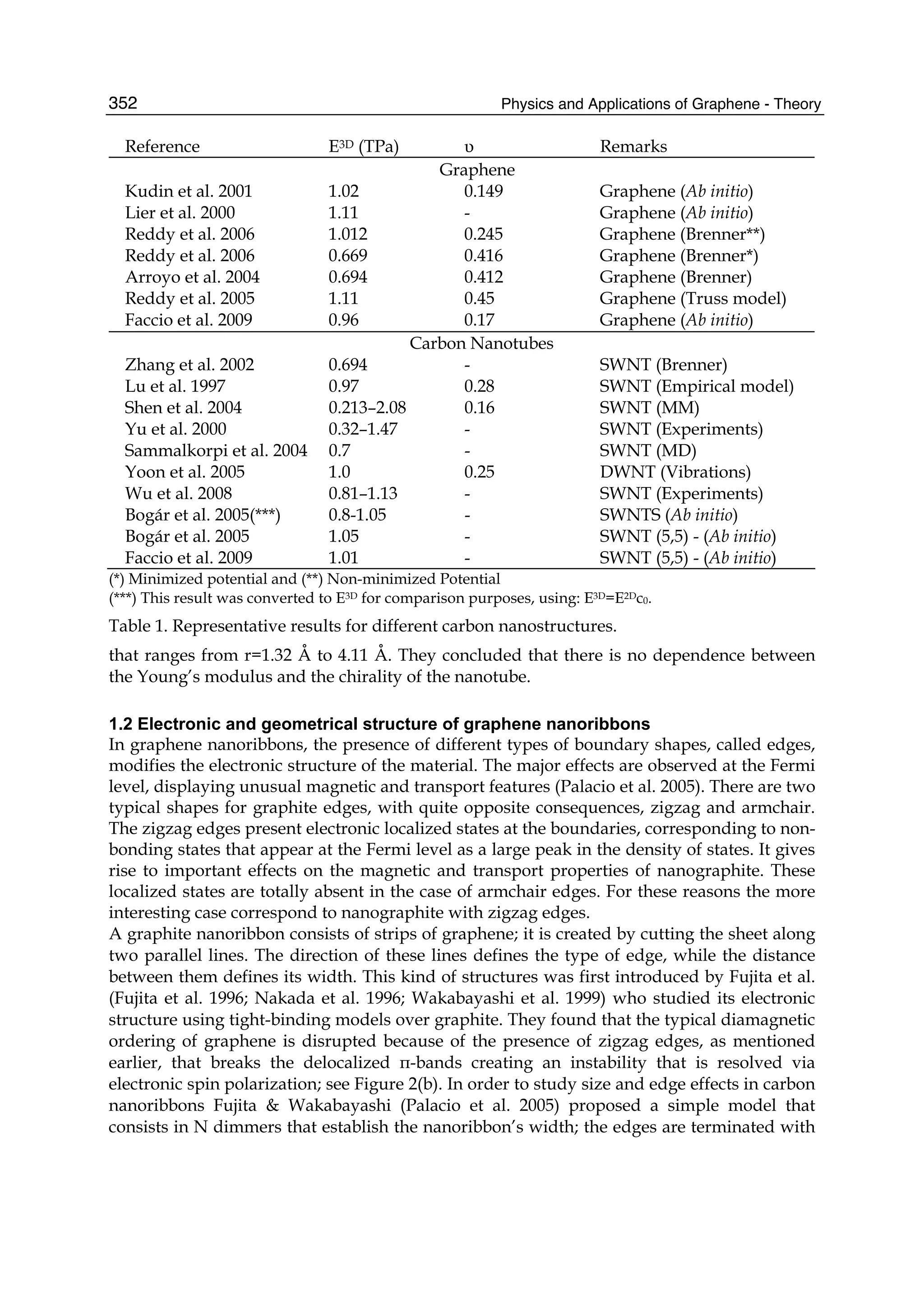
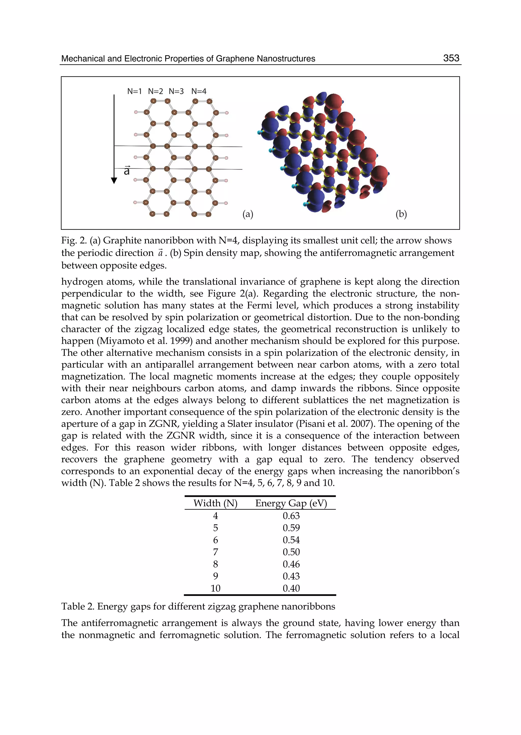
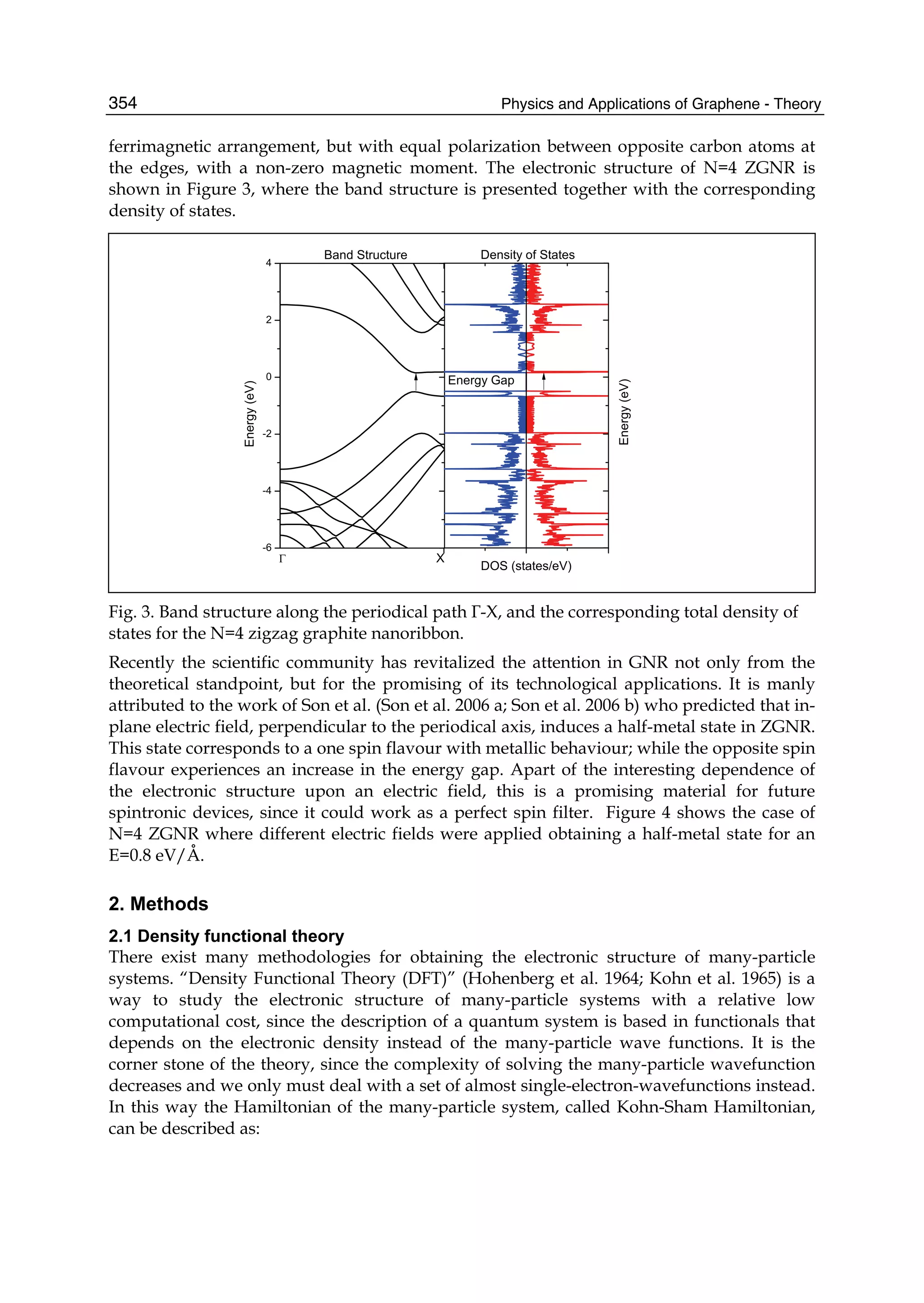
![Mechanical and Electronic Properties of Graphene Nanostructures 355
[ ] [ ] [ ] [ ] [ ]0 ee xc extE T V V Vρ ρ ρ ρ ρ= + + + (3.1)
where T0 corresponds to the kinetic energy functional, Vee is the inter-electronic repulsion,
Vext is the external potential coming from the nucleus arrangement, and finally Vxc is the
exchange and correlation potential. While T0, VH and Vext can be easily incorporated in the
Hamiltonian, since they are well know because of its universal expressions, the Vxc is not
known in an exact form and must be estimated or approximated.
[ ] [ ] [ ] [ ] [ ]0 ee xc extE T V V Vρ ρ ρ ρ ρ= + + + (3.2)
The exchange and correlation effects must be incorporated in the equations because the
universal functionals T0 and Vee do not take into account the fermionic behaviour of the
electronic wavefunction, and fail to describe instantaneously electron-electron interactions,
and it is attributed to the mean field form of the handled expressions. This justifies the
incorporation of an additional term into the Hamiltonian, called the exchange-correlation
potential Vxc, with the purpose to deal with the limitations early mentioned.
The incorporation of the Vxc term represents an additional problem, since there is no
knowledge about the exact form of the functional and approximations should be made in
order to estimate its value.
Fig. 4. Density of states for N=4 ZGNR under different applied electric fields (a) 0.2 V/Å, (b)
0.4 V/Å and (c) 0.8 V/Å.
2.2 Exchange-correlation functionals and dispersive interactions
The last section described the philosophy behind DFT and the origin of the exchange-
correlation potential (xc-potential). The first and most widely used xc-potential is the so
called “Local Density Approximation (LDA)” introduced by W. Kohn and L. J. Sham. The
model assumes that the exchange-correlation energy of a particular density ρ(r) can be](https://image.slidesharecdn.com/grrphysicsandapplicationsofgraphene-theory-140422181144-phpapp02/75/physics-and_applications_of_graphene_-_theory-365-2048.jpg)
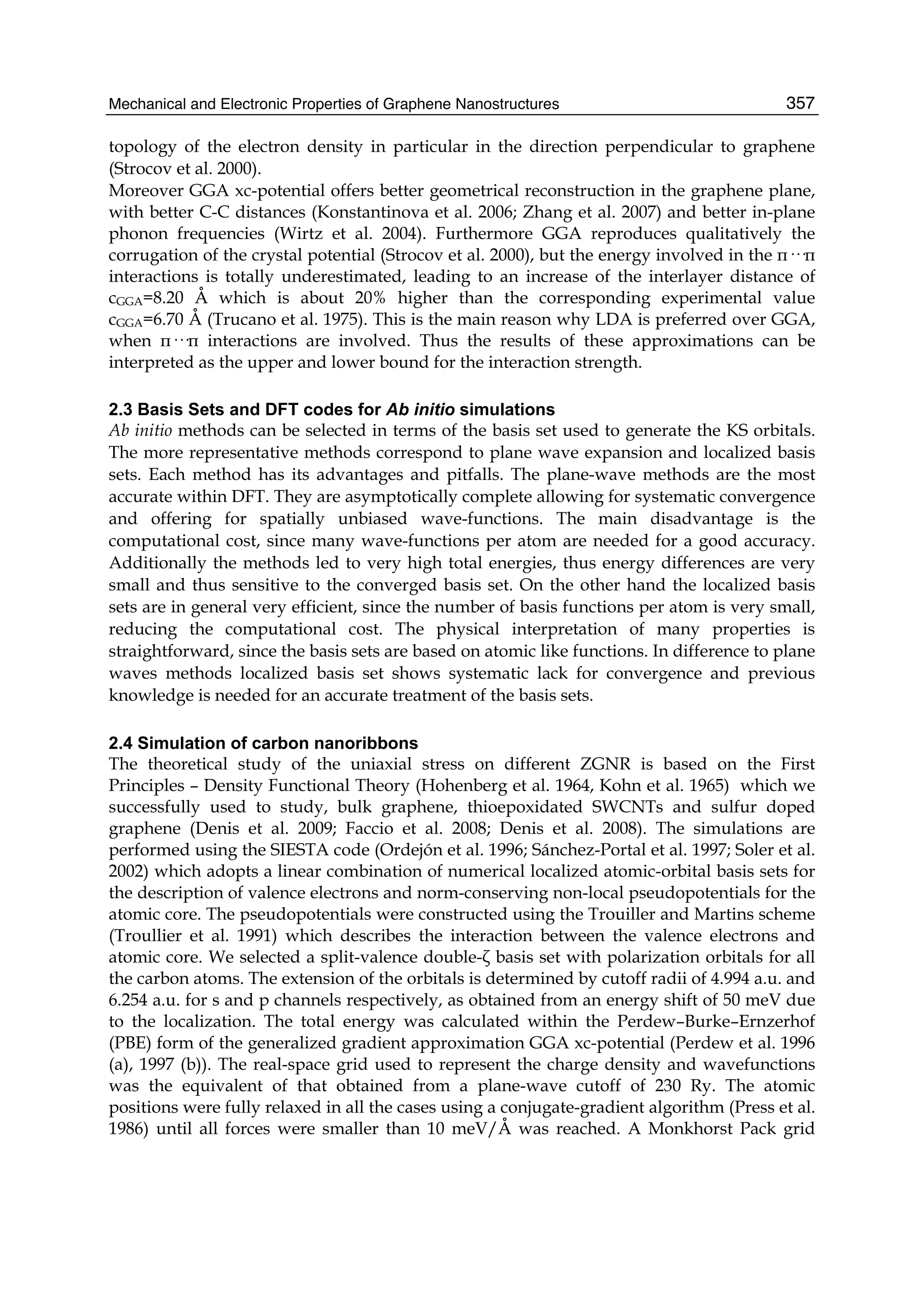
![Physics and Applications of Graphene - Theory358
(Monkhorst et al. 1976) of 300x2x2 supercell, defined in terms of the actual supercell, was
selected to obtain a mesh of 600 k-points in the full Brillouin Zone. All these parameters
allow the convergence of the total energy. In order to validate our methodology we
calculated the Young’s modulus of (5,5) SWCNT, for which the literature shows several
results from Ab initio methods (see Table 1). The smallest unit cell contains a total of 20
carbon atoms. With the purpose to study the dependence on the number of carbon atoms,
we simulated the case 40 carbon atoms per unit cell. The Young’s modulus obtained are
E3D=1.03(2) and E3D=1.01(3) TPa, for 20 and 40 carbon atoms in the unit cell respectively. The
results are consistent within the uncertainty which was estimated from the variance
obtained from the adjustment of the second order fitting of the energy upon unitary
deformation. Therefore one can conclude that the results are not affected by the number of
supercells used, in particular along the periodic direction. Additionally the results are in
good agreement with the reported in the bibliography see Table 1, in particular with an
excellent agreement with those from Bogár et al. (Bogár et al. 2005). Regarding geometry in
graphene nanoribbons, we can distinguish two C-C bond orientations: the bond
perpendicular to the crystalline periodic direction d(|) and the bond diagonal to the normal
direction d(/). The bond distances differ from the inner part of the ribbon (bulk) respecting
the atoms at the edge. In the case of bulk C-C distances we found d(|)bulk= 1.44 Å and
d(/)bulk=1.44 Å, while at the edge of the ribbon we found d(|)edge= 1.46 Å, and
d(/)edge=1.43 Å. This result agrees with the tendency observed by Pisani et al. (Pisani et al.
2007), where the perpendicular bond elongates at the edge, contracting the corresponding
diagonal bond at the edge. It promotes an increase of the zigzag C-C-C angle from 120° at
the bulk to 121.9° at the edge. This trend is observed for the whole un-stressed studied
ribbons. For all of these reasons, we can unequivocally conclude that our methodology is
valid.
3. Results and discussion
The selected ZGNR for simulation correspond to N=4, 5, 6, 7, 8, 9 and 10. Since the code
handled was designed for three dimensional materials, we designed special unit cells. All
the cells were orthogonal, with the GNR placed in the ab plane, and oriented with the
periodic direction along the a axis, see Figure 1 for the ZGNR N=4 sketch. In order to avoid
interference between symmetry images, vacuum regions of 15 Å were added along b and c
directions. In the case of the smallest unit cell, the a axis value for every cell is approximately
a0= 2.495 Å, with a total number of atoms of 2N+2. With the purpose of increase the number
of degrees of freedom in each case, the cells were expanded in four units along the a axis
(a=4a0), it allows us to multiply by four the number of atoms inside the supercells according
to 8N+8. The total number of atoms in each case is: 40, 48, 56, 64, 72, 80 and 88. The stress-
strain curves are obtained applying different stress to the GNR, allowing full atomic
relaxation together with full unit cell parameters optimization, until the desired stress tensor
is reached. Since we are considering uniaxial strain only, the Voigt tensor has only one non-
zero component: [σx, σy, σz, σxy, σxz, σyz]→[σx, 0, 0, 0, 0, 0]. The selected stress components of
the Voigt tensor allow us to establish strains in the range of εx= ±0.020 for the whole series,
which assures a linear stress regime (Liu et al. 2007, Khare et al. 2007). It corresponds to a
quadratic dependence of the total energy upon the strain. The most important features of
the data treatment are presented in Figure 5 for N=10 ZGNR.](https://image.slidesharecdn.com/grrphysicsandapplicationsofgraphene-theory-140422181144-phpapp02/75/physics-and_applications_of_graphene_-_theory-368-2048.jpg)
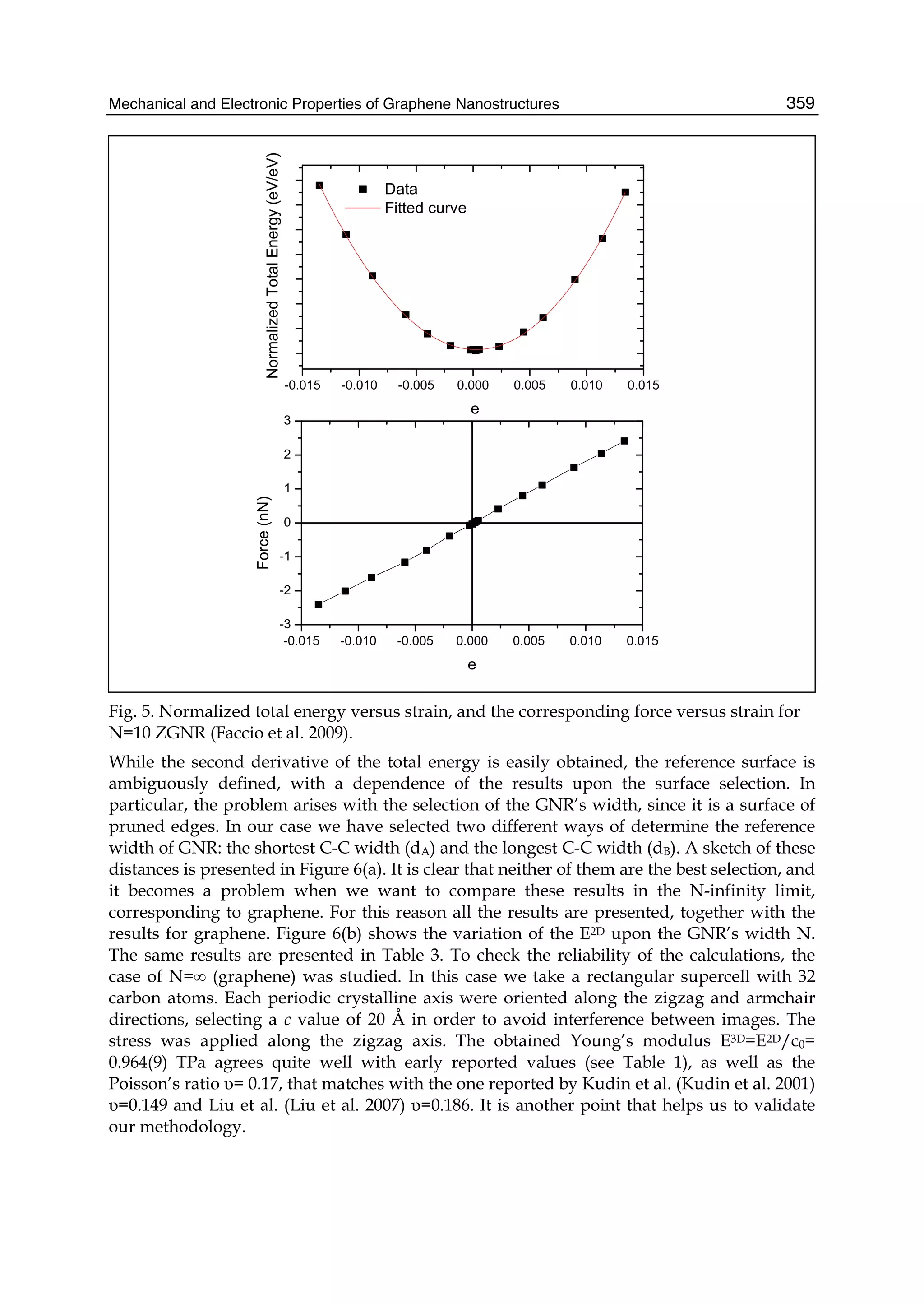
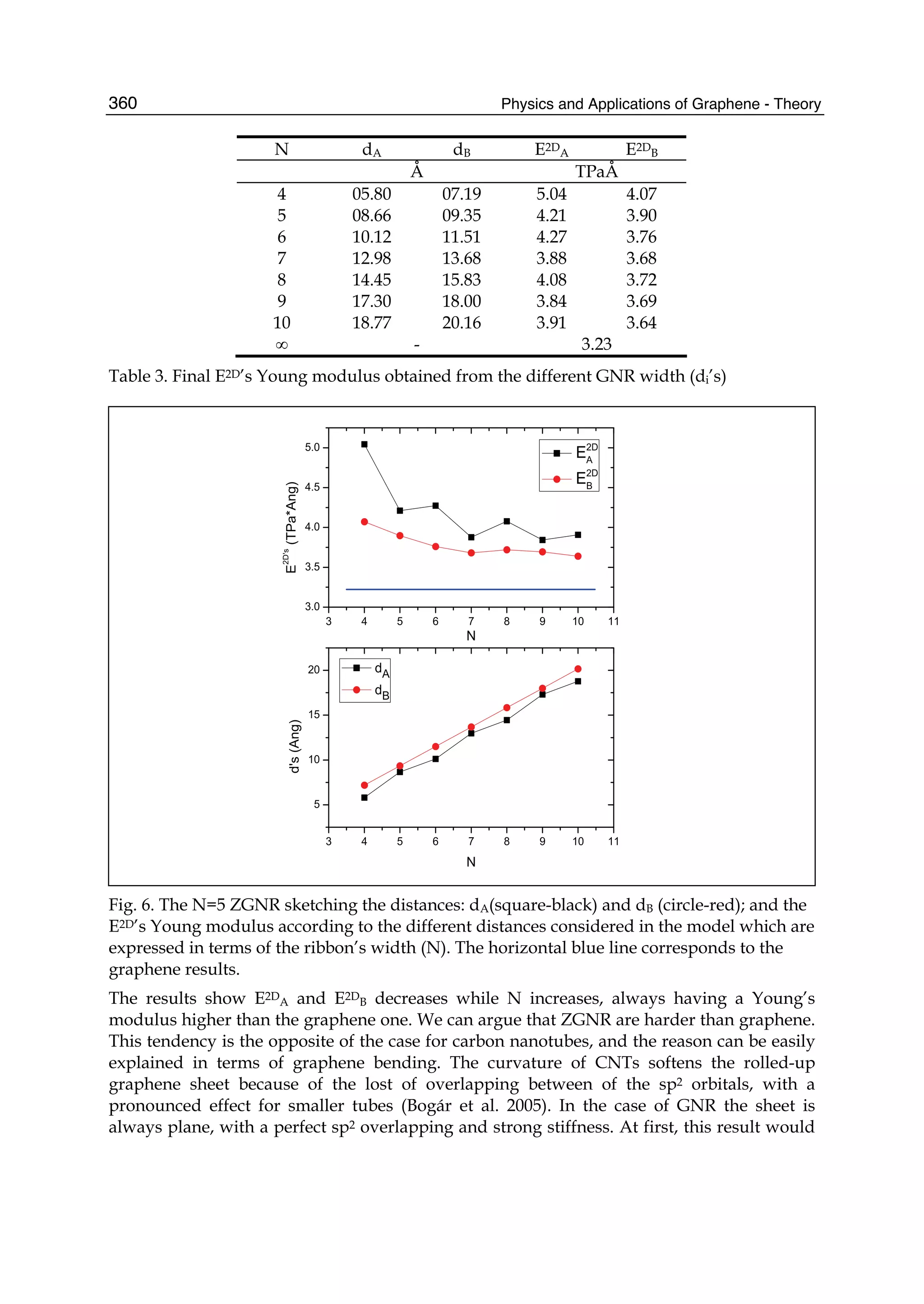
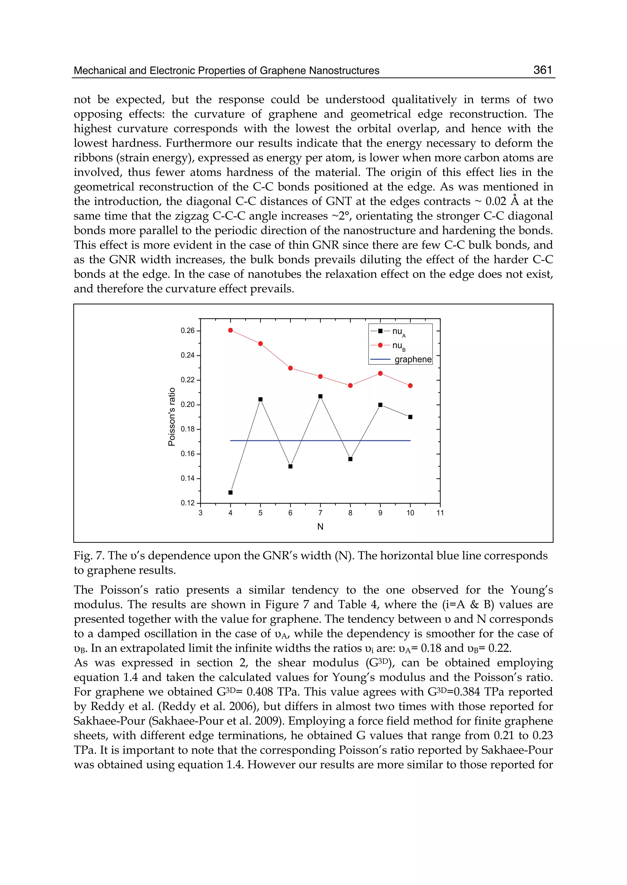
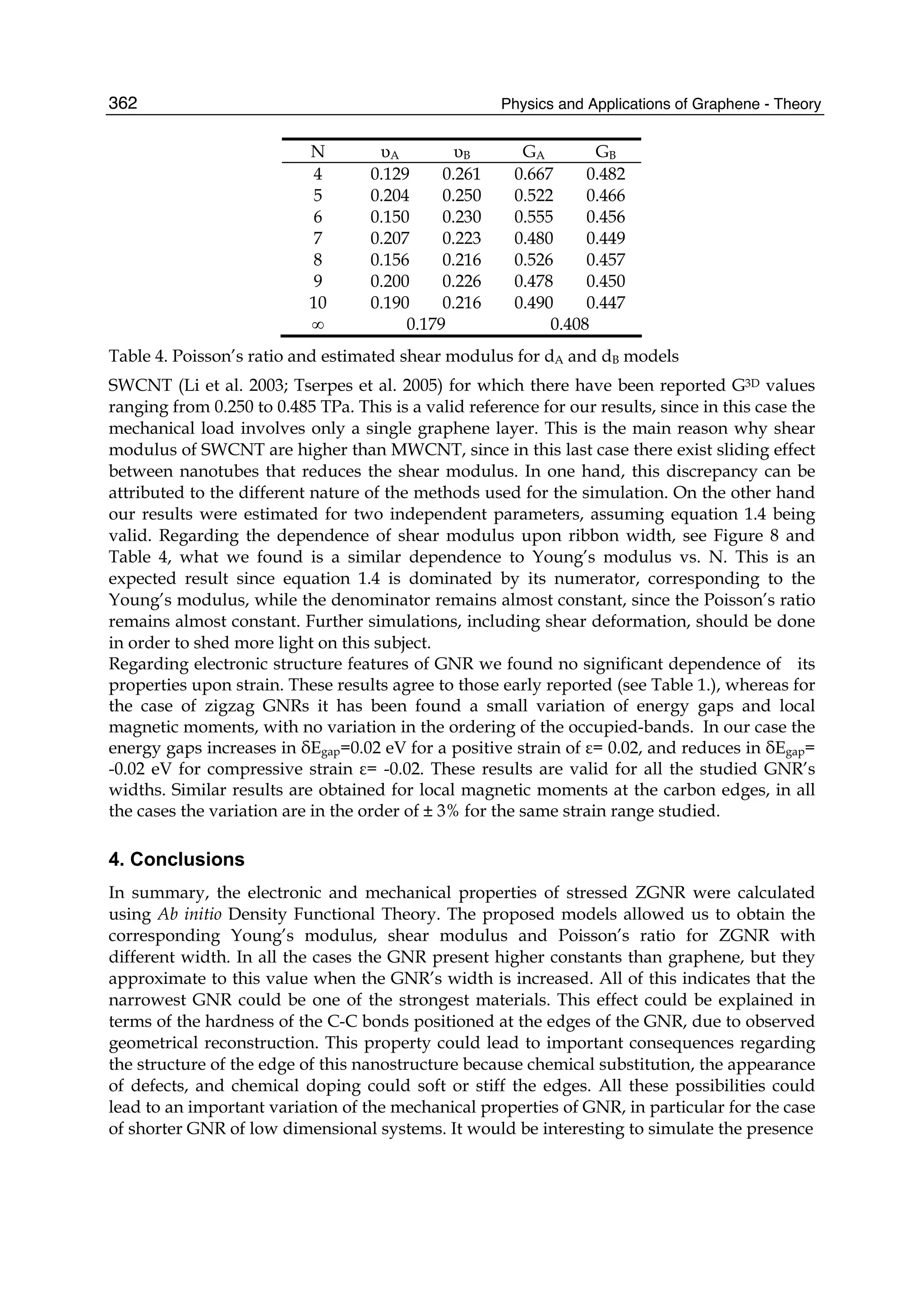
![Mechanical and Electronic Properties of Graphene Nanostructures 365
Lier, G. V.; Alsenoy, C. V.; Doren, V. V. & Greelings, P. (2000). Ab initio Study of the Elastic
Properties of Single-Walled Carbon Nanotubes and Graphene". Chem. Phys. Lett.,
326, 181.
Liu, F.; Ming, P. M. & Li, J. (2007). Ab initio calculation of ideal strength and phonon
instability of graphene under tension. Phys. Rev. B, 76, 064120.
Lu, J. P. (1997). Elastic Properties of Carbon Nanotubes and Nanoropes. Phys. Rev. Lett., 79,
1297-1300.
Miyamoto, Y.; Nakada, K. & Fujita, M. (1999). First-principles study of edge states of H-
terminated graphitic ribbons. Phys. Rev. B, 59, 9859.
Monkhorst, H. J. & Pack, J. D. (1976). Special points for Brillouin-zone integrations. Phys.
Rev. B, 13, 5188-5192.
Nakada, K.; Fujita, M.; Dresselhaus, G. & Dresselhaus, M. S. (1996). Edge state in graphene
ribbons: Nanometer size effect and edge shape dependence. Phys. Rev. B, 54, 17954.
Ordejón, P.; Artacho, E. & Soler, J.M. (1996). Self-consistent order-N density-functional
calculations for very large systems. Phys. Rev. B, 53, R10441
Palacio, F. & Makarova, T. (2005). Carbon-based Magnetism, ISBN 13:978.0.444.51947-4,
Elsevier. B. V., Amsterdam, The Netherlands.
Perdew, J. P. and Zunger, A. (1981). Self-interaction correction to density-functional
approximations for many-electron systems. Phys. Rev. B, 23, 5048-5079.
Perdew, J. P.; Burke, K.; and M. Ernzerhof, (1996). Generalized Gradient Approximation
Made Simple. Phys. Rev. Lett., 77, 3865;
Perdew, J. P.; Burke, K.; and M. Ernzerhof (1997). Generalized Gradient Approximation
Made Simple [Phys. Rev. Lett. 77, 3865 (1996)]. Phys. Rev. Lett., 78, 1396-1396.
Pereira, V. M.; Castro Neto, A. H. & Peres, N. M. R. (2009). Tight-binding approach to
uniaxial strain in graphene. Phys. Rev. B, 80, 045401.
Press, W. H.; Flannery, B. P.; Teukolsky, S. A.; Vetterling, W. T. (1986). New Numerical
Recipes, Cambridge University Press, New York.
Pisani, L.; Chan, J.A.; Montanari, B. & Harrison, N.M. (2007). Electronic structure and
magnetic properties of graphitic ribbons. Phys. Rev. B, 75, 064418.
Reddy, C. D.; Rajendran, S. & Liew, K. M. (2005). Equivalent continuum modeling of
graphene sheet. Int. J. Nanosci., 4, 631-636.
Reddy, C. D.; Rajendran, S. & Liew, K. M. (2006).Equilibrium configuration and elastic
properties of finite graphene. Nanotechnology, 17, 864-870.Xu, Z. (2009). Graphene
Nano-Ribbons Under Tension. Journal of Computational and Theoretical Nanoscience,
6, 1-3.
Román-Pérez, G. & Soler, J. M. (2009). Efficient Implementation of a van der Waals Density
Functional: Application to Double-Wall Carbon Nanotubes. Phys. Rev. Lett., 103,
096102.
Rydberg, H.; Dion, M.; Jacobson, N.; Schröder, E.; Hyldgaard, P.; Simak, S. I.; Langreth, D.
C. & Lundqvist, B. I. (2003). Van der Waals Density Functional for Layered
Structures. Phys. Rev. Lett., 91, 126402.
Sakhaee-Pour, A. (2009). Elastic properties of single-layered graphene sheet. Solid State
Communications, 149, 91-95.
Sammalkorpi, M.; Krasheninnikov, A.; Kuronen, A.; Nordlund, K. & Kaski, K. (2004)
Mechanical properties of carbon nanotubes with vacancies and related defects.
Phys. Rev. B 70, 245416.
Sánchez-Portal, D.; Ordejón, P.; Artacho, E.; Soler, J.M. (1997). Density-functional method for
very large systems with LCAO basis sets. Int. J. Quantum Chem., 65, 453-461.](https://image.slidesharecdn.com/grrphysicsandapplicationsofgraphene-theory-140422181144-phpapp02/75/physics-and_applications_of_graphene_-_theory-375-2048.jpg)
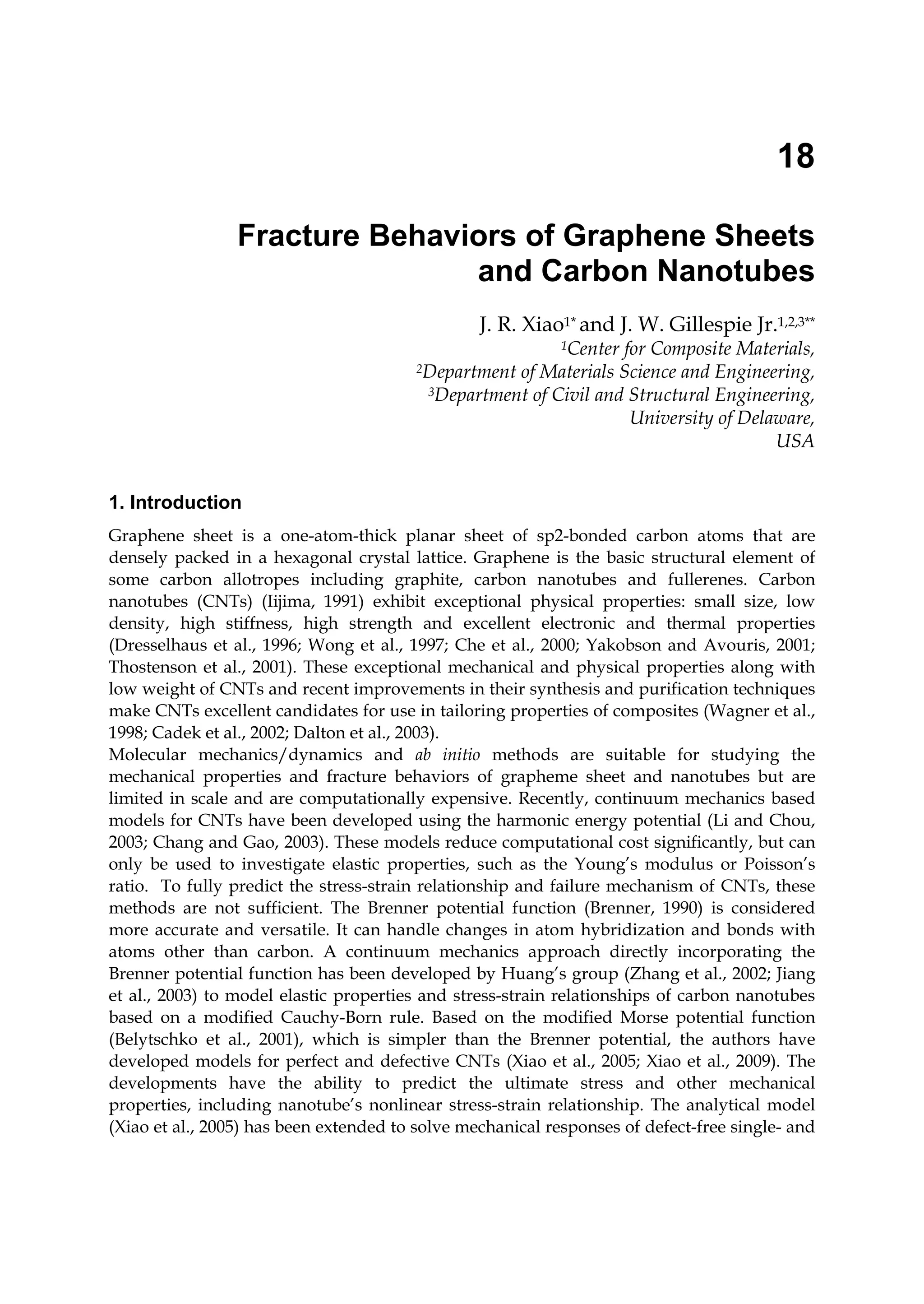
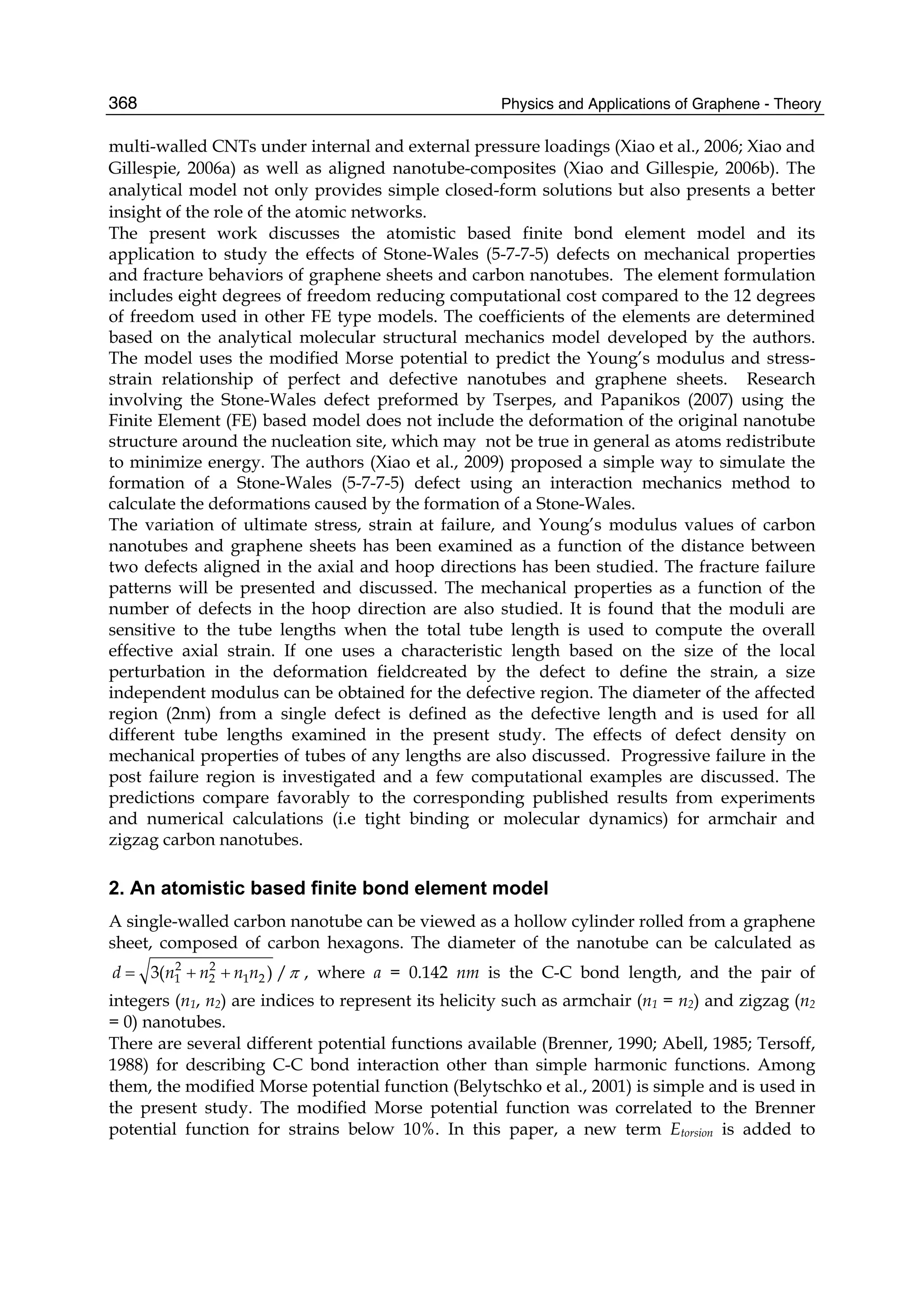
![Fracture Behaviors of Graphene Sheets and Carbon Nanotubes 369
consider the bond energy due to angle variation of bond twisting Δφ which has been found
to be negligible for defect-free tubes (Li and Chou, 2003) and was neglected in earlier studies
(Chang and Gao, 2003; Xiao et al., 2005; Xiao et al., 2006; Xiao and Gillespie, 2006a; Xiao and
Gillespie, 2006b). However, this term may play a more important role in defective tubes. The
energy potential function is given as follow:
torsionanglestretch EEEE ++= (1)
where Estretch is the bond energy due to bond stretch Δr, and Eangle is the bond energy due to
bond angle variation Δθ, and
2
)(
2
1
φφ Δ= kEtorsion
(2)
The parameters associated with the terms Estretch and Eangle can be seen in Ref (Belytschko et
al., 2001). The force constant associated with the term (2) is taken as (Li and Chou, 2003;
Cornell et al., 1995; Jorgensen and Severance, 1990) kφ = 0.278 2
/ radnmnN − .
The stretch force, the angle-variation moment and the torsional moment can be obtained
from differentiations of Eq. (1) as functions of bond stretch, bond angle variation and torsion
angle variation, respectively:
( ) rr
e eeDrF Δ−Δ−
−=Δ ββ
β 12)( (3a)
[ ]4
)(31)( θθθ θ Δ+Δ=Δ sextickkM (3b)
φφ φφ Δ=Δ kM )( (3c)
A constant bond torsional stiffness is implied by Eq. (3c). The stretch stiffness and the angle-
variation stiffness can be further obtained from differentiations of Eqs. (3a-3b) as functions
of bond stretch and bond angle variation, respectively:
( ) rr
er eeDrk ΔβΔβ
βΔ −−
−= 212)(
2
(4)
[ ]4
)(151)( θΔθΔ θθ sextickkk += (5)
Analytical solutions for predicting nonlinear mechanical behaviors of defect-free SWCNTs
have been investigated by using an effective “stick-spiral” model based on a unit cell
approach (Xiao et al., 2005). The effective “stick-spiral” model uses a stick with Eq. (3a) to
model the force-stretch relationship of the C-C bond and a spiral spring with Eq. (3b) to
model the angle bending moment resulting from an angular variation of bond angle. The
stick is assumed to have an infinite bending stiffness and finite torsional stiffness. One can
include the torsional term by using the stick with Eq. (3c).
For a defective nanotube with loss of local symmetry, the unit cell approach becomes
inappropriate, and a generalized molecular mechanics (MM) model (Sears and Batra, 2004)
or a finite element (FE) type model (Li and Chou, 2003) are needed to include the entire
molecular structure system of the defective nanotube in order to consider the effect of](https://image.slidesharecdn.com/grrphysicsandapplicationsofgraphene-theory-140422181144-phpapp02/75/physics-and_applications_of_graphene_-_theory-379-2048.jpg)
![Physics and Applications of Graphene - Theory370
defects on its mechanical response. In this paper, we propose a new FE type model for
nanotubes based on the effective “stick-spiral” model. Bond elements are developed for
simulating deformation modes of the chemical bonds.
Typically the FE type model (Li and Chou, 2003) uses a beam element (Kanchi 1993) with
sectional stretch stiffness for the force-stretch relationship of the C-C bond, sectional flexural
rigidity for the angle bending moment (Eq. 3b), and sectional torsional stiffness for the
torsional moment (Eq. 3c). Each element has 12 degrees of freedom. The major differences
between the FE type model and the effective “stick-spiral” model are the assumptions made
with respect to the bending stiffness (flexible vs rigid). The bond element used in the present
paper has infinite bending stiffness (the stick) with finite bending stiffness of the two end
joints (the spirals) indicated by the square box shown in Fig. 1. Each of the three molecular
deformation modes (stretching, angle variation, and angle torsion) are represented by
tension, bending and torsion of a bond element with 8 degrees of freedom
][ jzjyjxjiziyixie uuuuuuu φφ= . The element can be stretched (pure tension) and
torqued (pure torsion) along its axial direction and bent by relative transverse displacement
without angle changes at the two ends. The bond angle variation of the bond element can be
associated with the relative transverse displacement (e) between the two ends as dθ = e/a
(Fig. 1c). The present approach, designated the finite bond element model, is expected to
give the same solution as the “stick-spiral” model (Xiao et al., 2005; Chang and Gao, 2003)
for defect-free CNTs. The stick-spiral model with infinite bending stiffness represents the
true physical deformation modes and is able to predict both in-plane stiffness (Young’
modulus) and Poisson’s ratio of CNTs accurately.
For the bond element defined in Fig. 1 in a three-dimensional space, the elemental
equilibrium equation can be established for every bond element. The final system of
equations with appropriate boundary conditions imposed can be solved by the
displacement-control Newton-Raphson method. A MATLAB program has been written
based on finite bond element method for SWCNTs subjected to tensile loadings.
3. Validation on defect-free SWCNTs
The calculations based on our FE-based finite bond element model will be validated by
comparing with the results obtained from the analytical model (Xiao et al., 2005) for defect-
free CNTs. The initial equilibrium state of the atomistic system of a CNT is created based on
the ab initio calculations (Ye et al., 2001) where the approximate expressions of angle α and β
of armchair nanotubes are taken as 3/2πα ≈ and β = π - arcos [0.5cos(π/2n1)], respectively.
The angle α and β for zigzag nanotubes as 3/2πα ≈ and β = arcos [0.25-0.75cos(π/n1)]. The
displacement boundary conditions for the simulations are shown in Figure 2. The atoms on
the bottom edge of the tube are fixed in the axial (z) direction. One atom is fully fixed in all
three (x-, y- and z) directions to prevent rigid body rotations. The other end of the CNT was
axially displaced incrementally to introduce load into the tube.
The interatomic force per atom (f) is calculated for all atoms along the end of the nanotube
where the displacement is prescribed. For defect-free nanotubes, the force is identical for all
atoms on the end. The axial strain of the CNT is computed as ε = ΔL/L0, where L0 is the
initial length of the CNT. The force-strain relationship of nanotubes is predicted using the
procedures outlined above. Fig. 3 shows the computed force-strain relationships for](https://image.slidesharecdn.com/grrphysicsandapplicationsofgraphene-theory-140422181144-phpapp02/75/physics-and_applications_of_graphene_-_theory-380-2048.jpg)
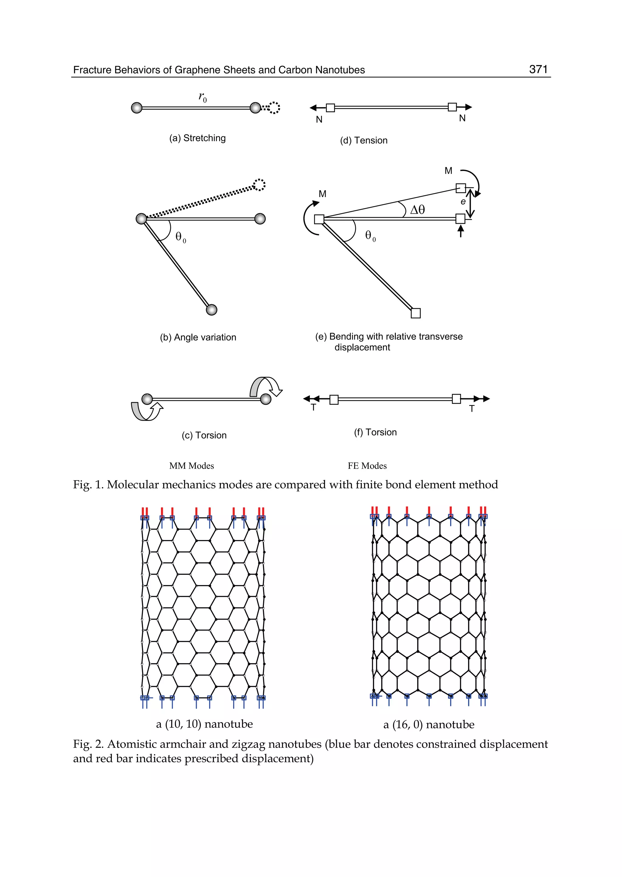
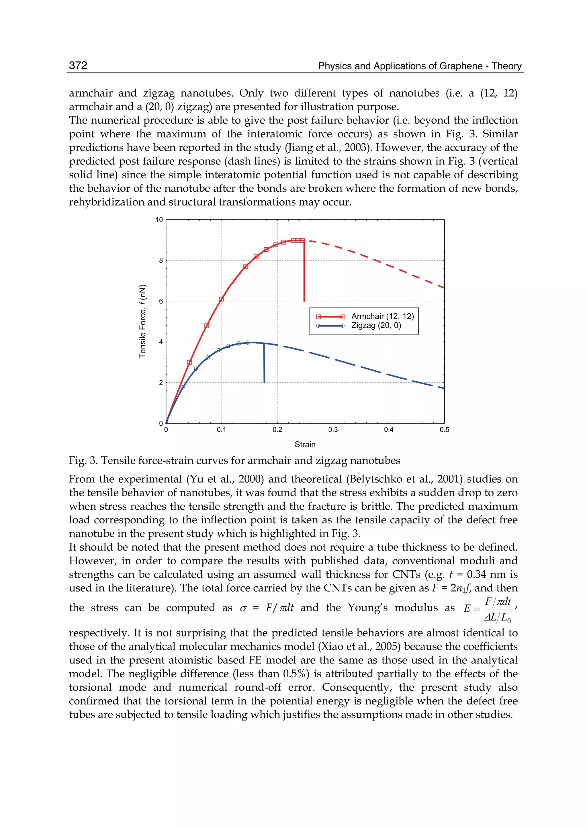
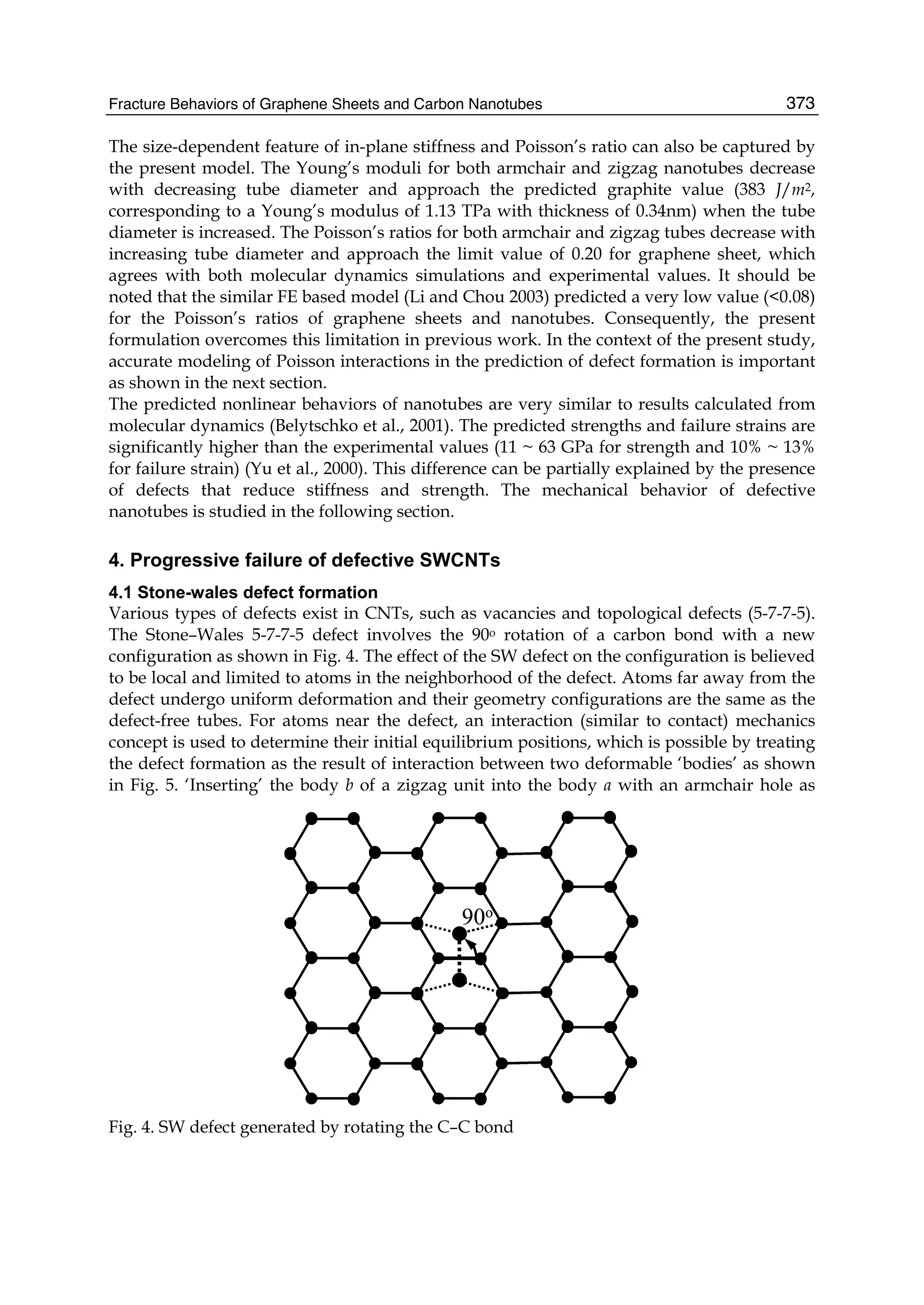
![Physics and Applications of Graphene - Theory374
defined in Fig. 5 and forcing them to be coincident at four specific locations will cause re-
configuration of the system within a localized region because of the geometrical distortions
that exist at the four locations. Assuming the same in-plane properties for each body
(governed by the same potential function), self-equilibrating ‘residual’ or internal forces will
be generated between disturbed atoms if we assume that there is no net atomic force
between atoms at equilibrium state of defect-free region (reference state). The resulting
configuration corresponds to the minimized energy state of a defective graphene sheet and
CNT.
The finite bond element method is used for describing atomistic force-displacement
interaction for both bodies to study how the two regions conform to each other. The two
deformable bodies Ωe (e = a, b) are shown in Fig. 5. The interaction sites (contact ‘surface’)
consists of four atoms (1, 2, 3 and 4) that exist in both bodies with prescribed displacements
along e
uΓ and tractions applied on e
tΓ (e = a, b). If the initial gap along the interaction
surface of the two bodies is denoted by g (= (uxi uyi uzi), i = 1,2,3,4) the interaction condition
can be described in the form of inequalities as:
Fc ≤ 0 g ≥ 0 (8a)
g Fc = 0 (8b)
where Fc )( ziyixi FFF is the interaction force vector of the four interfacial atoms. For each
body, displacement and force fields are determined by the molecular mechanics and can be
written in the following condensed matrix form:
⎭
⎬
⎫
⎩
⎨
⎧ −
=
⎭
⎬
⎫
⎩
⎨
⎧
⎥
⎦
⎤
⎢
⎣
⎡
c
ct
b
a
b
a
F
FF
u
u
K
K
0
0 (9)
in which ua and ub are components of the displacement vector (same size as the gap vector g)
of the four atoms in the body a and b, respectively. Ft is the applied external force vector. Ka
is the condensed stiffness matrix of the body a with the displacements ua as the basic
unknowns and contents of stiffness contributions from all elements of the body a. Kb is the
condensed stiffness matrix of the body b. By introducing the following transformation:
⎭
⎬
⎫
⎩
⎨
⎧
⎥
⎦
⎤
⎢
⎣
⎡
=
⎭
⎬
⎫
⎩
⎨
⎧
g
u
I
II
u
u a
b
a
0
(10)
where [I] is the identity matrix. Eq. (9) can be easily transformed to:
cFFKg += (11)
in which
[ ] abaaa KKKKKK 1−
+−= (12a)
[ ] tbaat FKKKFF 1−
+−= (12b)
So that the force Fc, which is required to close the gap to achieve coincident atom locations,
can be calculated from Eq. (11) for the initial ( 0=F ) and/or loaded states as:](https://image.slidesharecdn.com/grrphysicsandapplicationsofgraphene-theory-140422181144-phpapp02/75/physics-and_applications_of_graphene_-_theory-384-2048.jpg)
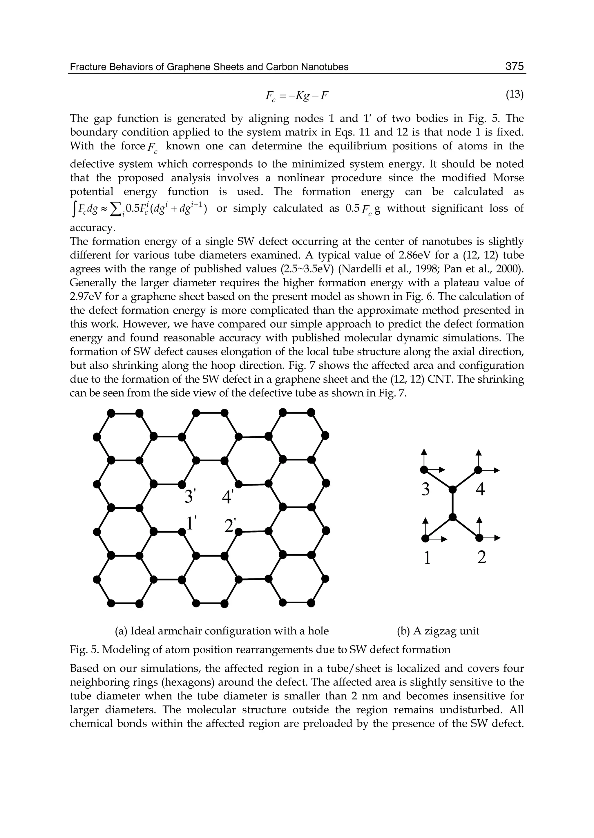
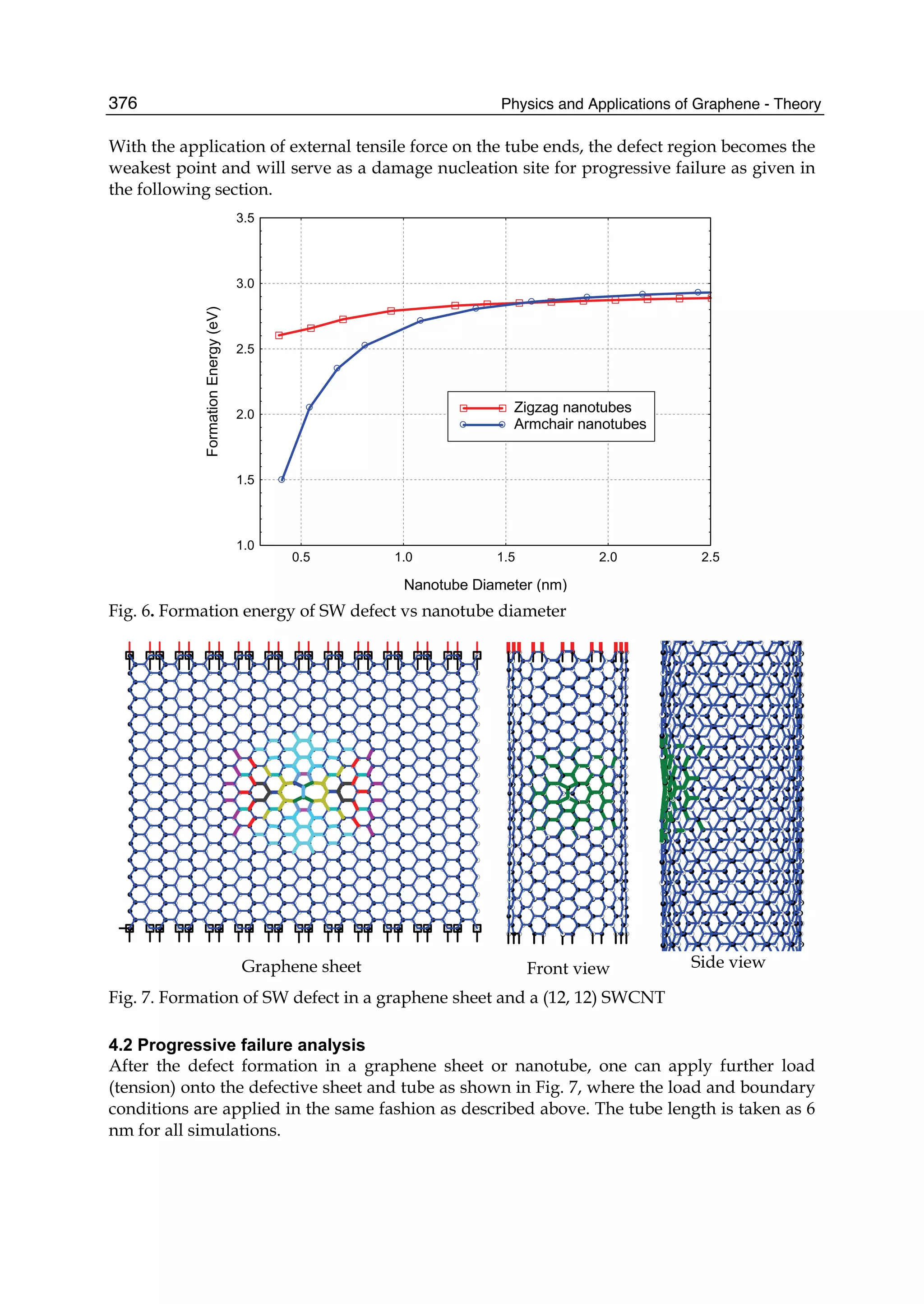
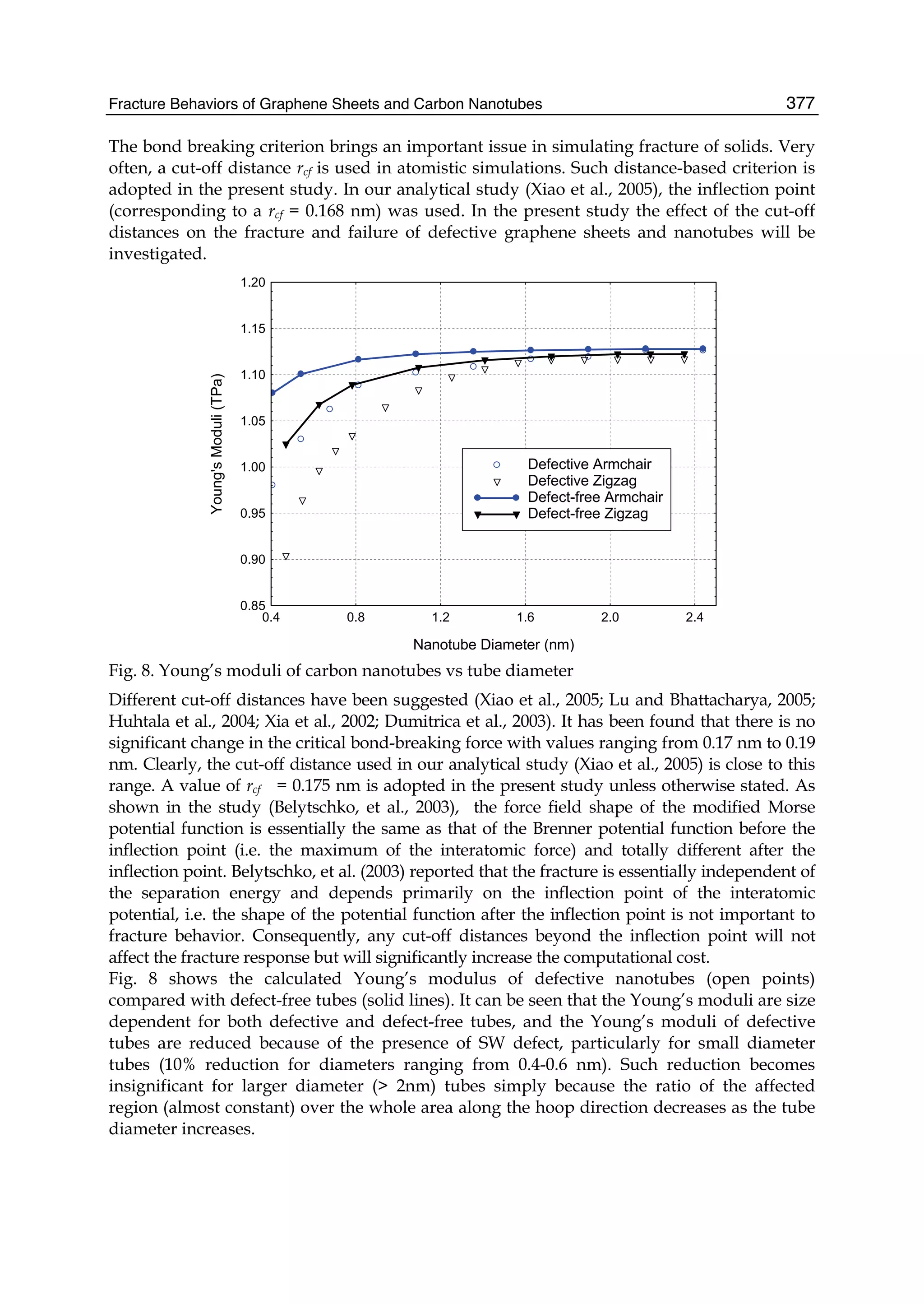
![Fracture Behaviors of Graphene Sheets and Carbon Nanotubes 381
deformations of the tube are taken into account for the next defect. The defects are therefore
created at specific locations sequentially, not simultaneously. The effect of randomly
distributed multiple defects on mechanical properties of nanotubes has been studied by Lu
and Bhattacharya [17] using MD. Predictions on mechanical properties of CNTs with
multiple defects based on continuum mechanics based models have not been well studied.
The present study provides understanding of the effects of multiple defects on the Young’s
modulus, ultimate strength, and strain at failure of the defective CNTs. After defect
formations in a graphene sheet or nanotube, one can apply further load (tension) onto the
defective sheet and tube as shown in Fig. 11, where the load and boundary conditions are
applied in the same fashion as described above. Different tube lengths are examined.
(a) Graphene sheet
(b) CNT
Fig. 11. Fracture pattern of a graphene sheet and tube with two defects along its axial
direction
4.3.1 Effects on young’s modulus
From our simulations, it has been found that graphene sheets and CNTs with multiple
defects along its axial direction (with separation distance larger than 2nm) show similar
moduli and strengths as those with single defect, because the determining factor is the
weakest cross-section. It should be noted that there is no defect interactions when the
separation distance is greater than 2nm. The present study focuses on the effects of two](https://image.slidesharecdn.com/grrphysicsandapplicationsofgraphene-theory-140422181144-phpapp02/75/physics-and_applications_of_graphene_-_theory-391-2048.jpg)
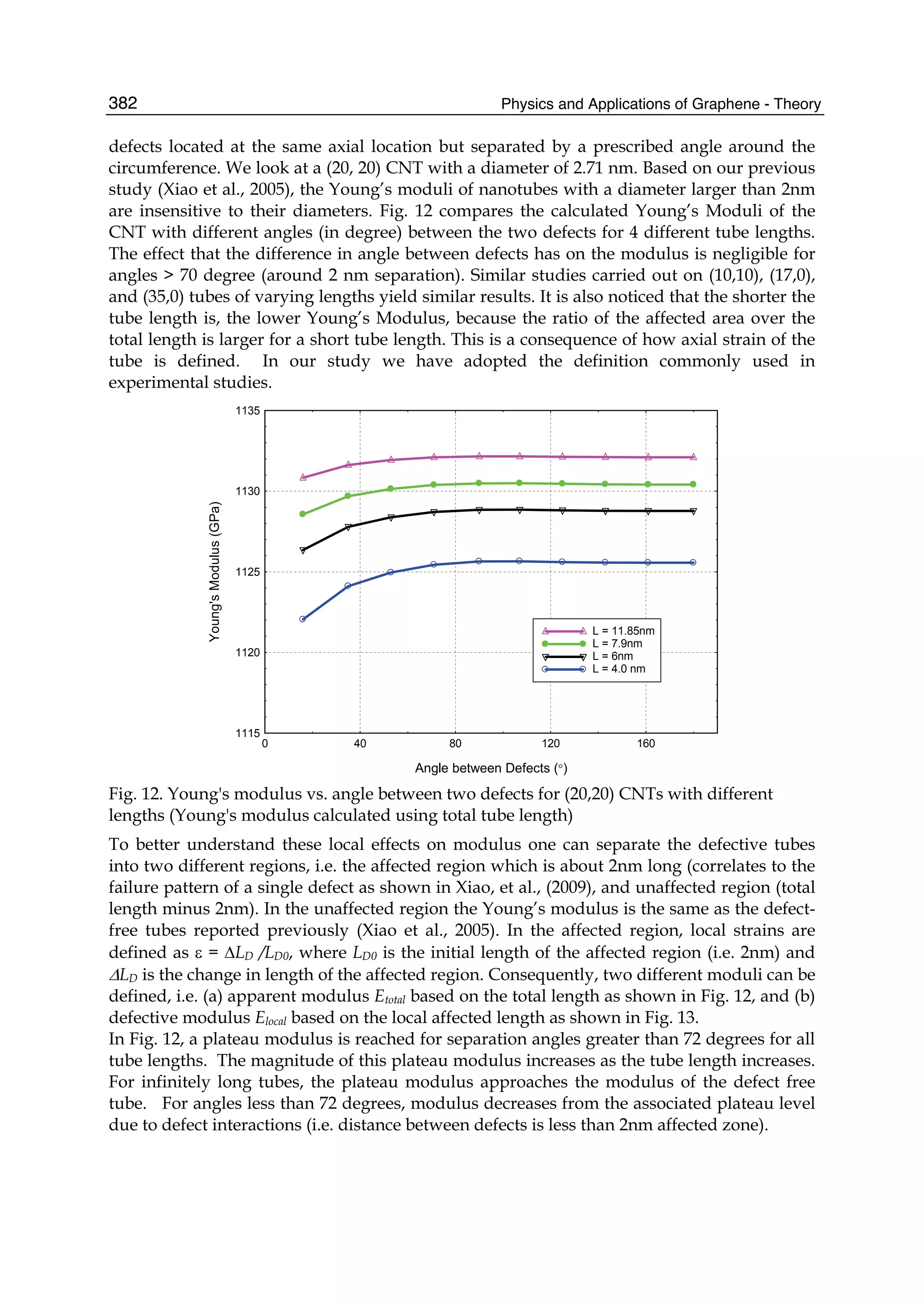
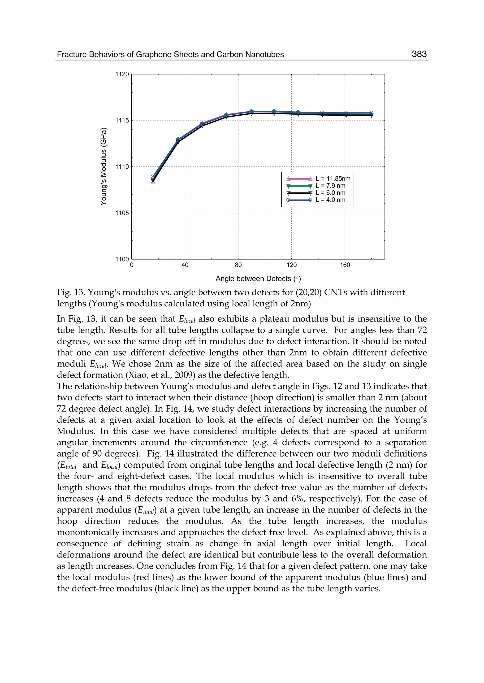
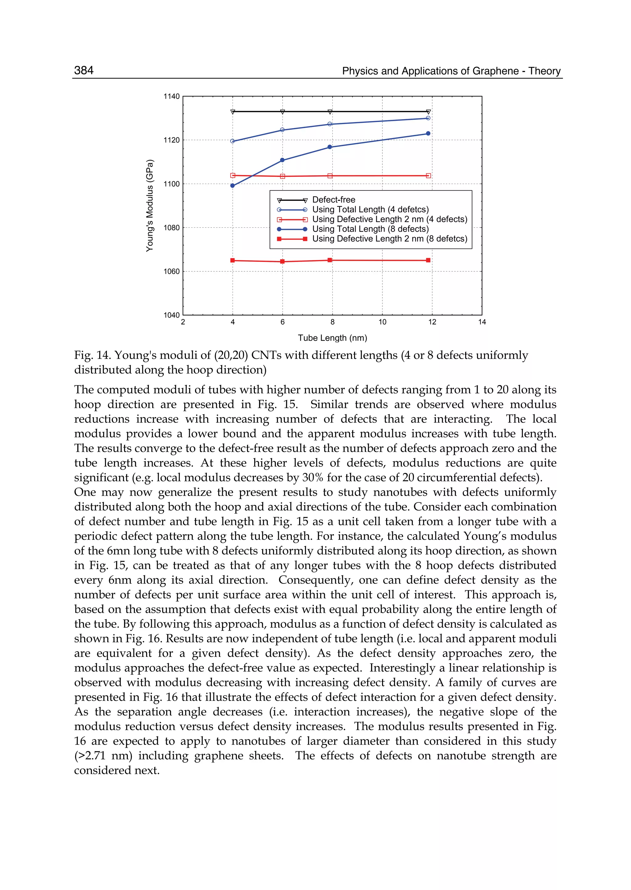
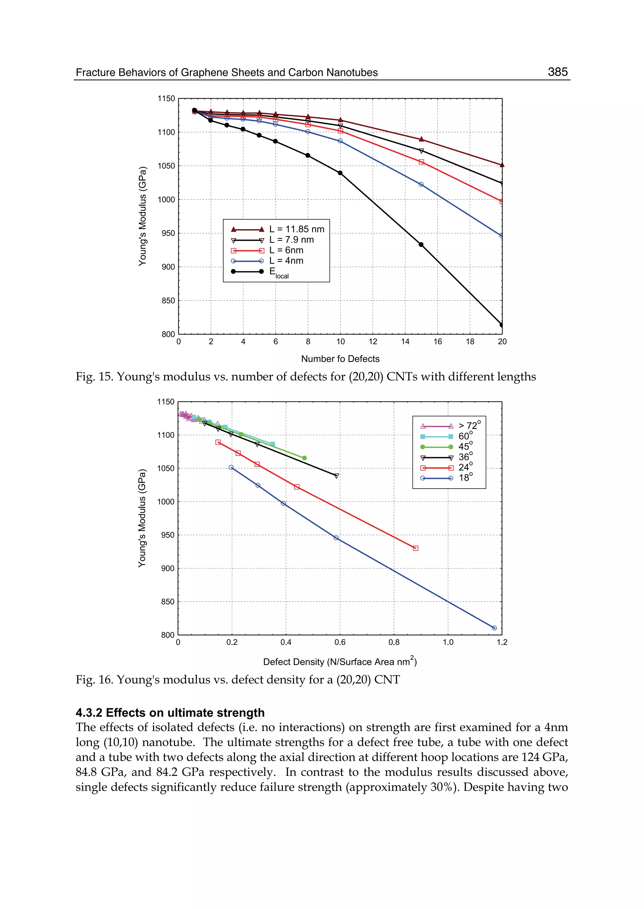
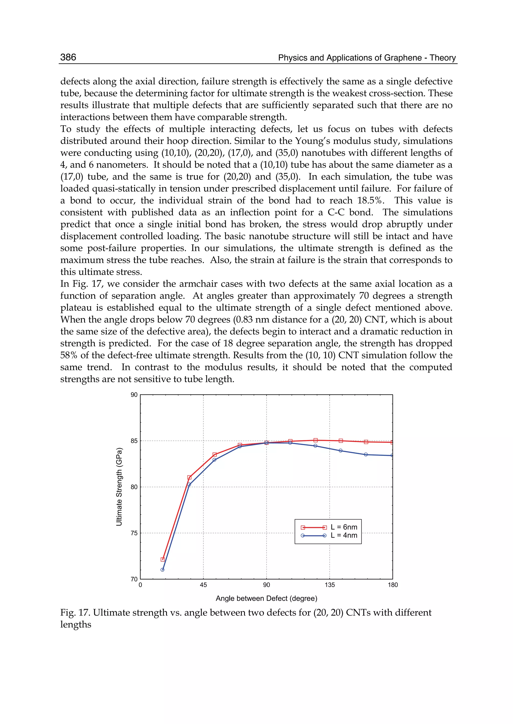
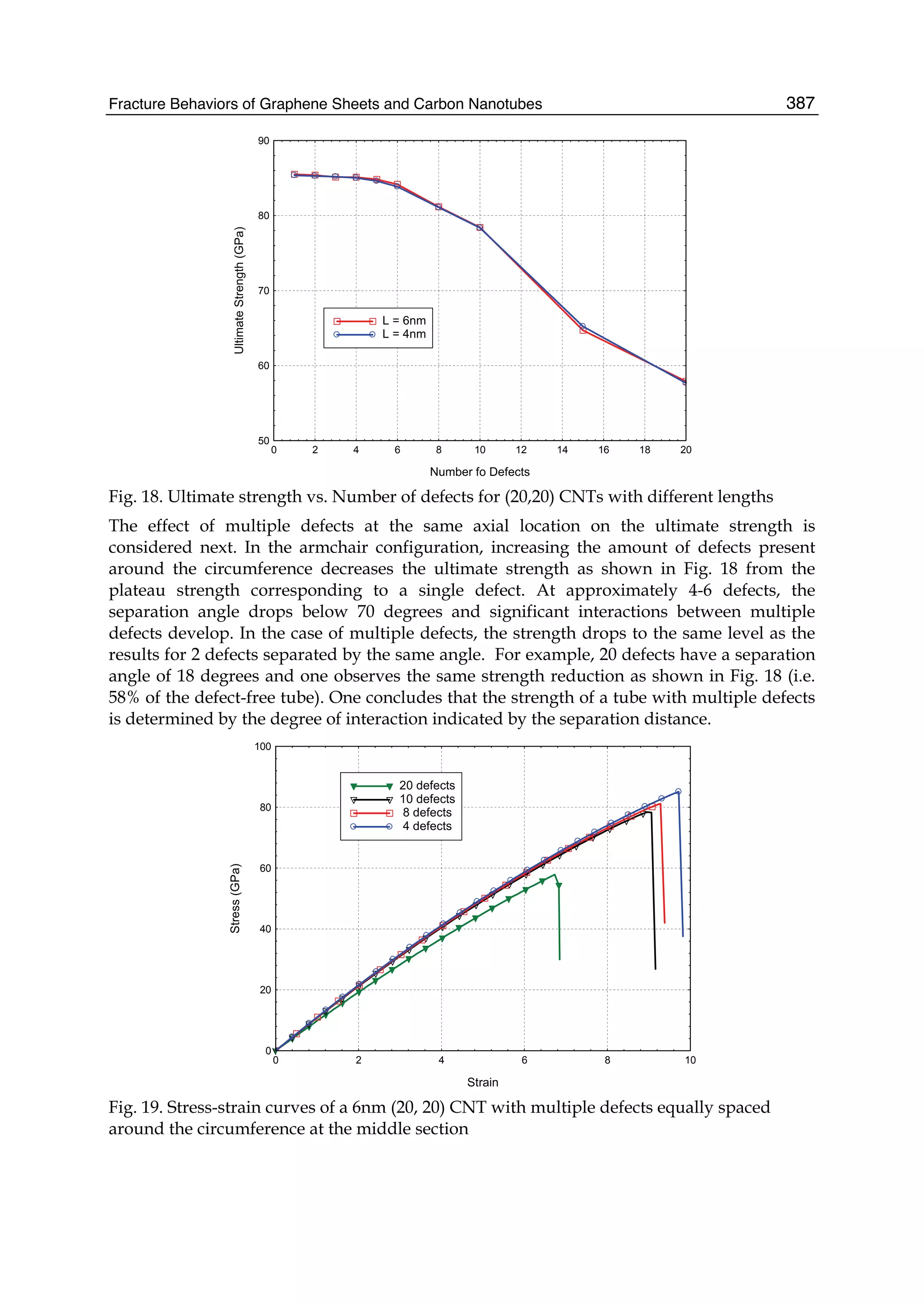
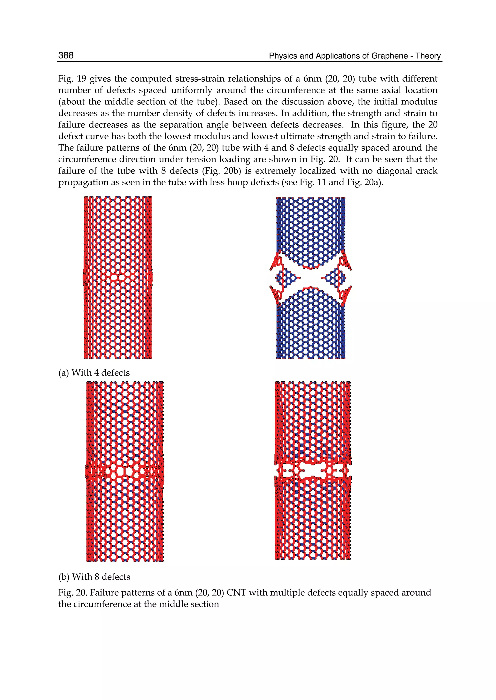


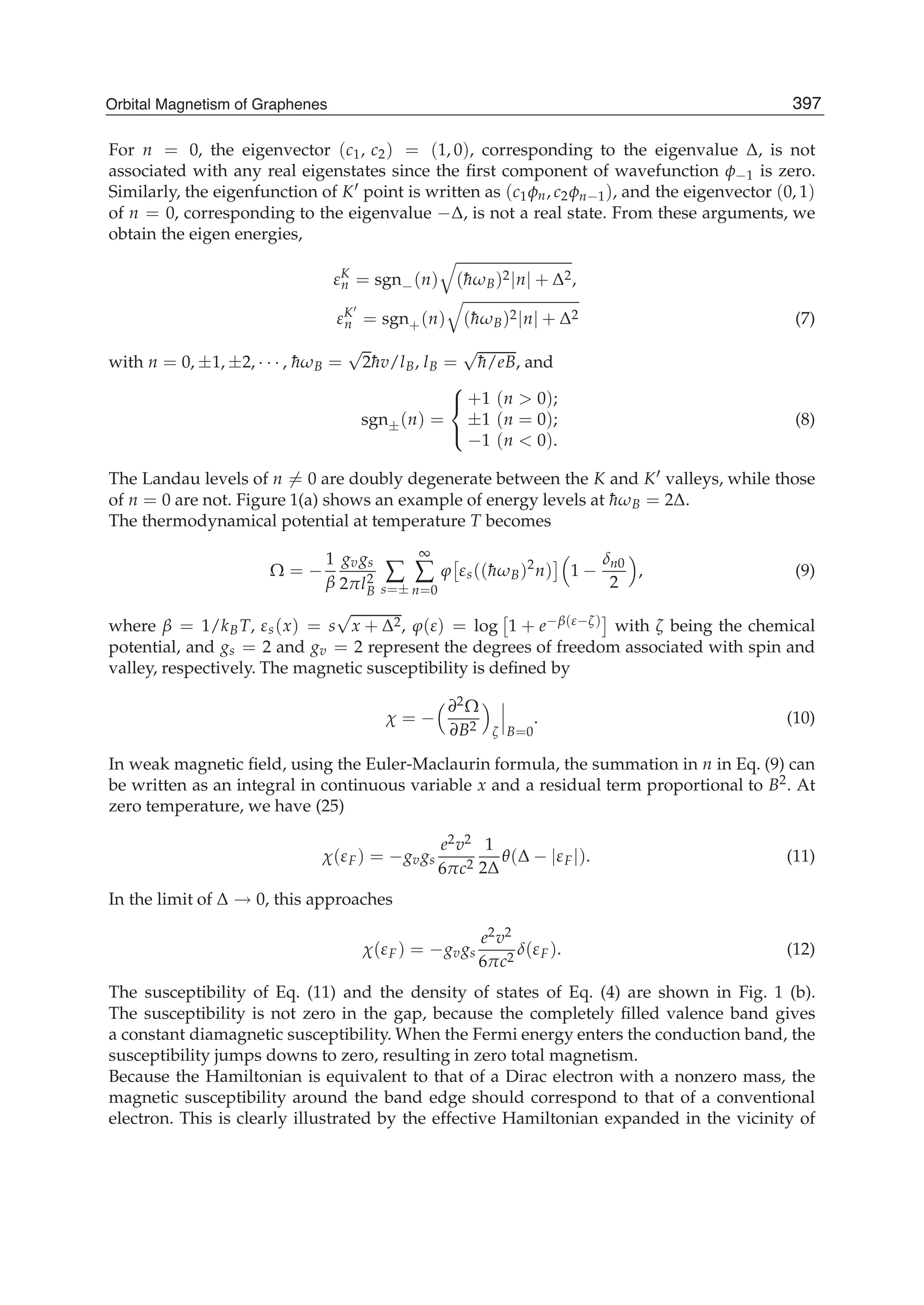
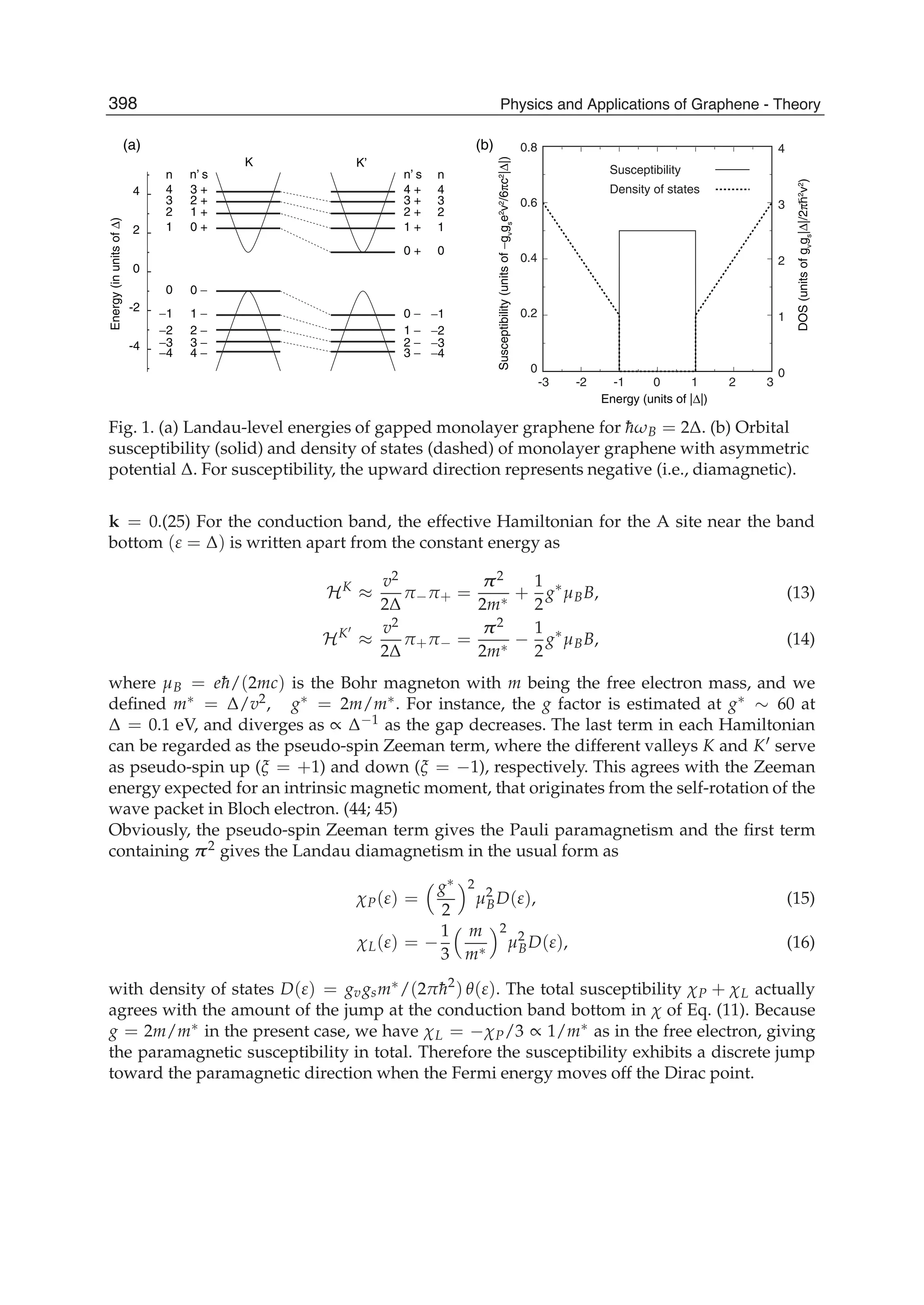
![In the original Hamiltonian, the Landau-level energies in Eq. (7) can be rewritten as
εξ,s,n = s (¯hωB)2 n +
1
2
+
ξs
2
+ Δ2
(n = 0, 1, 2, · · · ). (17)
Figure 1(a) shows energy levels for ¯hωB = 2Δ and the relationship between the different
labeling schemes of Eqs. (7) and (17). For the conduction band, the levels of the same n with
opposite pseudo-spins ξ = ±1 share the same Landau level function labeled by n on the A
site, on which the states near the conduction-band bottom (ε = Δ) have most of the amplitude.
For the valence band, similarly, n describes the index of the Landau-level function at the B
site.
2.2 Response to non-uniform magnetic field
We extend the argument to spatially modulated magnetic fields. The graphene in a
non-uniform magnetic field was studied in the context of the electron confinement, (46–48)
the peculiar band structures in superlattice, (49; 50) transport,(51) and the quantum Hall
effect.(52; 53) In the following, we introduce a linear response theory to general field
distributions. (24) We consider an isotropic 2D system, under a magnetic field given by
B(r) = [∇ × A(r)]z with vector potential A(r). Here r = (x, y) denotes 2D position on the
graphene. We define j(r) = (jx, jy) as the 2D electric current density induced in the system.
Within the linear response, the Fourier-transforms of j(r) and A(r) satisfy
jμ(q) = ∑
ν
Kμν(q)Aν(q), (18)
with response function Kμν. The gauge invariance for A requires ∑ν Kμν(q) qν = 0, and the
continuous equation, ∇ · j(r) = 0, imposes another constraint ∑μ qμ Kμν(q) = 0. To meet both
requirements, tensor Kμν needs to be in the form,
Kμν(q) = K(q) δμν −
qμqν
q2
. (19)
On the other hand, because ∇ · j(r) = 0, we can express j(r) as jx = c ∂m/∂y, jy = −c ∂m/∂x,
with m(r) being the local magnetic moment perpendicular to the layer. In the linear response,
its Fourier transform is written as
m(q) = χ(q)B(q), (20)
with the magnetic susceptibility χ(q). Equations (18) and (20) are complementary, and both
response functions χ(q) and K(q) are related by
χ(q) =
1
cq2
K(q). (21)
We apply the above formulation to graphene without gap, i.e., Δ = 0. The eigenstates at zero
magnetic field are labeled by (s, k) with s = +1 and −1 being the conduction and valence
bands, respectively, and wave vector k. The eigen energy is given by εsk = s¯hvk, and the
corresponding wavefunction is ψsk(r) = eik·r Fsk/
√
S with Fsk =
1
√
2
eiθ
s
, where k and θ
are defined by (kx, ky) = k(cos θ, sin θ) and S is the system area.
399Orbital Magnetism of Graphenes](https://image.slidesharecdn.com/grrphysicsandapplicationsofgraphene-theory-140422181144-phpapp02/75/physics-and_applications_of_graphene_-_theory-409-2048.jpg)
![0 1 2 3 4 5
0
0.2
0.4
0.6
0.8
1
-1 -0.5 0 0.5 1
0
0.5
1
1.5
−χ[unitsofgv
gs
e2
v/(16πhc2
2kF
)]
q/(2kF
)
(a) (b)
−χ[unitsofgv
gs
e2
v/(16πhc2
q)]
εF
/ hvq
Fig. 2. Magnetic susceptibility χ(q ; εF) in graphene plotted against (a) q with fixed εF, and (b)
εF with fixed q. Dotted line in (a) represents the undoped case, Eq. (24).
The local current density at r0 is calculated as the expectation value of current-density operator
ˆj(r0) = ev σ δ(r − r0) over the occupied states. In the first order perturbation in A, we have
Kμν(q) = −
gvgse2
c
1
S ∑
ss k
f (εsk) − f (εs k+q)
εsk − εs k+q
(F†
sk vν Fs k+q) (F†
s k+q vμ Fsk), (22)
where vμ = vσμ.
At the zero temperature, this can be explicitly calculated as
χ(q ; εF) = −
gvgse2v
16¯hc2
1
q
θ(q − 2kF) 1 +
2
π
2kF
q
1 −
2kF
q
2
−
2
π
sin−1 2kF
q
, (23)
where kF = |εF|/(¯hv) is the Fermi wave number. Significantly, χ vanishes in range q < 2kF,
i.e., no current is induced when the external field is smooth enough compared to the Fermi
wavelength. At εF = 0, particularly, we have
χ(q; 0) = −
gvgse2v
16¯hc2
1
q
. (24)
We plot χ(q ; εF) against (a) q and (b) εF in Fig. 2. As a function of q, the susceptibility suddenly
starts from zero at q = 2kF, and rapidly approaches the universal curve (24). As a function of
εF with fixed q, it is nonzero only in a finite region satisfying |εF| < ¯hvq/2, and its integral
over εF becomes constant −gvgse2v2/(6πc2). Thus, in the limit of q → 0 it goes to the previous
result Eq. (12). The susceptibility of the carbon nanotube to a uniform field perpendicular
to the axis has the equivalent expression of Eq. (24) where q is replaced by 2π/L with tube
circumference L. (54; 55)
The undoped graphene (εF = 0) has a special property in which the counter magnetic field
induced by the response current has a spacial distribution similar to that of external magnetic
field, regardless of its length scale (24). Let us assume that a sinusoidal external field B(r) =
B cos qx is applied to undoped graphene. With the susceptibility Eq. (24), the response current
is calculated as jy(r) = −[gvgse2vB/(16¯hc)] sin qx. The current induces a counter magnetic
field which reduces the original field. The z component of the induced field on graphene
becomes
Bind(r) = −αgB(r), αg =
2πgvgse2v
16¯hc2
≈ 4×10⁻⁵
. (25)
400 Physics and Applications of Graphene - Theory](https://image.slidesharecdn.com/grrphysicsandapplicationsofgraphene-theory-140422181144-phpapp02/75/physics-and_applications_of_graphene_-_theory-410-2048.jpg)
![Because the ratio is independent of q, Eq. (25) is actually valid for any external field B(r), i.e.,
the magnetic field on the graphene is always reduced by the same factor 1 − αg. This property
holds whenever χ(q) is written as C/q with constant C.
The argument of the magnetic field screening can be extended in the three dimensional field
distribution. Let us suppose a situation when a certain magnetic object is placed above the
undoped graphene (z > 0), which produces an external magnetic field B(ρ) in 3D space
ρ = (x, y, z). Then, the followings are concluded: (i) On the other side of the graphene (z < 0),
the induced field becomes −αgB(ρ), i.e., the external field is screened by the factor 1 − αg. (ii)
On the same side (z > 0), the induced field is given by αgRz[B(x, y, −z)], where Rz is the
vector inversion with respect to z = 0. Namely, this is equivalent to a field of the mirror image
of the original object reflected with respect to z = 0, and reduced by αg.
Using the property of magnetic mirroring, we can easily estimate the magnetic repulsive
force which works between undoped graphene and magnetic objects. If we put on the top
of graphene the permanent magnet with surface magnetic flux σm, the repulsive force per unit
area is given by 2παgσ2
m, which is a force between a sheet with magnetic monopole density σm
and its mirror image with αgσm. At σm which amounts to the surface flux 1T (e.g., neodymium
magnet),(56) this is as large as 0.16 gram weight /cm2, which is surprisingly large as a force
generated by a thin film only one atom thick.
The 1/q dependence of χ(q), which is responsible for peculiar diamagnetic responses argued
above, is a characteristic property common to general k-linear Hamiltonian. This can be shown
using the scaling argument as follows. We consider an isotropic two-dimensional system, in
which Hamiltonian H contains only terms linear in πx and πy. The velocity operator vμ =
∂H/∂πμ is then a constant matrix independent of π. Similarly to graphene, the eigen energy
and the wavefunction are written as εn,k and ψn,k(r) = eik·r Fn,k/
√
S, respectively, with the
subband index n and the wavenumber k. The response function Kμν(q) can then be written
in the same form as Eq. (22), with index s replaced with n.
If we change the energy and wave number scales by an arbitrary factor α as
ε = α˜ε, ki = α˜ki, (26)
then the Hamiltonian becomes formally identical under that transformation, since the
coefficients of k-linear terms in the Hamiltonian remain unchanged. The eigen energy and
eigen function obey εn, ˜k = εn,k/α and Fn, ˜k = Fn,k. Using them, we can show that the response
function Kμν(q) scales at zero temperature and at zero Fermi energy as
Kμν
q
α
=
Kμν(q)
α
, (27)
which allows us to write as K(q) = Cq with certain number C. With Eq. (21), the susceptibility
χ becomes
χ(q) =
C
cq
. (28)
Similar scaling argument also applies to χ(εF) at q = 0, leading to χ(εF) ∝ δ(εF) in any
k-linear Hamiltonian.(26)
3. Bilayer graphene
Bilayer graphene is a pair of graphene layers arranged in AB (Bernal) stacking and includes A1
and B1 atoms on layer 1 and A2 and B2 on layer 2.(33–41) The schematics of the AB stacked
401Orbital Magnetism of Graphenes](https://image.slidesharecdn.com/grrphysicsandapplicationsofgraphene-theory-140422181144-phpapp02/75/physics-and_applications_of_graphene_-_theory-411-2048.jpg)
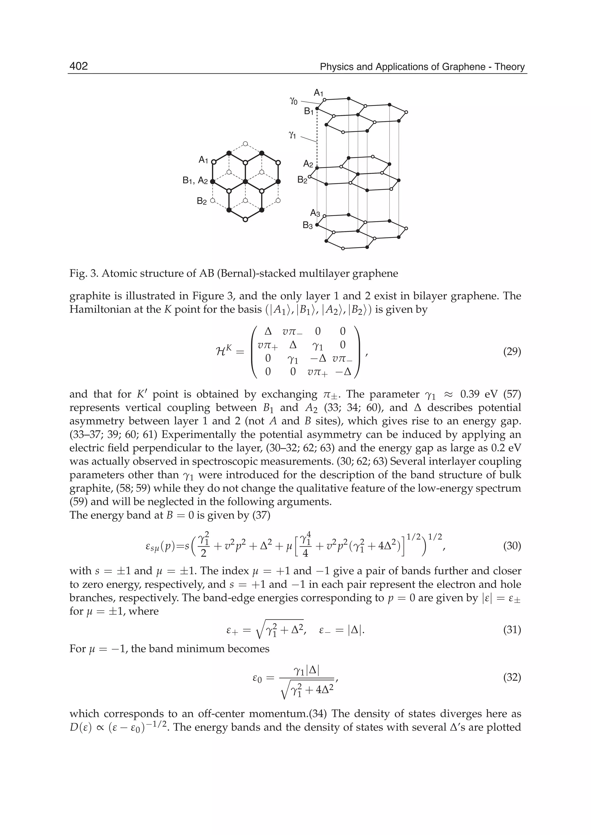
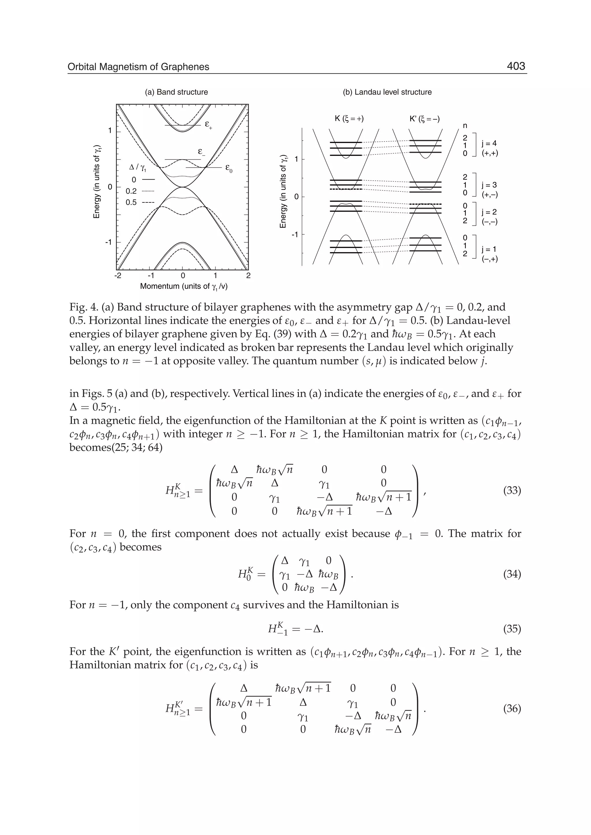
![For n = 0, the matrix for (c1, c2, c3) becomes
HK
0 =
⎛
⎝
Δ ¯hωB 0
¯hωB Δ γ1
0 γ1 −Δ
⎞
⎠ , (37)
and for n = −1, that for c1 is
HK
−1 = Δ. (38)
If we extend the definition of the matrix of Eq. (33) to n = 0, its three eigenvalues agree with
those of HK
0 and the rest with that of HK
−1. Similarly, the matrix of Eq. (36) with n = 0 gives
eigenvalues of HK
0 and HK
−1. Thus we can use Eqs. (33) and (36) with n ≥ 0 to produce the
full spectrum. By introducing the pseudo-spin variable ξ = ±1, the Hamiltonian is combined
into a single expression,
H
ξ
n =
⎛
⎜
⎜
⎝
Δ
√
xn− 0 0
√
xn− Δ γ1 0
0 γ1 −Δ
√
xn+
0 0
√
xn+ −Δ
⎞
⎟
⎟
⎠ , (39)
with
xn± = xn ±
1
2
ξδ, (40)
and
xn = n +
1
2
δ, δ = (¯hωB)2
. (41)
We write the eigenvalues of H
ξ
n as
εj(xn, ξδ) (j = 1, 2, 3, 4), (42)
in the ascending order in energy (j = 1 and 2 for valence bands and j = 3 and 4 for
the conduction bands). The second argument in εj(xn, ξδ) represents the dependence on B
which are not included in xn. Figure 4 shows the example of the Landau-level spectrum at
Δ/γ1 = 0.2 and ¯hωB/γ1 = 0.5, where the thick dashed lines represent the Landau level which
originally belongs to n = −1 at opposite valleys. The correspondence between quantum
numbers j and (s, μ) are indicated in the figure.
The thermodynamic potential becomes
Ω = −
1
β
gs
2πl2
B
∑
ξ,j
∞
∑
n=0
ϕ εj(xn, ξδ)
= −
1
β
gs
4π¯h2
v2 ∑
ξ,j
∞
0
ϕ εj(x, ξδ) dx +
δ2
24
∂ϕ[εj(x, 0)]
∂x x=0
+ O(δ3
), (43)
where we used the Euler-Maclaurin formula in the second equation. The first term in the
bracket can be transformed by changing the integral variable from x to ε as
1
β
∞
0
ϕ εj(x, ξδ) dx =
∞
−∞
f (ε) nj(ε, ξδ)dε, (44)
404 Physics and Applications of Graphene - Theory](https://image.slidesharecdn.com/grrphysicsandapplicationsofgraphene-theory-140422181144-phpapp02/75/physics-and_applications_of_graphene_-_theory-414-2048.jpg)
![-0.5
0
0.5
1
-1.5 -1 -0.5 0 0.5 1 1.5
0
2
4
6
8
(a) DOS (b) Susceptibility
Δ / γ1
0.2
0.5
0
Δ / γ1
0.2
0.5
0
DOS(unitsofgv
gs
γ1
/4πh2
v2
)
Susceptibility(unitsof−gv
gs
e2
v2
/πc2
γ1
)
Energy (units of γ1
)
-1.5 -1 -0.5 0 0.5 1 1.5
Energy (units of γ1
)
ε+
ε−
ε0
ε+
ε−
ε0
Fig. 5. (a) Density of states, and (b) magnetic susceptibility of bilayer graphenes with the
asymmetry gap Δ/γ1 = 0, 0.2, and 0.5. Arrows indicate the energies of ε0, ε− and ε+ for
Δ/γ1 = 0.5. In (b), upward direction represents negative (i.e., diamagnetic) susceptibility.
In the energy region −ε− < ε < −ε0 near the top of the valence band, both x+ and x− are
real and positive, giving the states at outer and inner equi-energy circle of the band j = 2,
respectively. Then we have
n
(2)
2 (ε) =
∂2
∂δ2
(−x+ + x−)
δ=0
=
γ2
1(Δ2 − ε2)
2[(4Δ2 + γ2
1)(ε2 − ε2
0)]3/2
. (52)
When the energy approaches to −ε0 from the negative side, the integral of n
(2)
2 (ε), thus the
susceptibility, diverges in positive direction as ∝ (ε + ε0)−1/2 in the same manner as the
density of states. The same divergence occurs at the bottom of the conduction band, +ε0,
because of the electron-hole symmetry.
In the vicinity of the bottom of the excited conduction band, ε = ε+, we have
n
(2)
4 (ε) =
∂2
∂δ2
x−θ(x−)
δ=0
=
∂2x−
∂δ2
θ(x−) +
∂x−
∂δ
2
δ(x−)
δ=0
, (53)
where we used x−δ(x−) = 0 and x−δ (x−) = −δ(x−). Using Eq. (48), we find that the
susceptibility makes a discrete jump at ε+ as
χ(ε+ + 0) − χ(ε+ − 0) = gvgs
e2v2
πc2
Δ2 Δ2 + γ2
1
γ2
1(2Δ2 + γ2
1)
−
2Δ2 + γ2
1
12γ2
1 Δ2 + γ2
1
, (54)
where the first term in the bracket comes from the integral of the delta function in Eq. (53) and
the second term from the step function in Eq. (48).
Near ε+, the eigenstates are given primarily by the dimer states composed of |B1 and |A2 .
The effective Hamiltonian is described by the second order in interband interaction with the
conduction-band bottom |A1 and the valence-band top |B2 , where each process gives a term
∝ π+π− or ∝ π−π+. In symmetric bilayer with Δ = 0, the terms π+π− and π−π+ have the
same coefficient and the pseudo-spin Zeeman term identically vanishes. When Δ becomes
nonzero, the two coefficients shift from each other linearly in Δ because of the band-gap
406 Physics and Applications of Graphene - Theory](https://image.slidesharecdn.com/grrphysicsandapplicationsofgraphene-theory-140422181144-phpapp02/75/physics-and_applications_of_graphene_-_theory-416-2048.jpg)
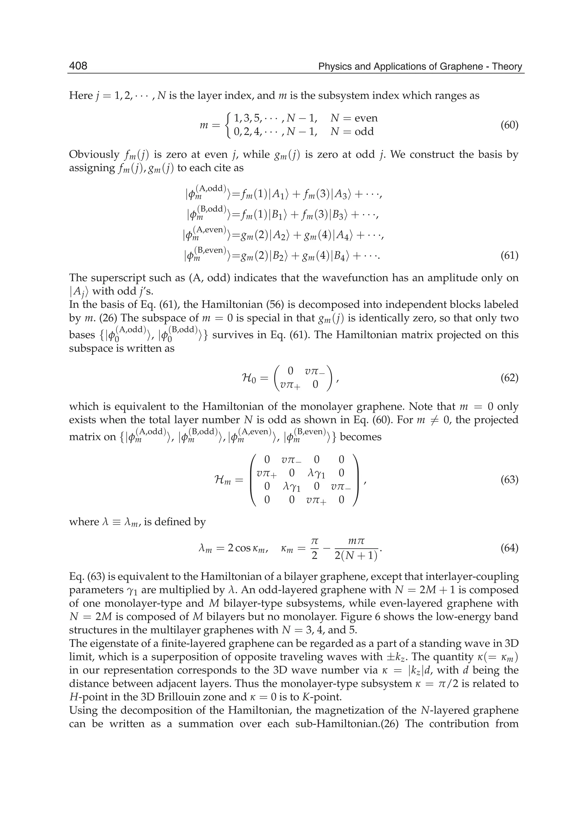
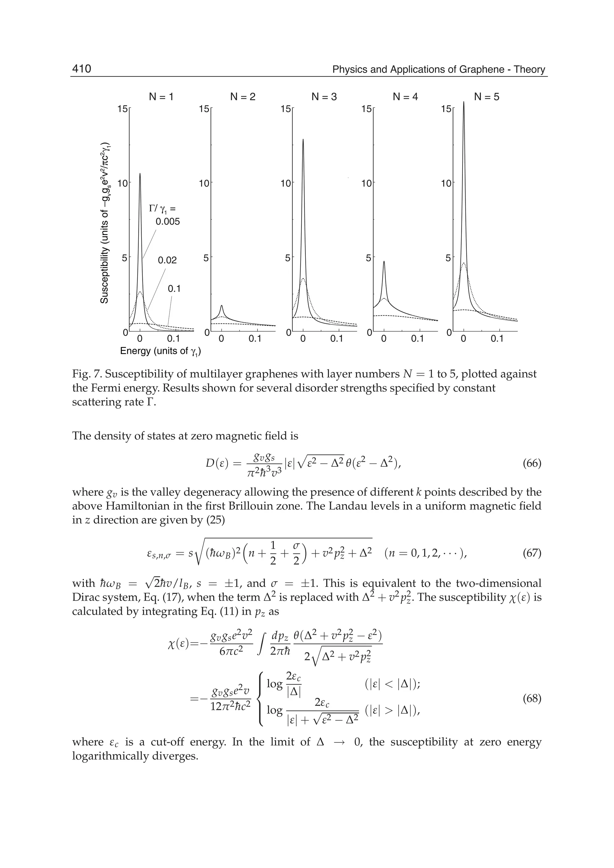
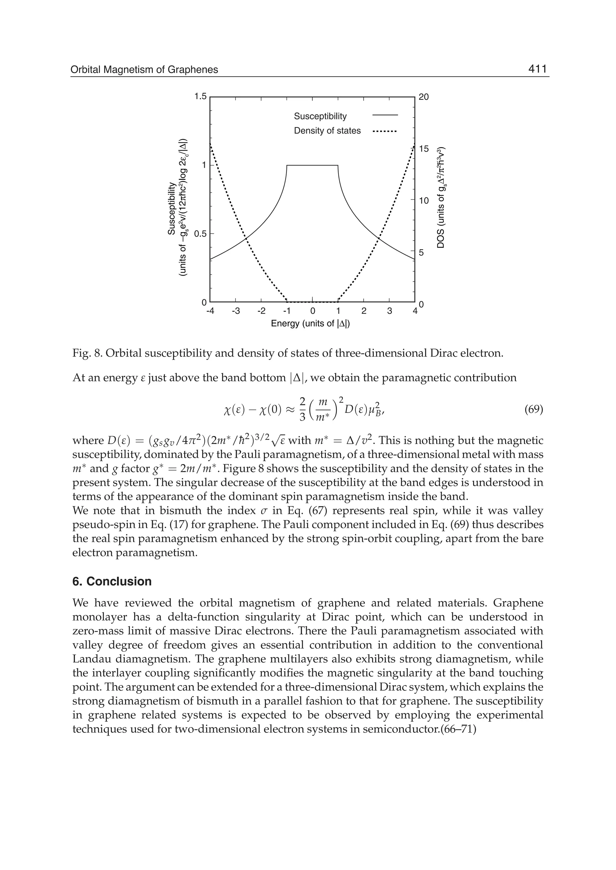


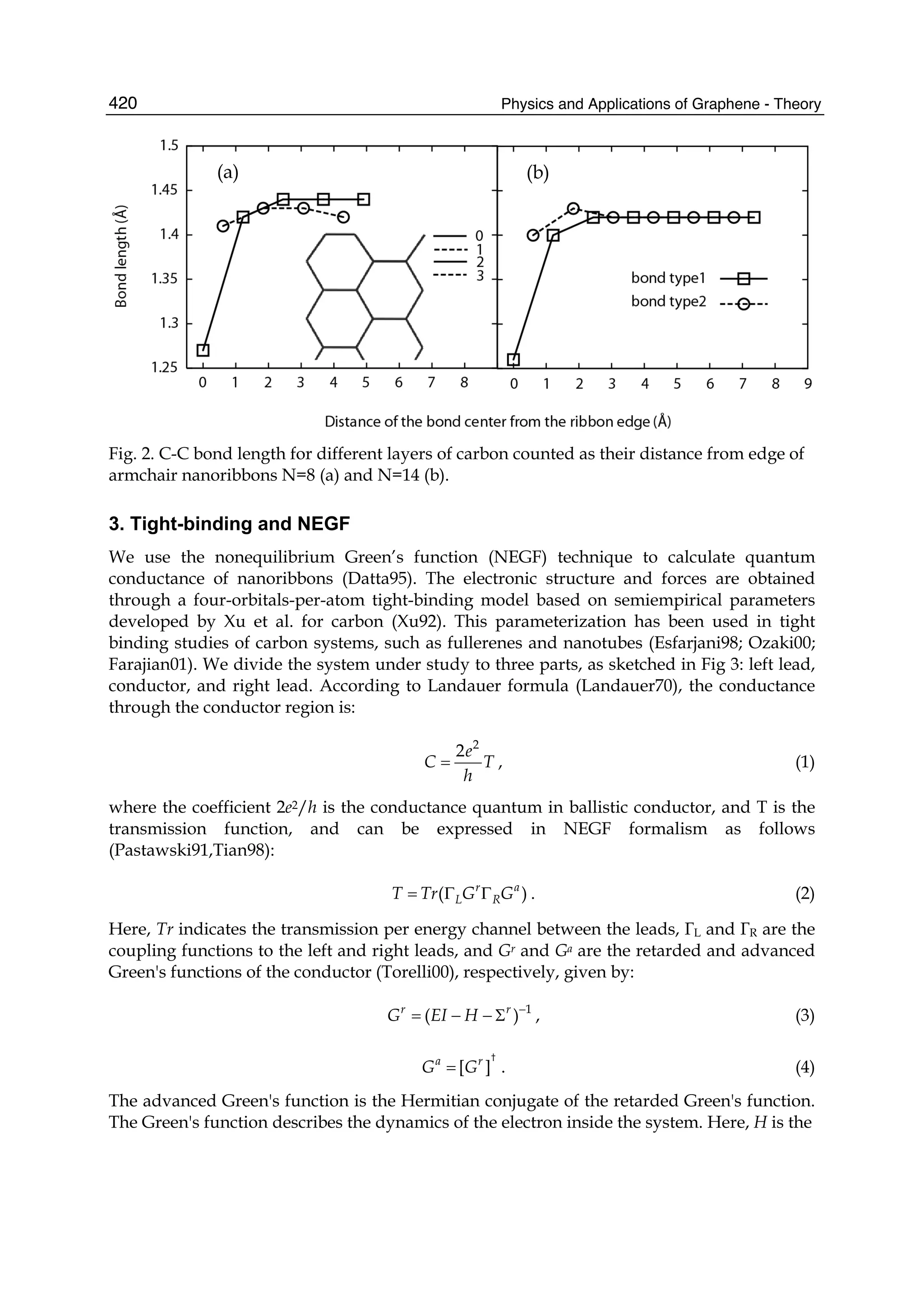
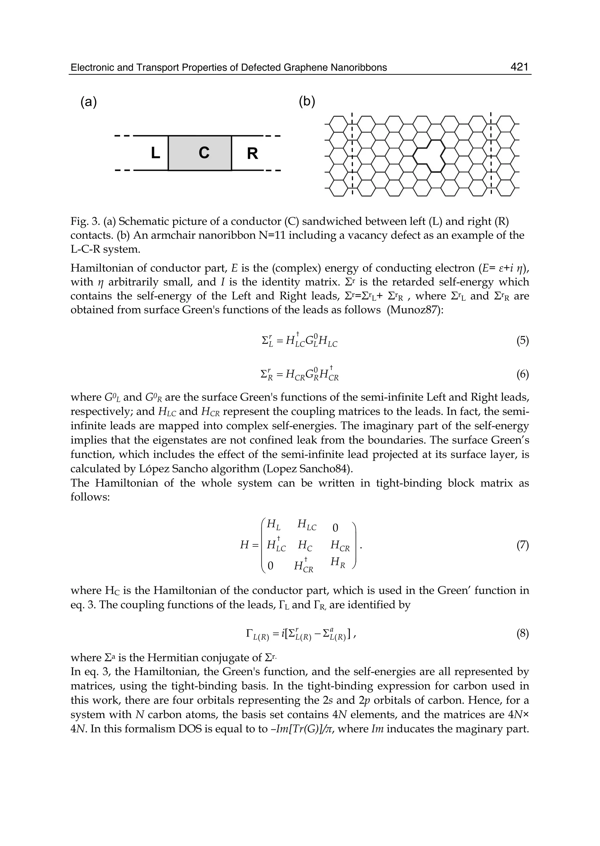
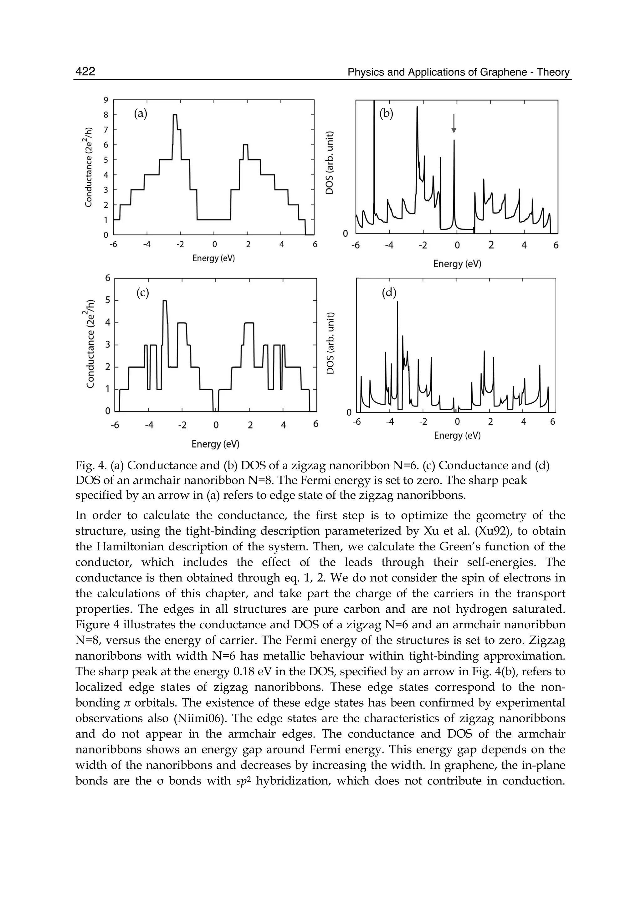
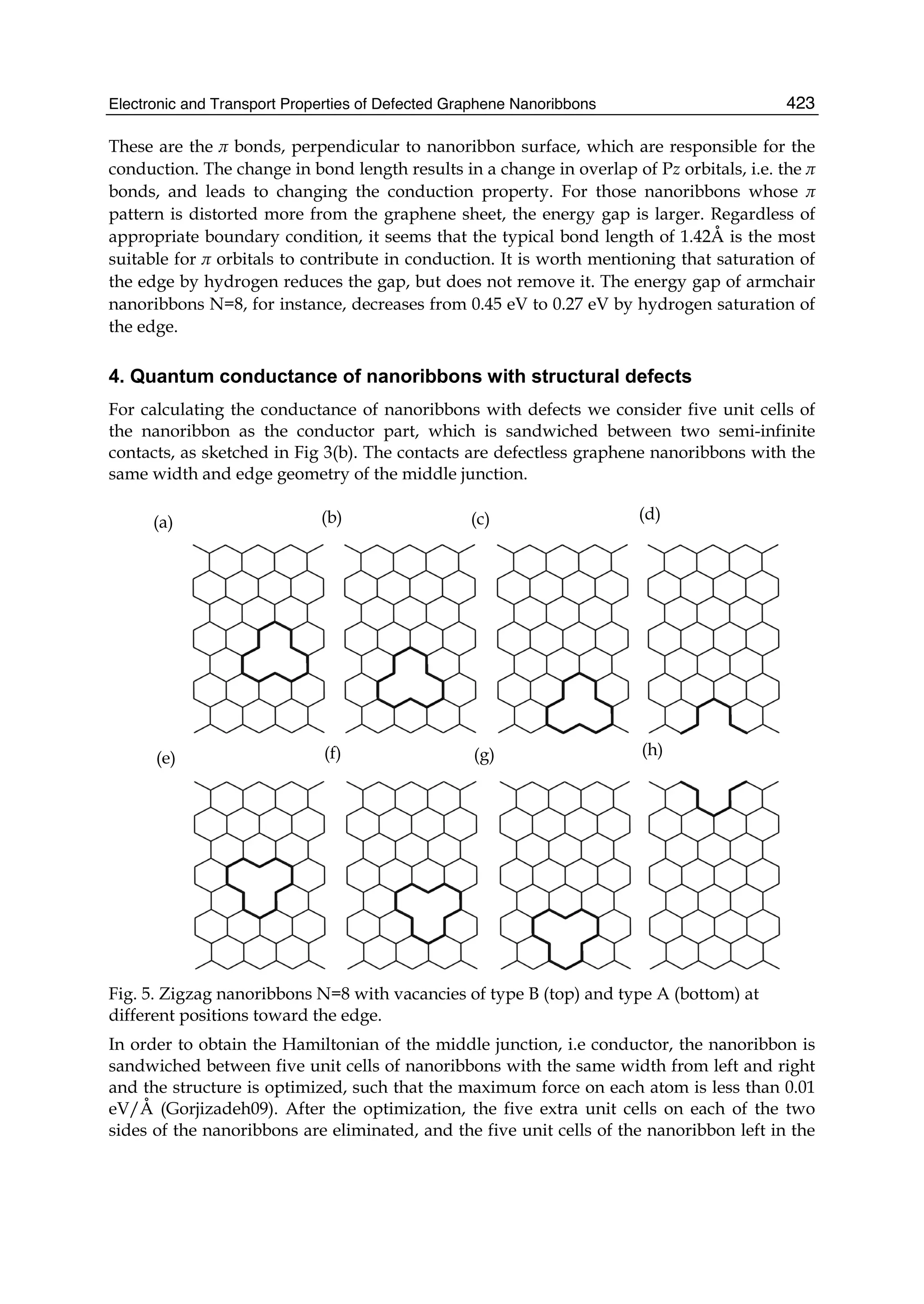
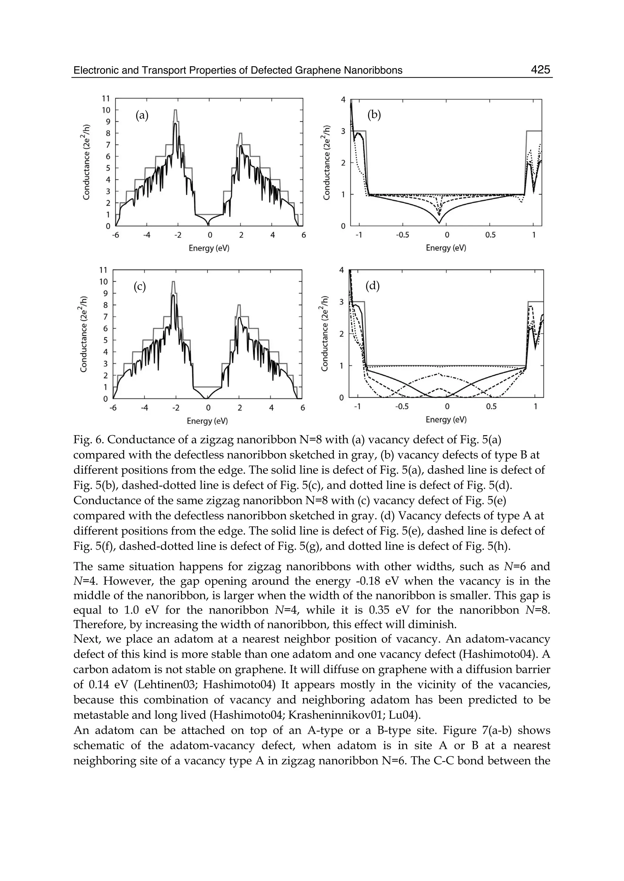
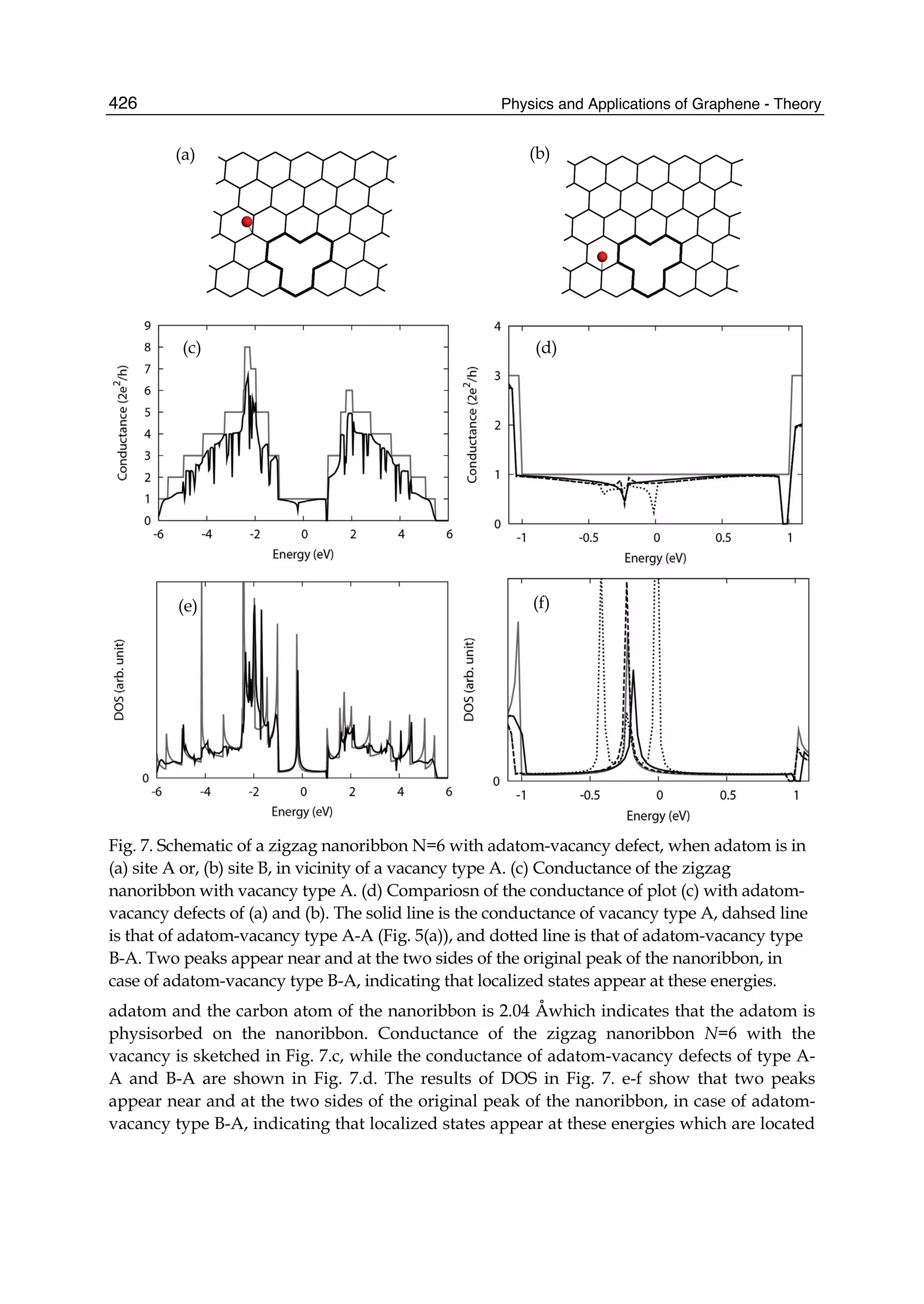
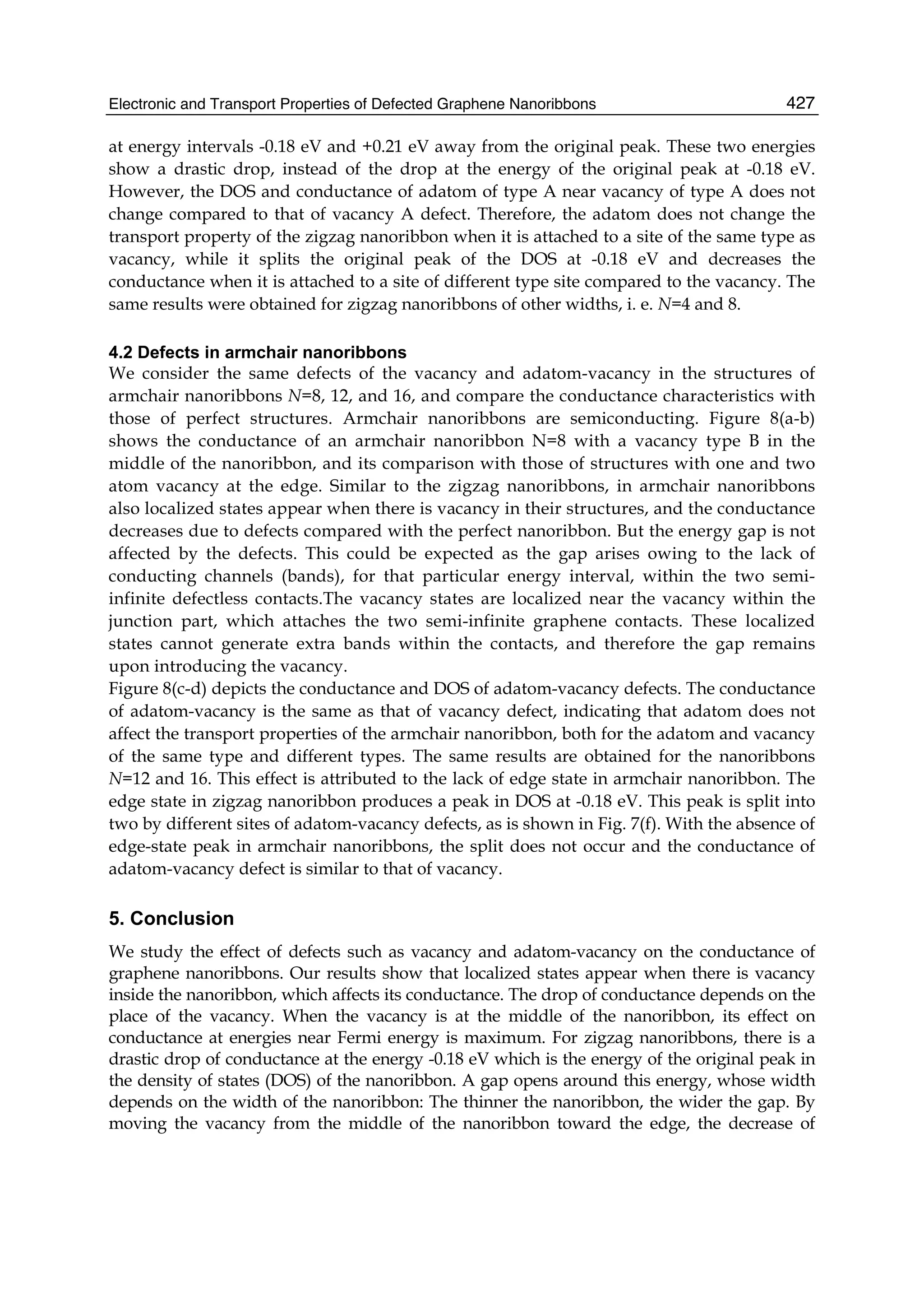
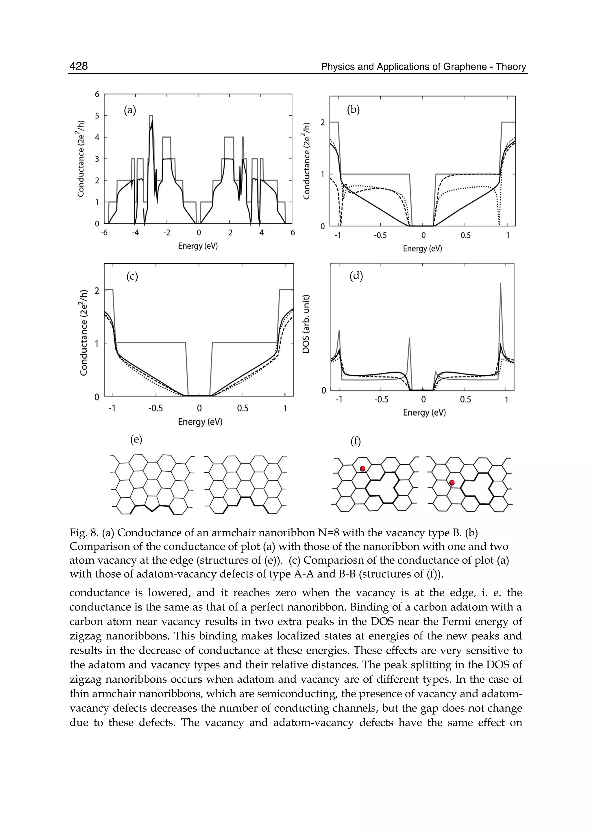

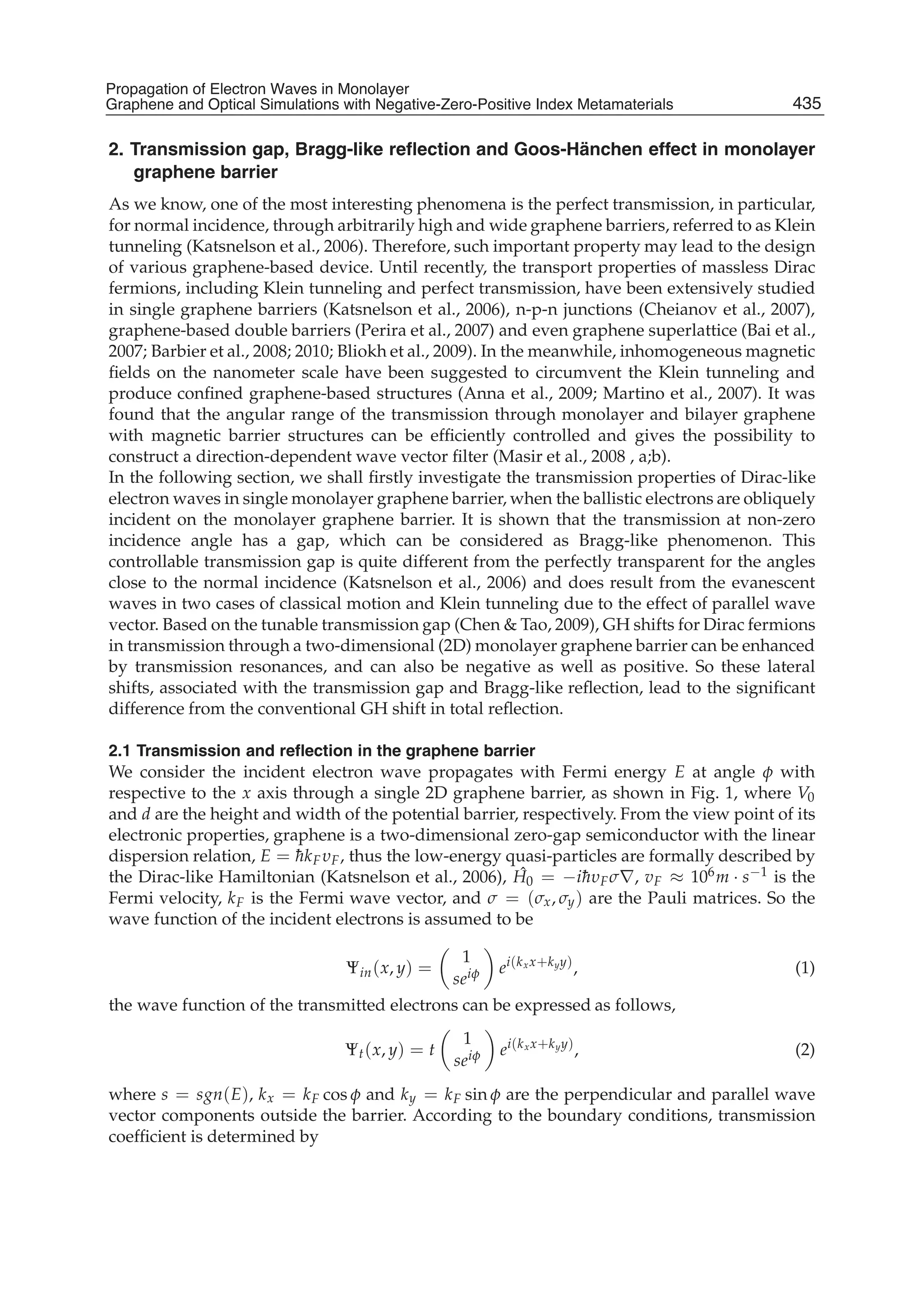
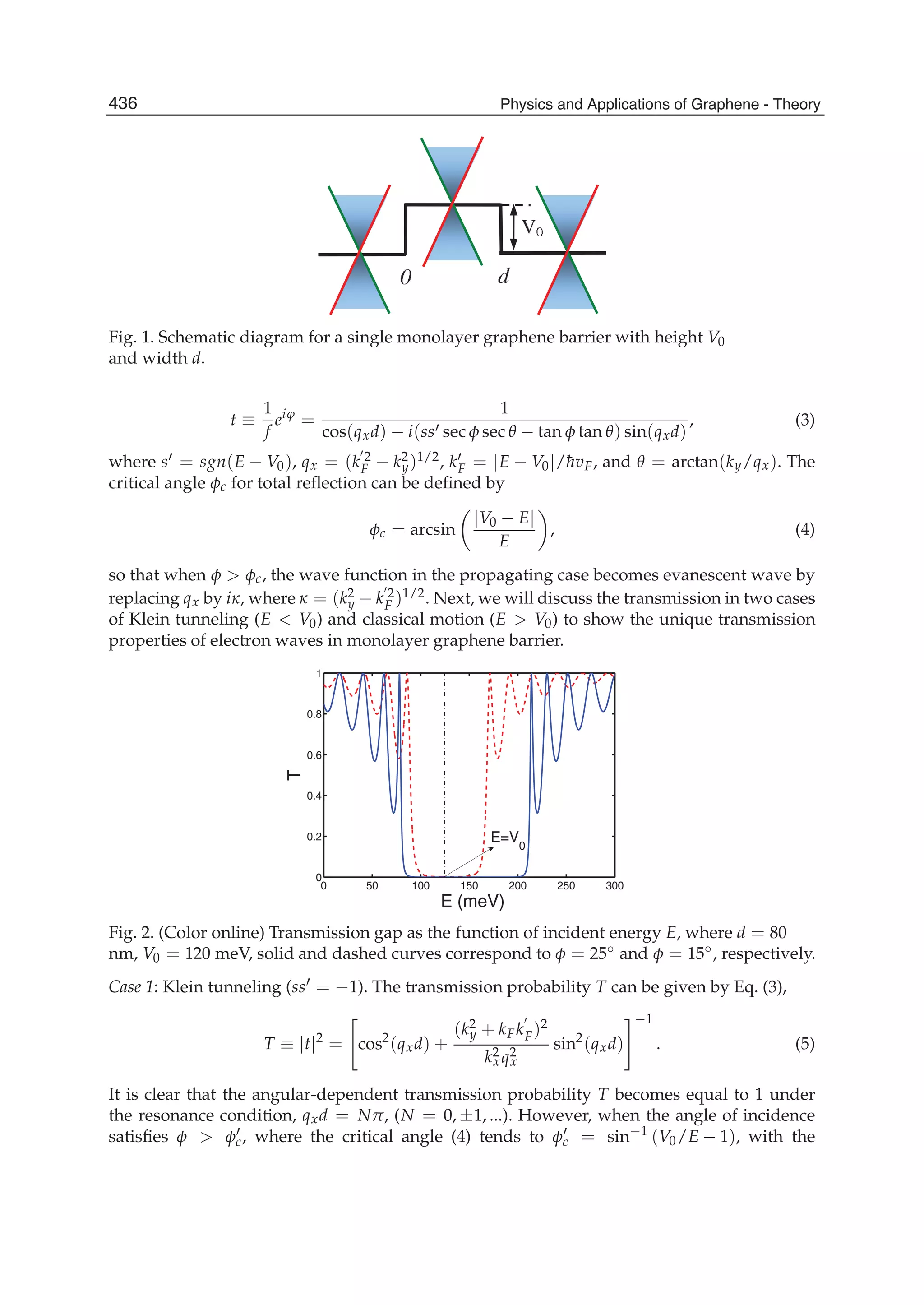
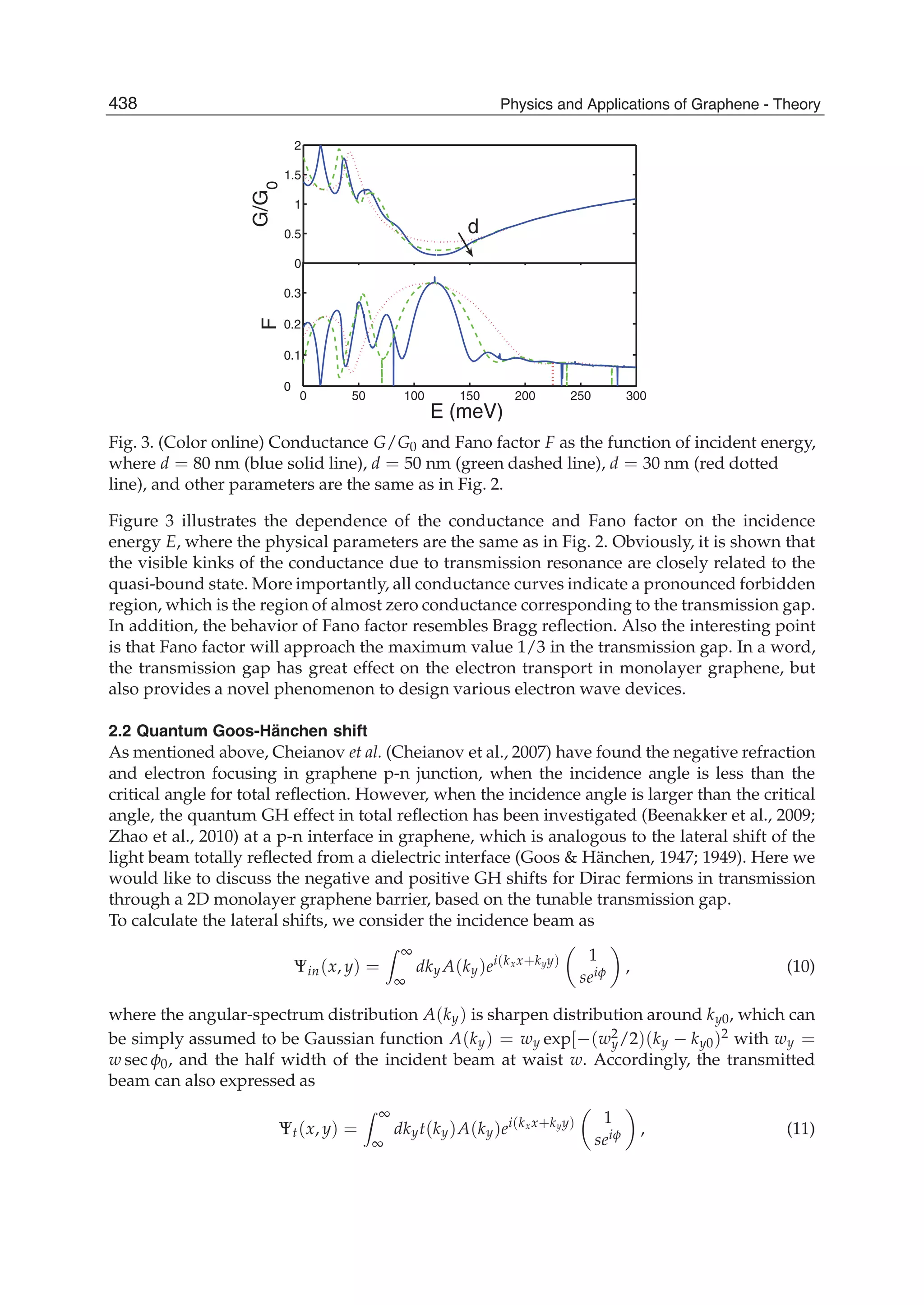
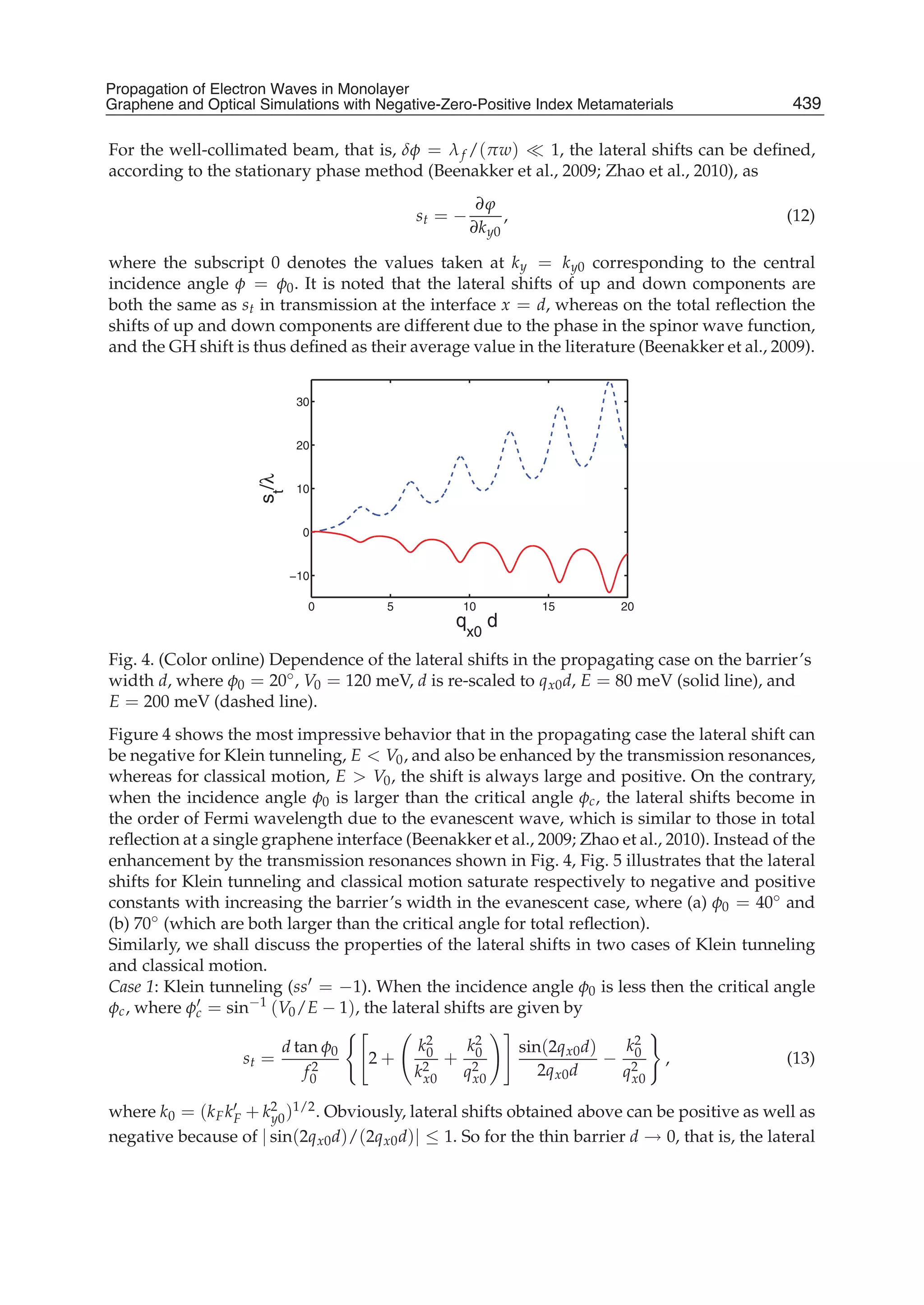
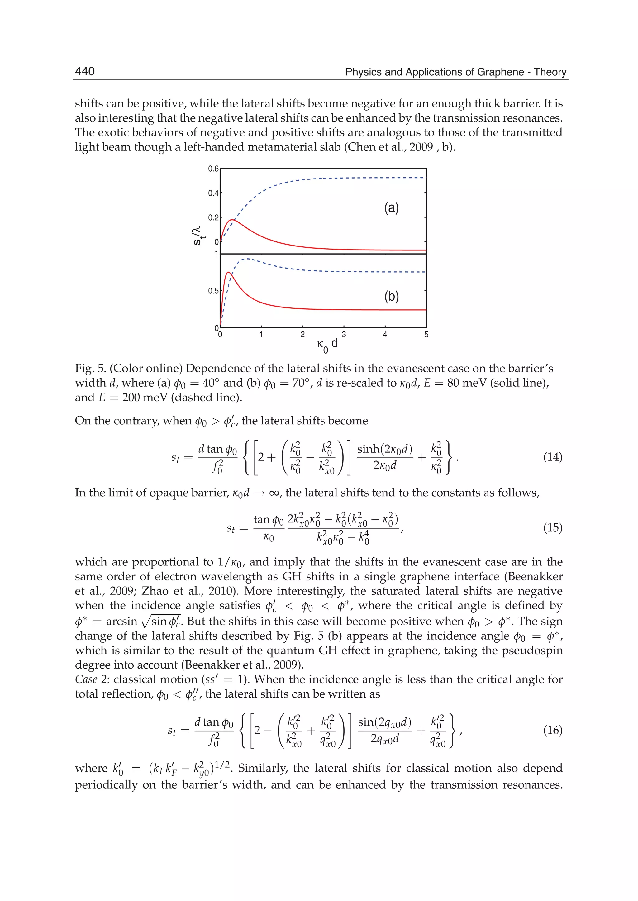
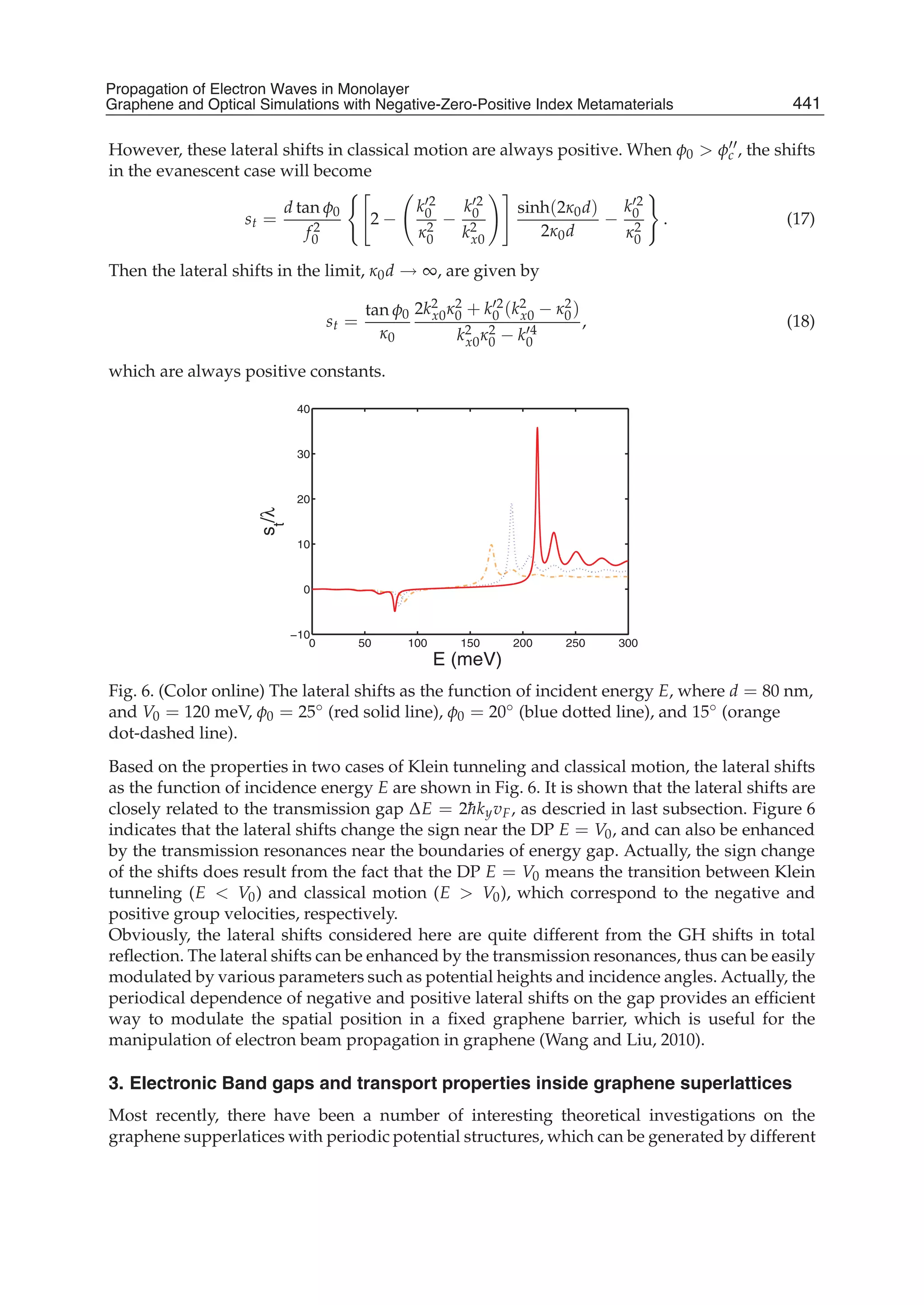
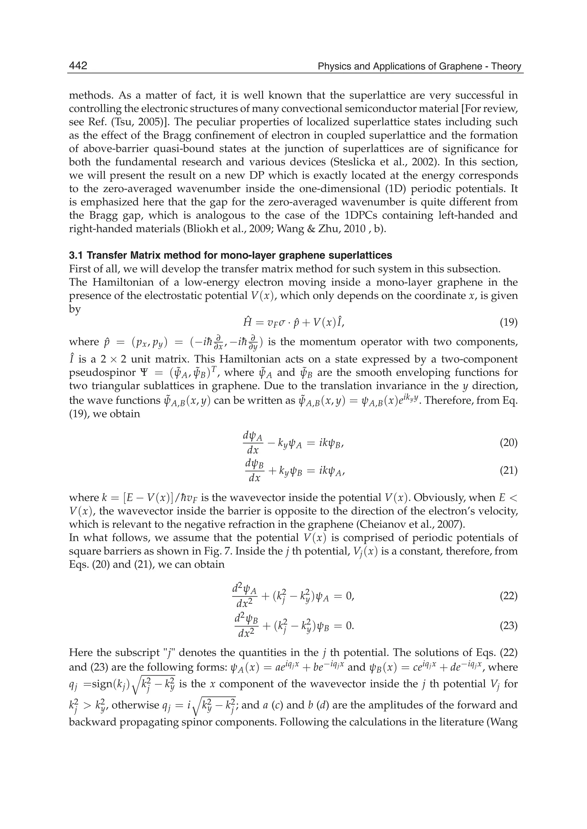
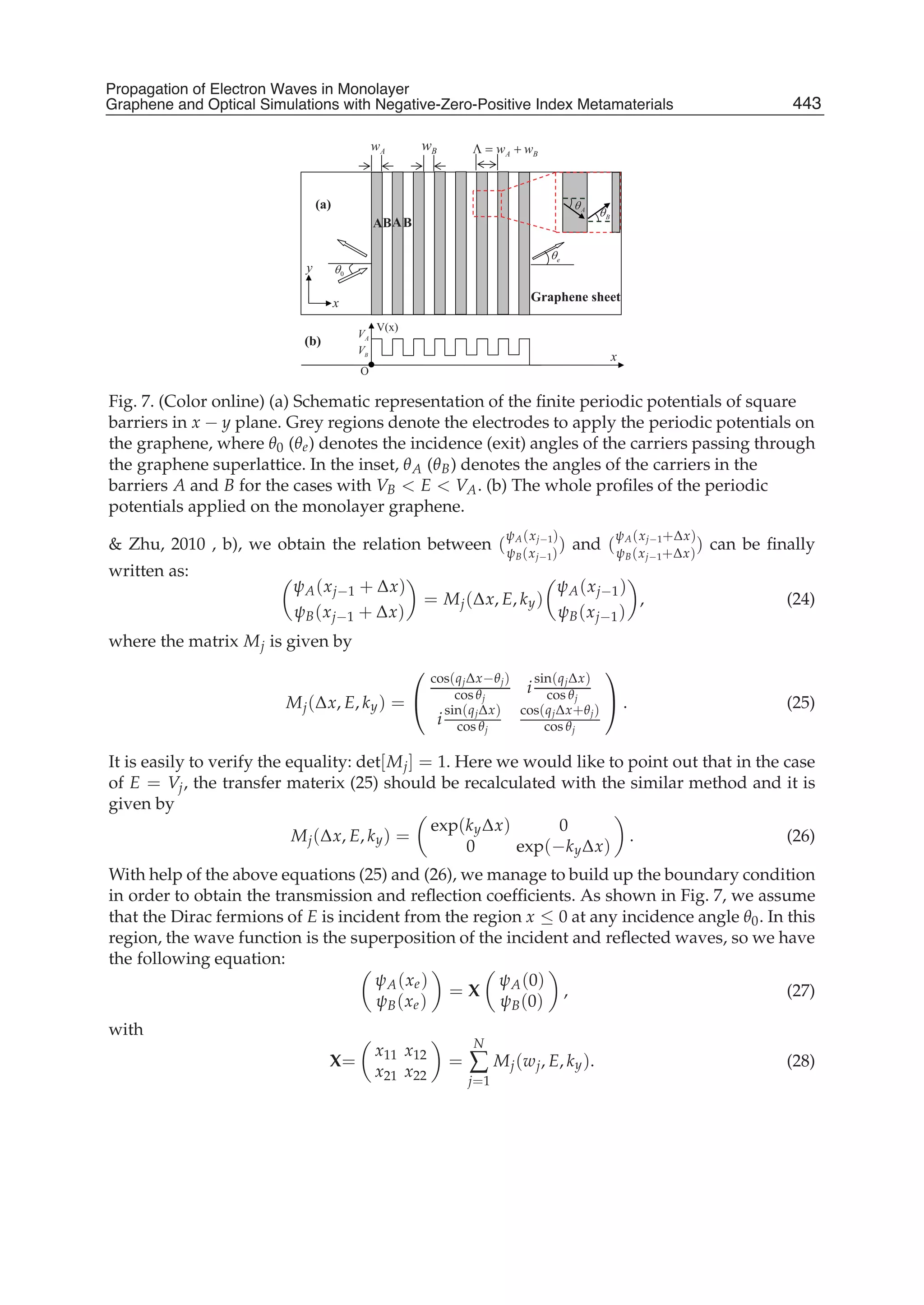
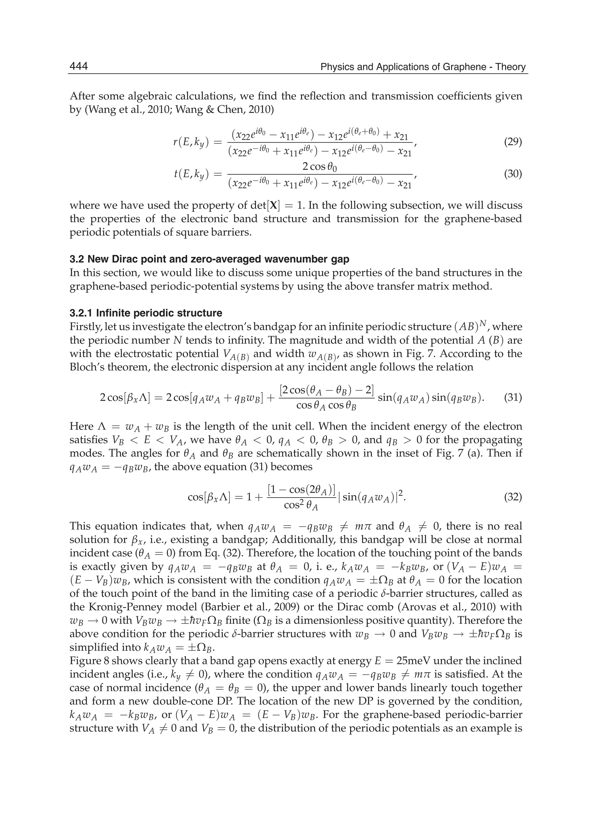
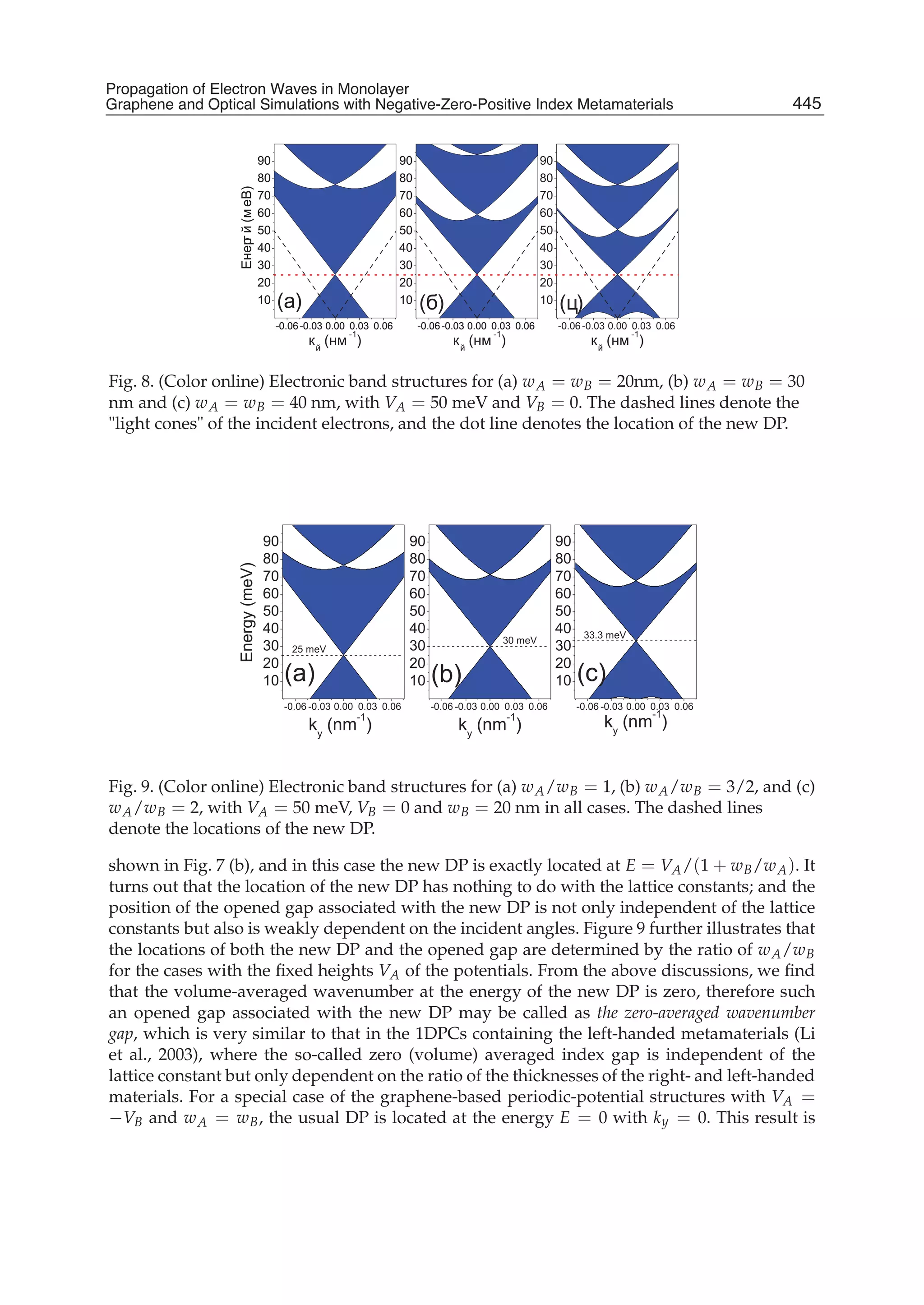
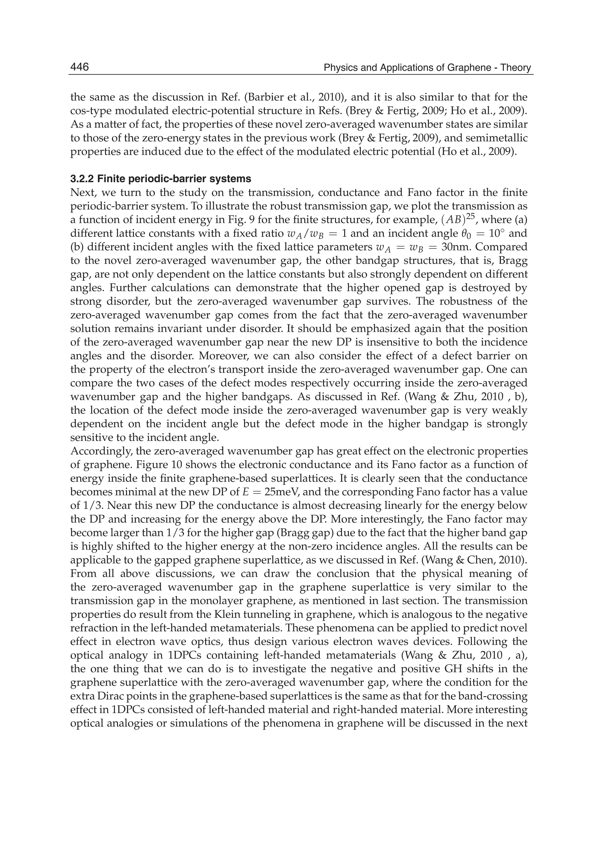
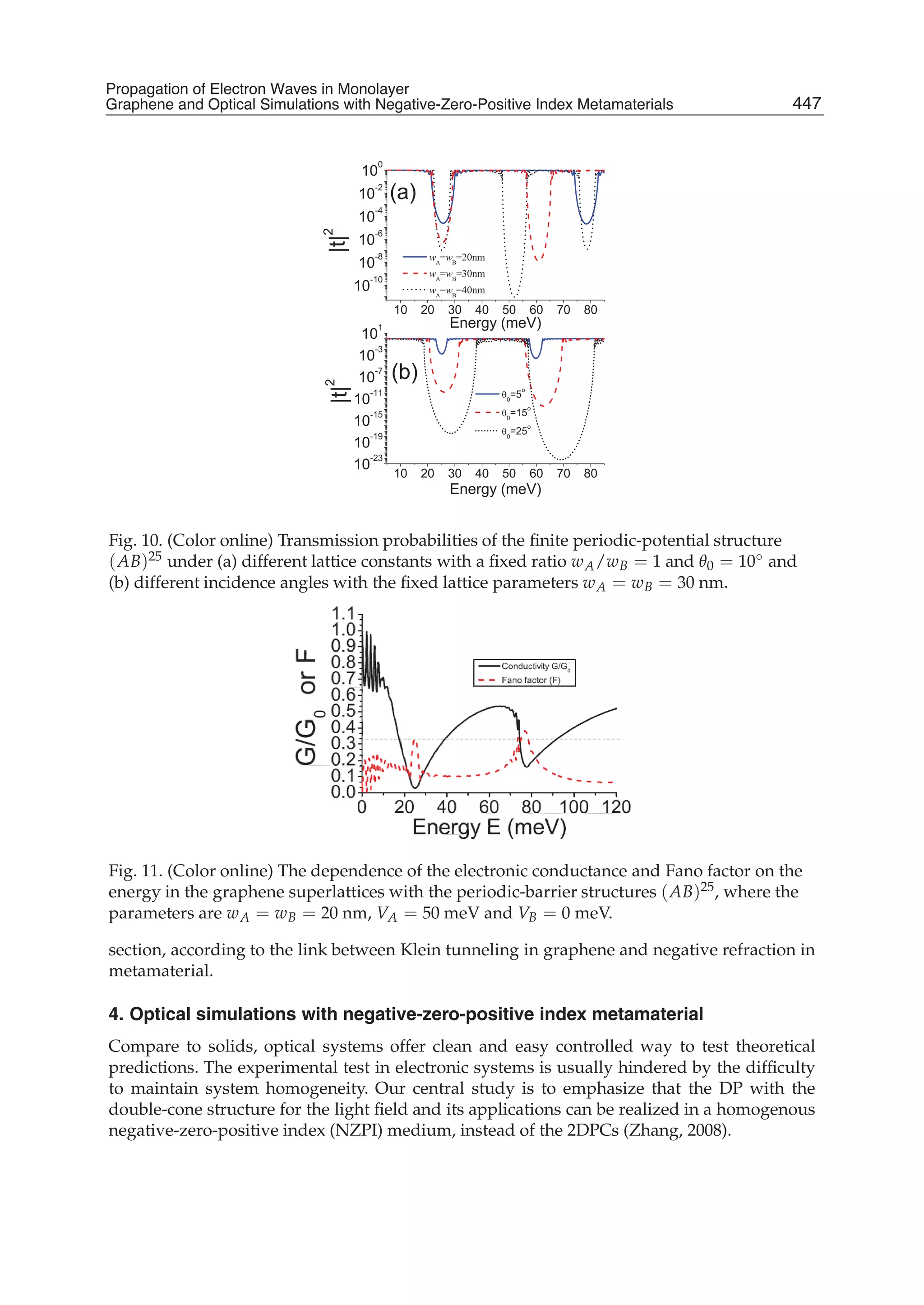
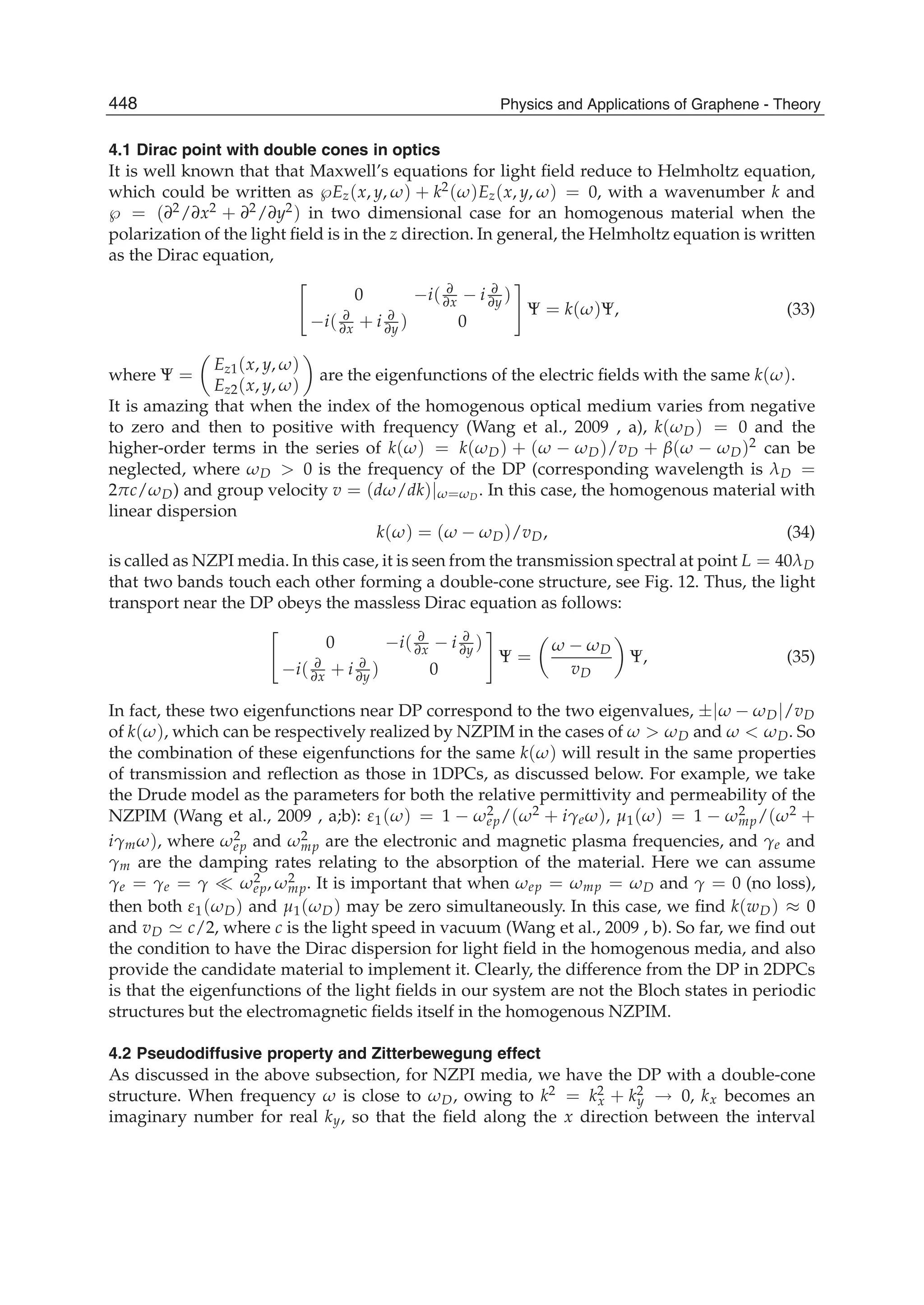
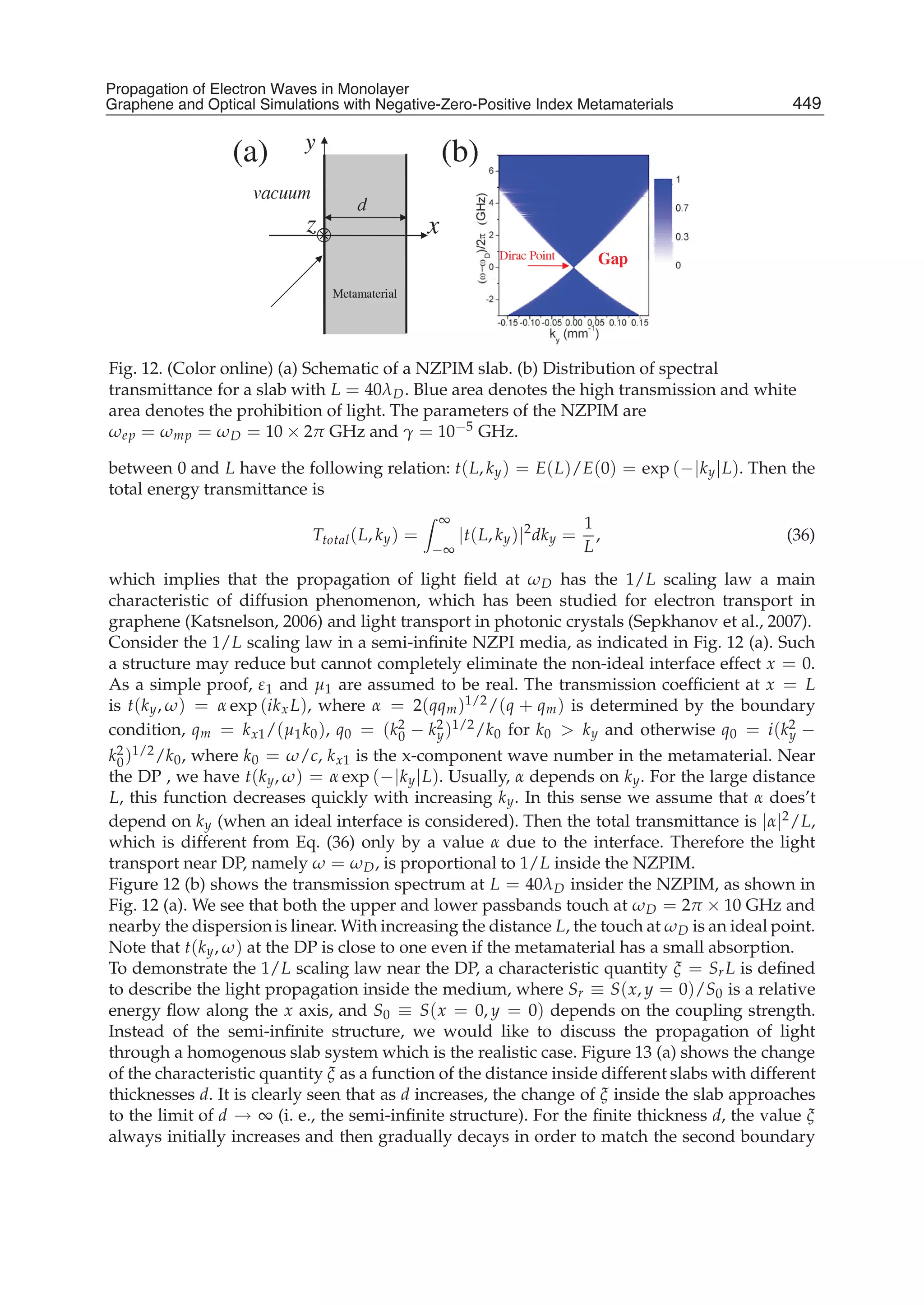
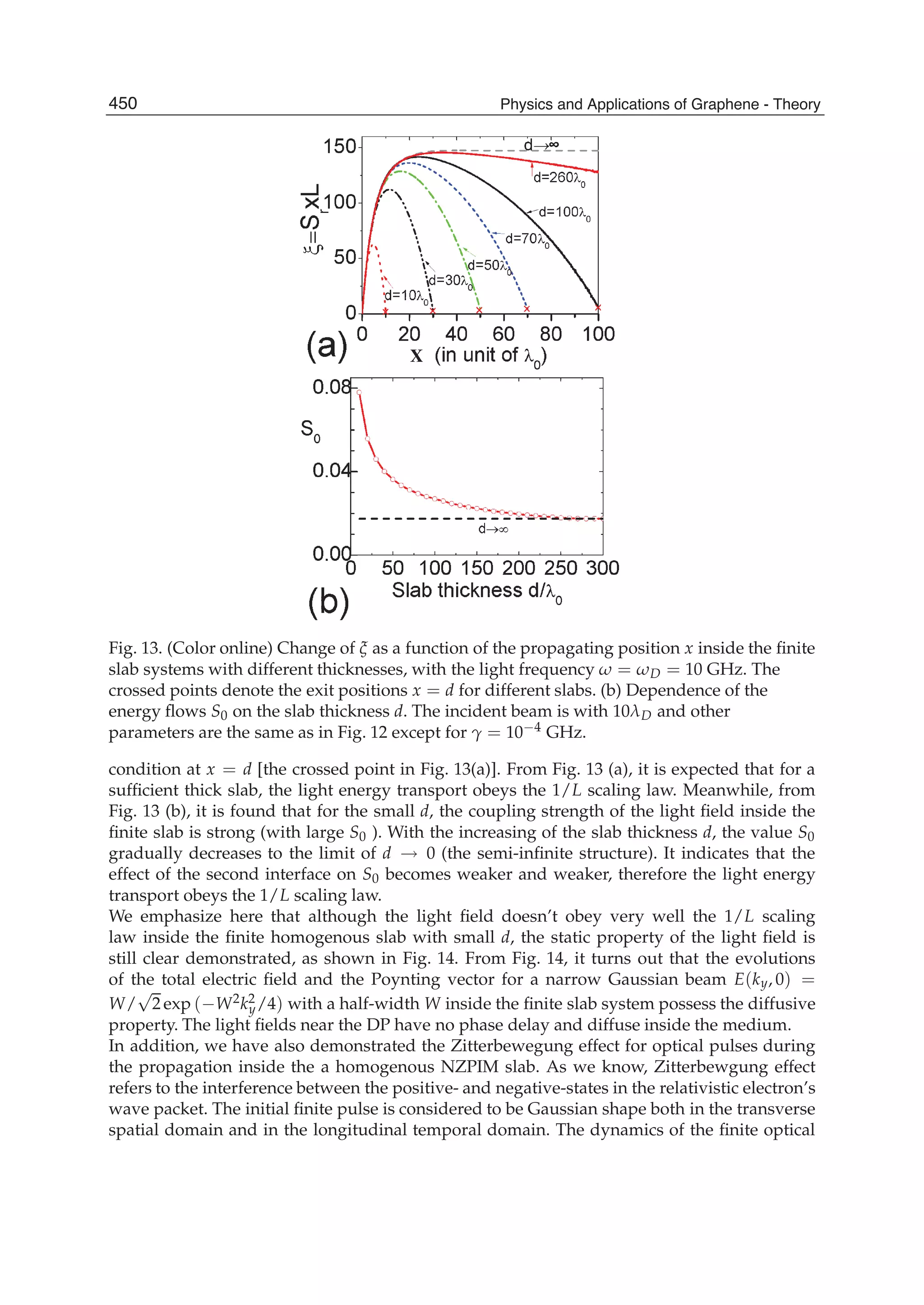
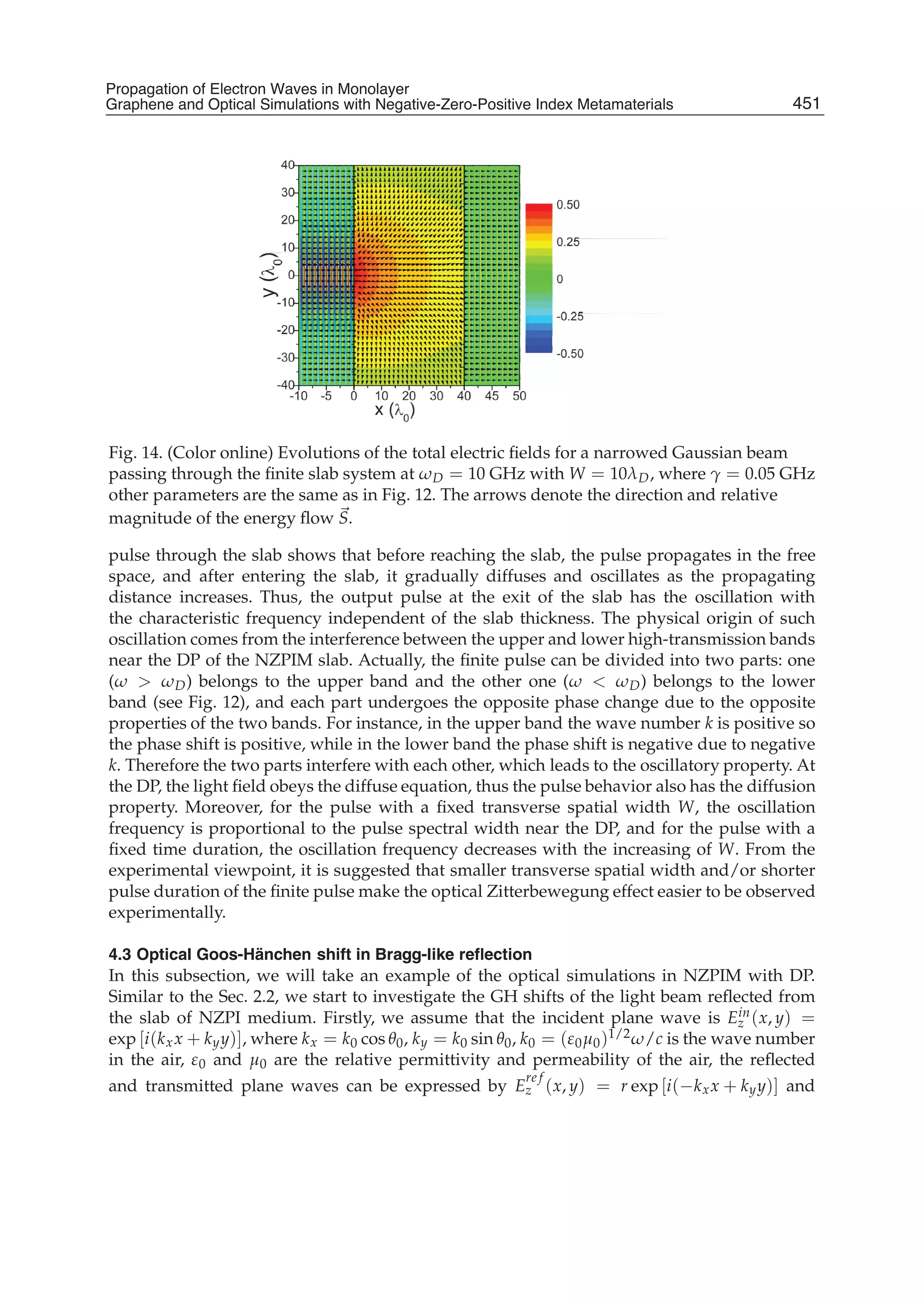
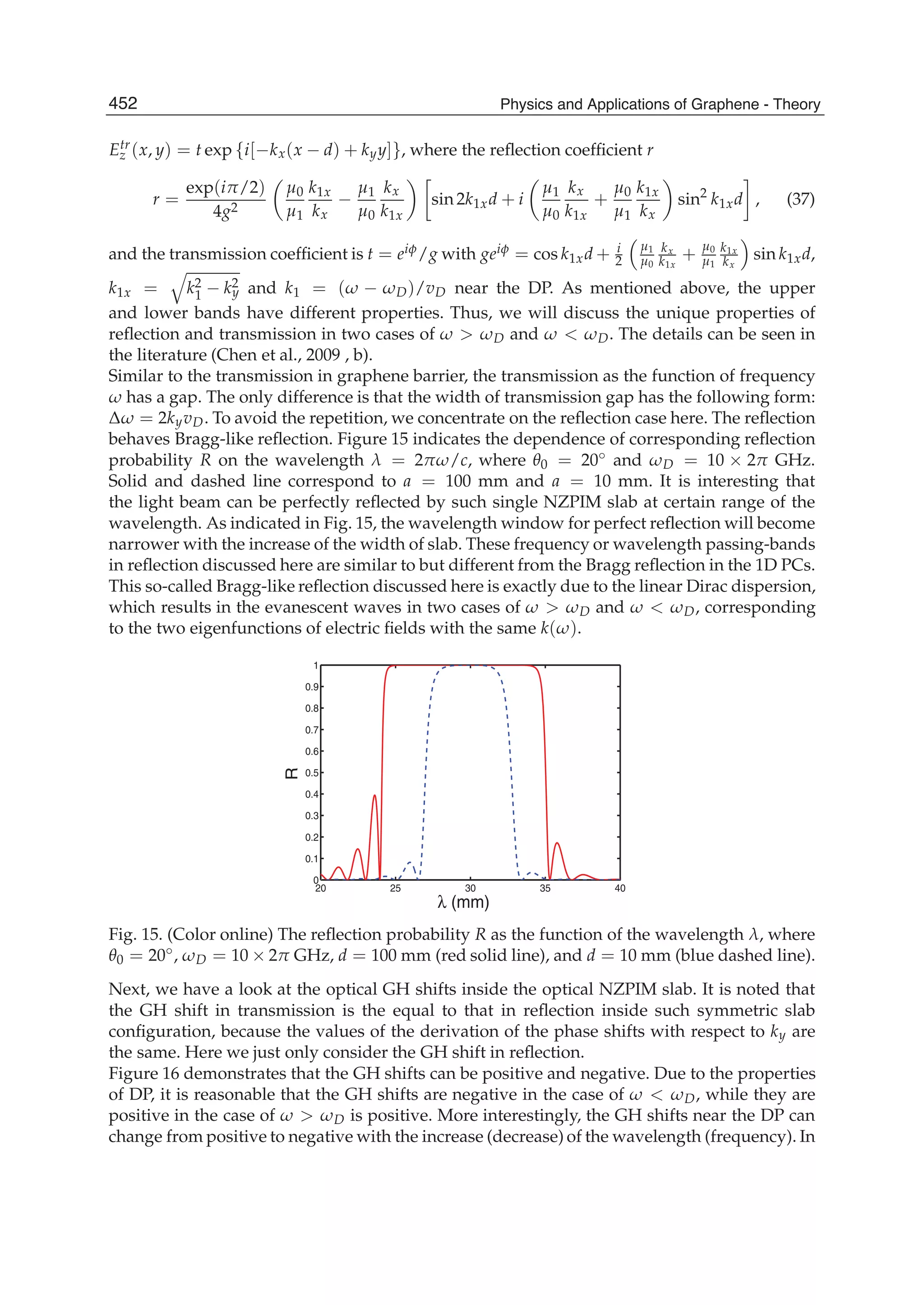
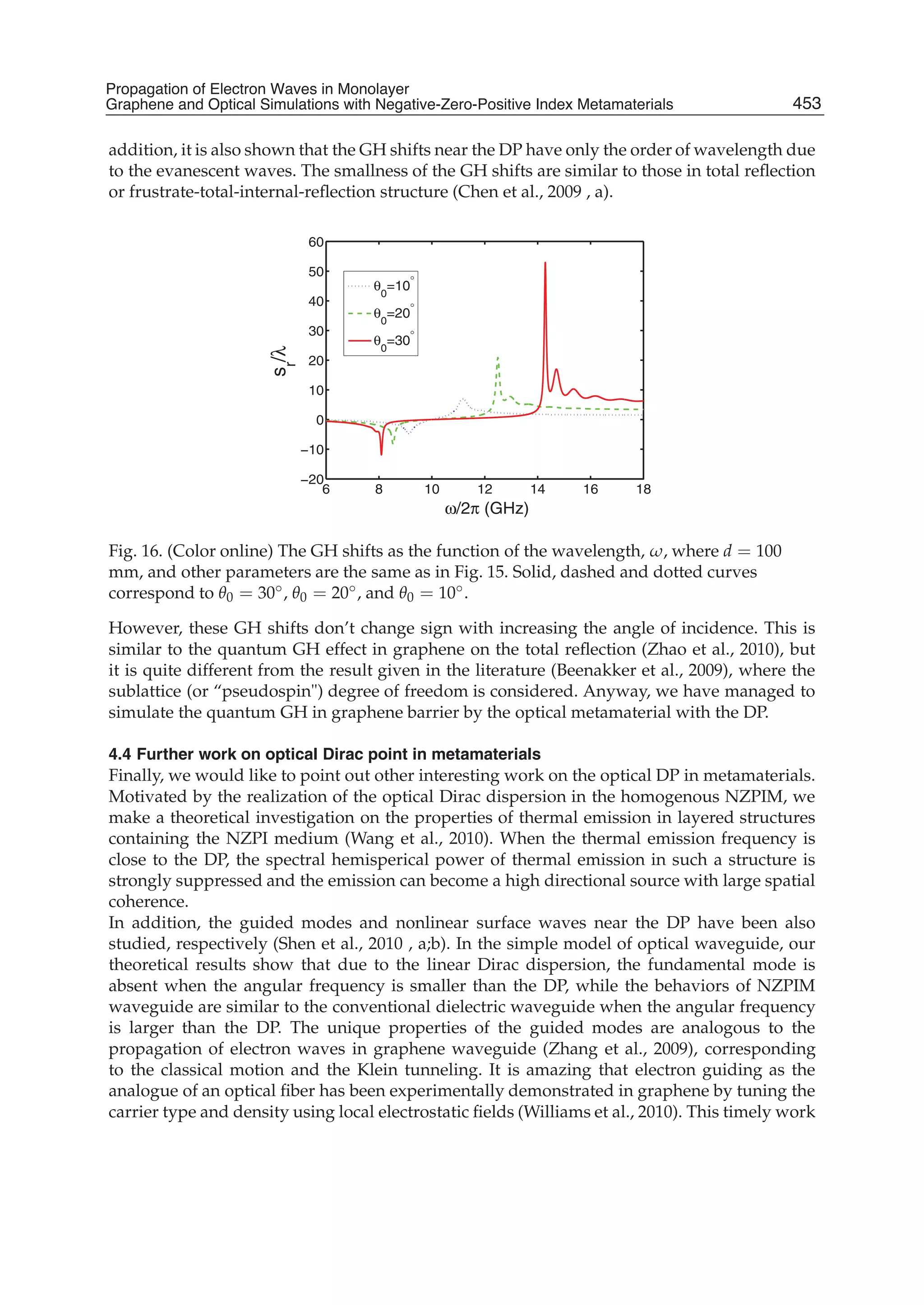
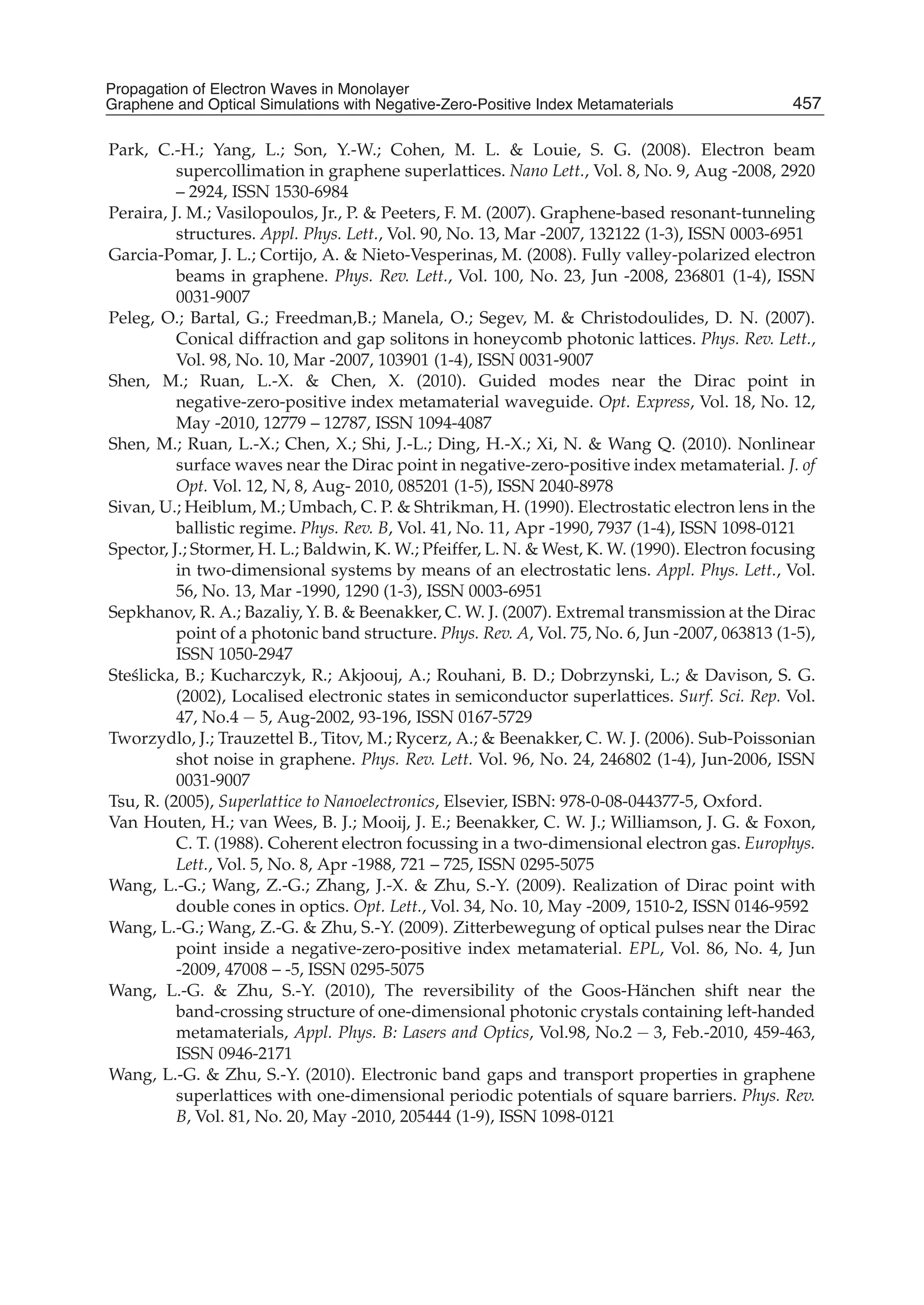
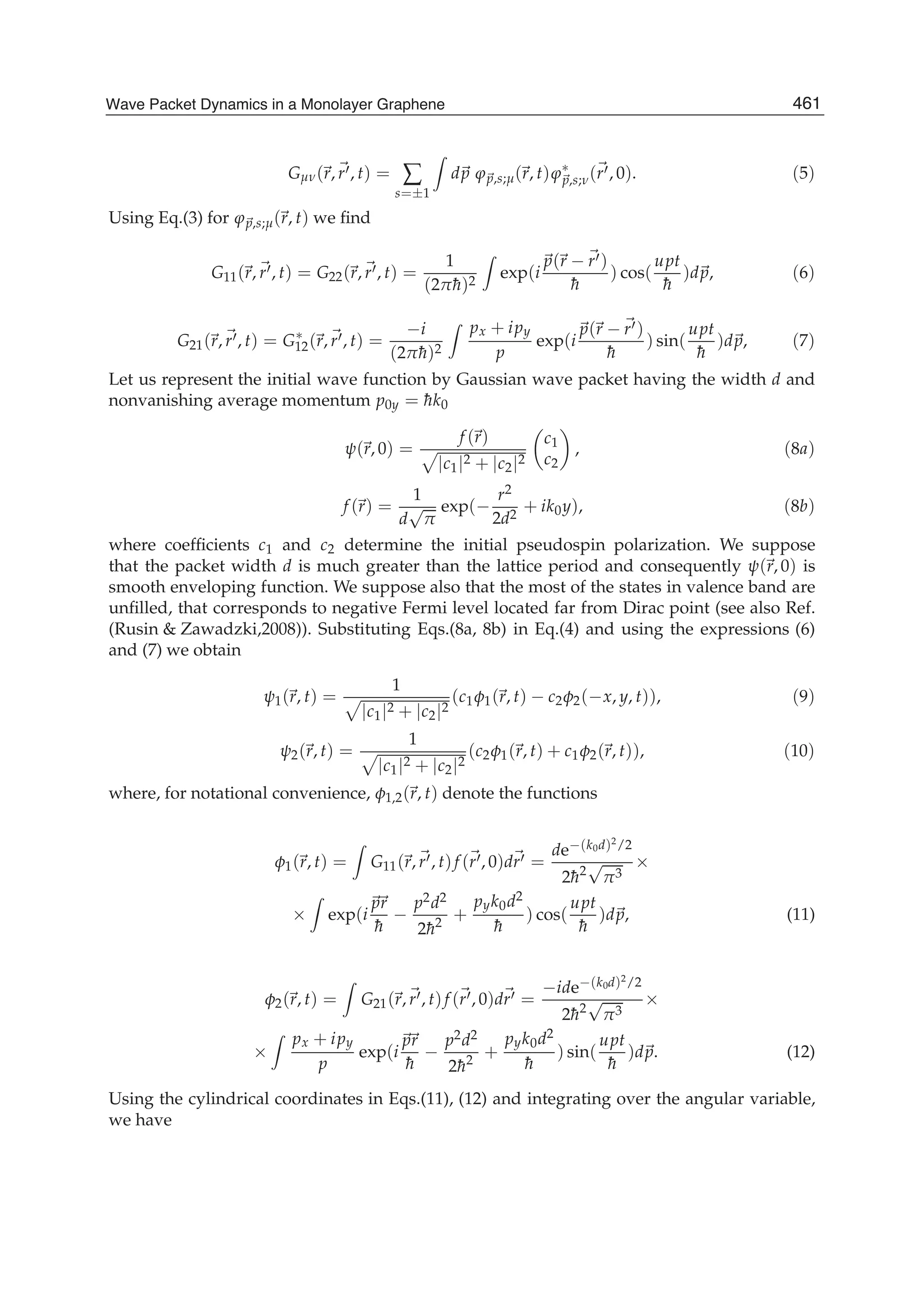
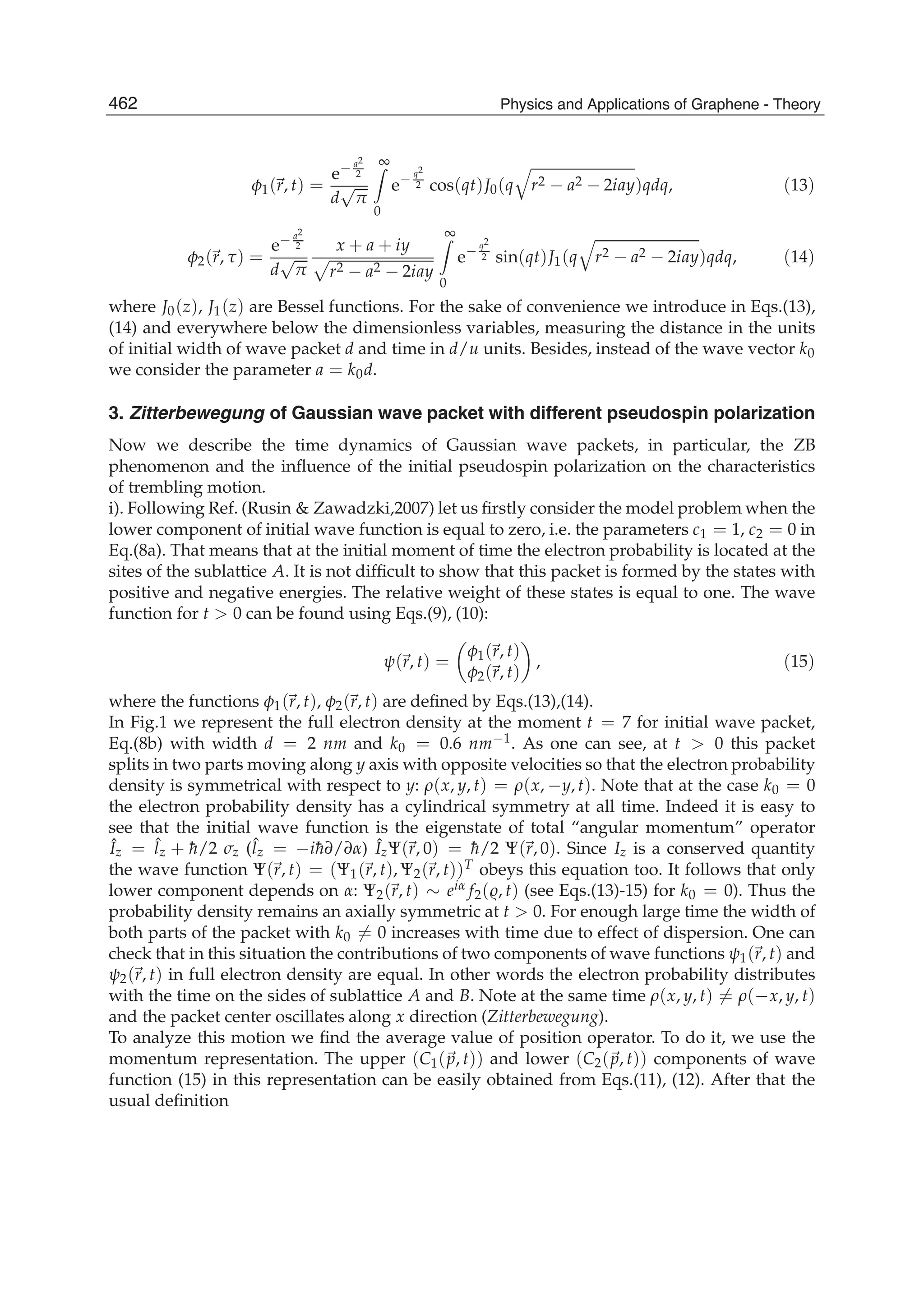
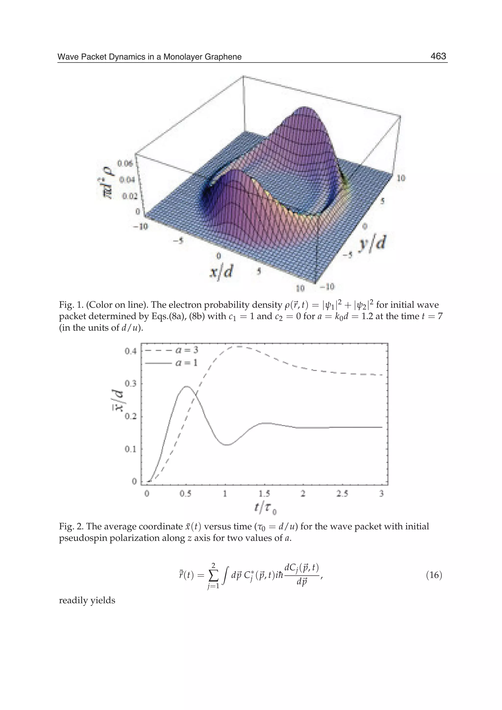
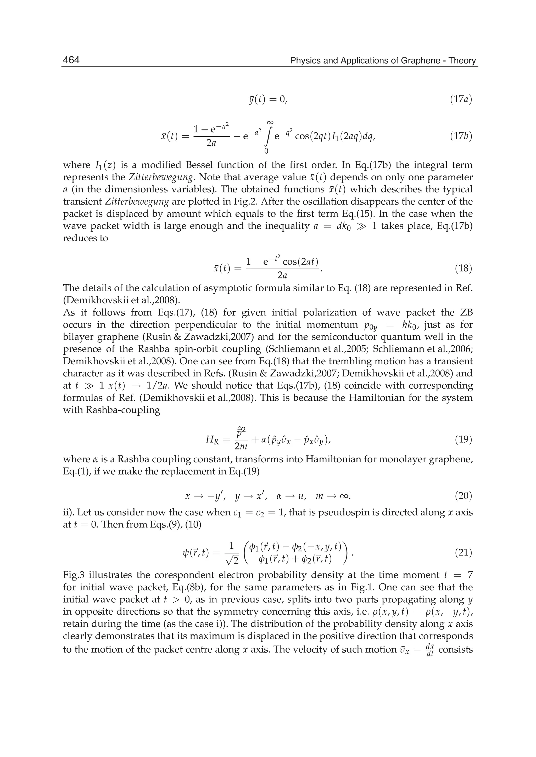
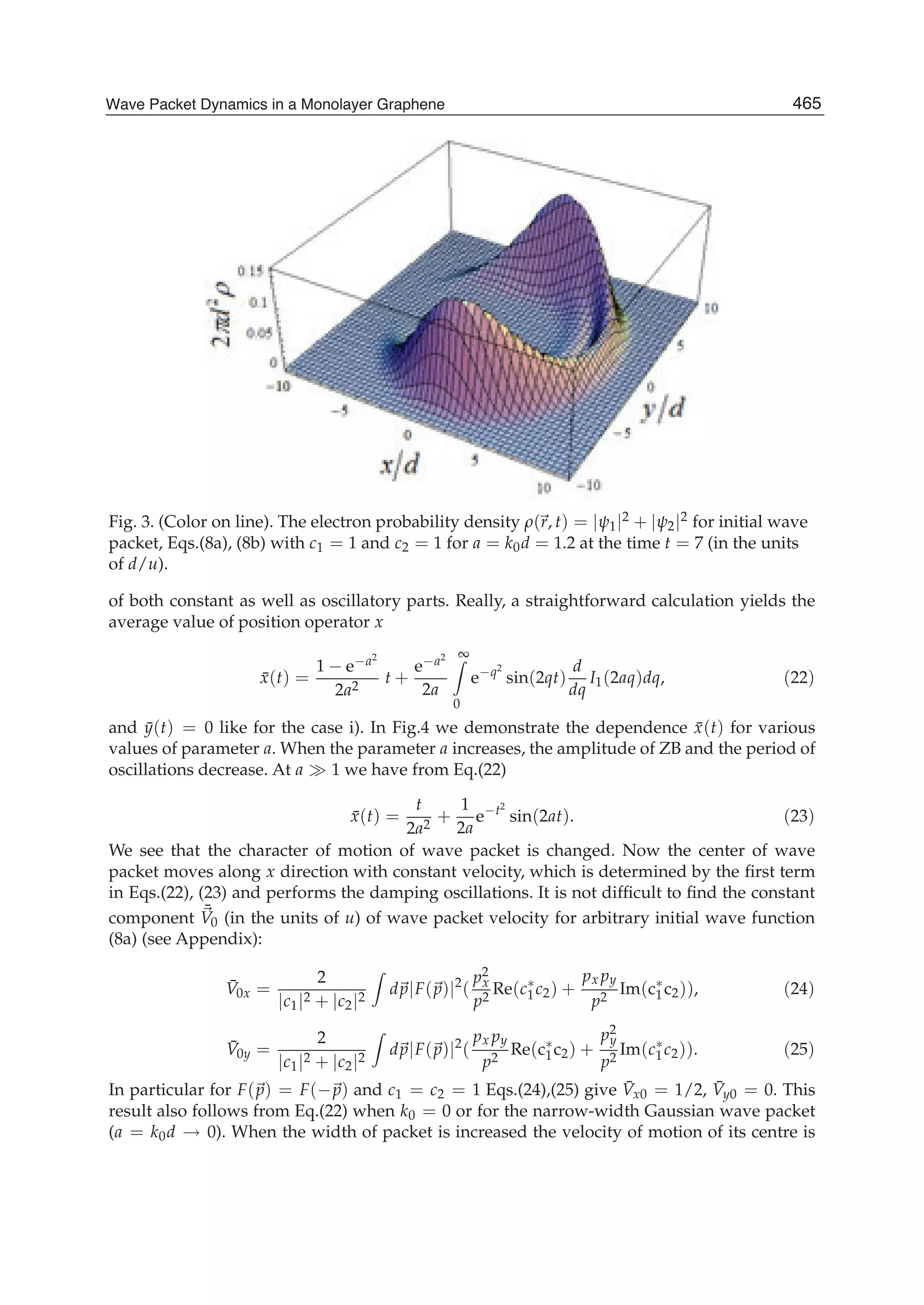
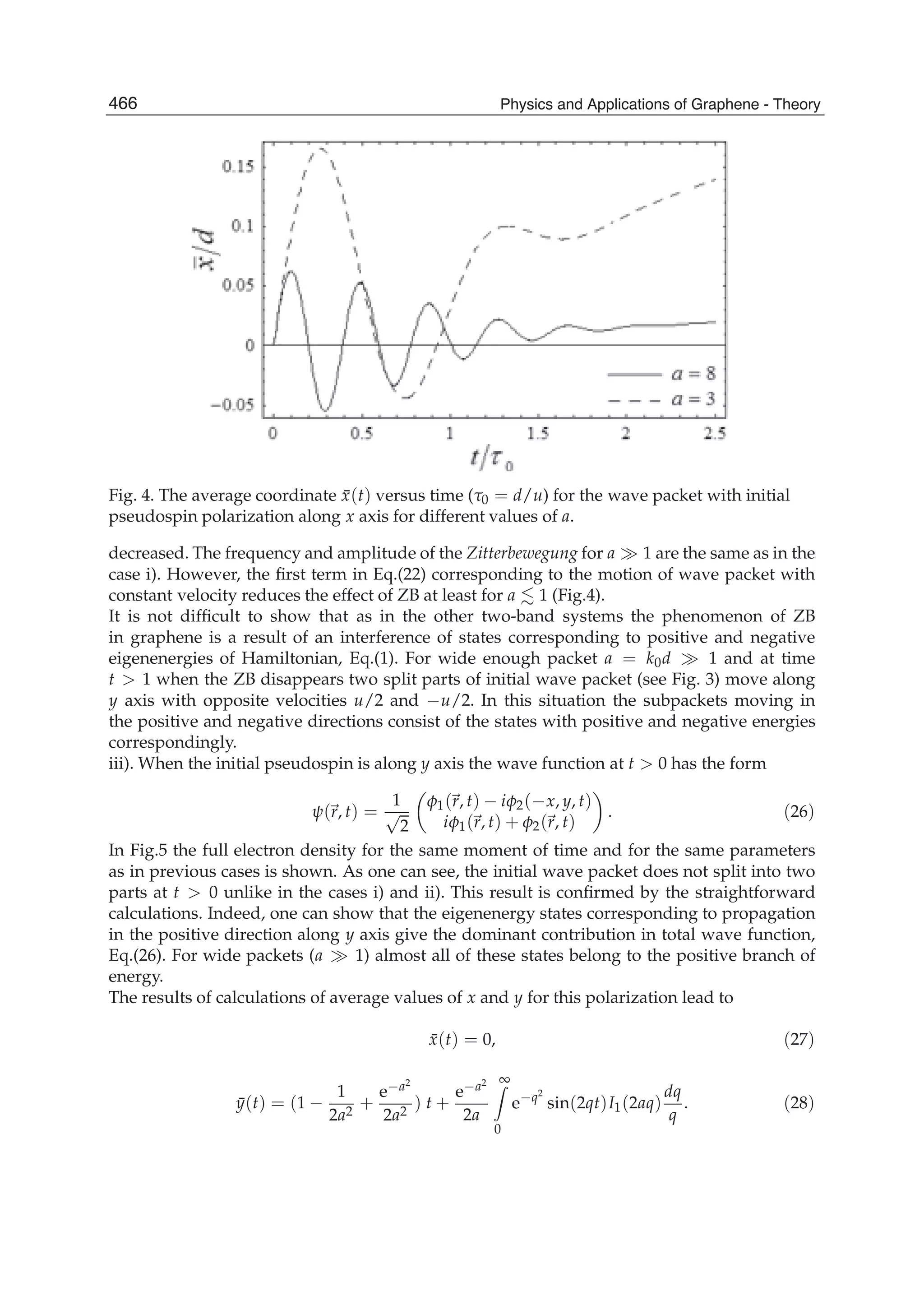
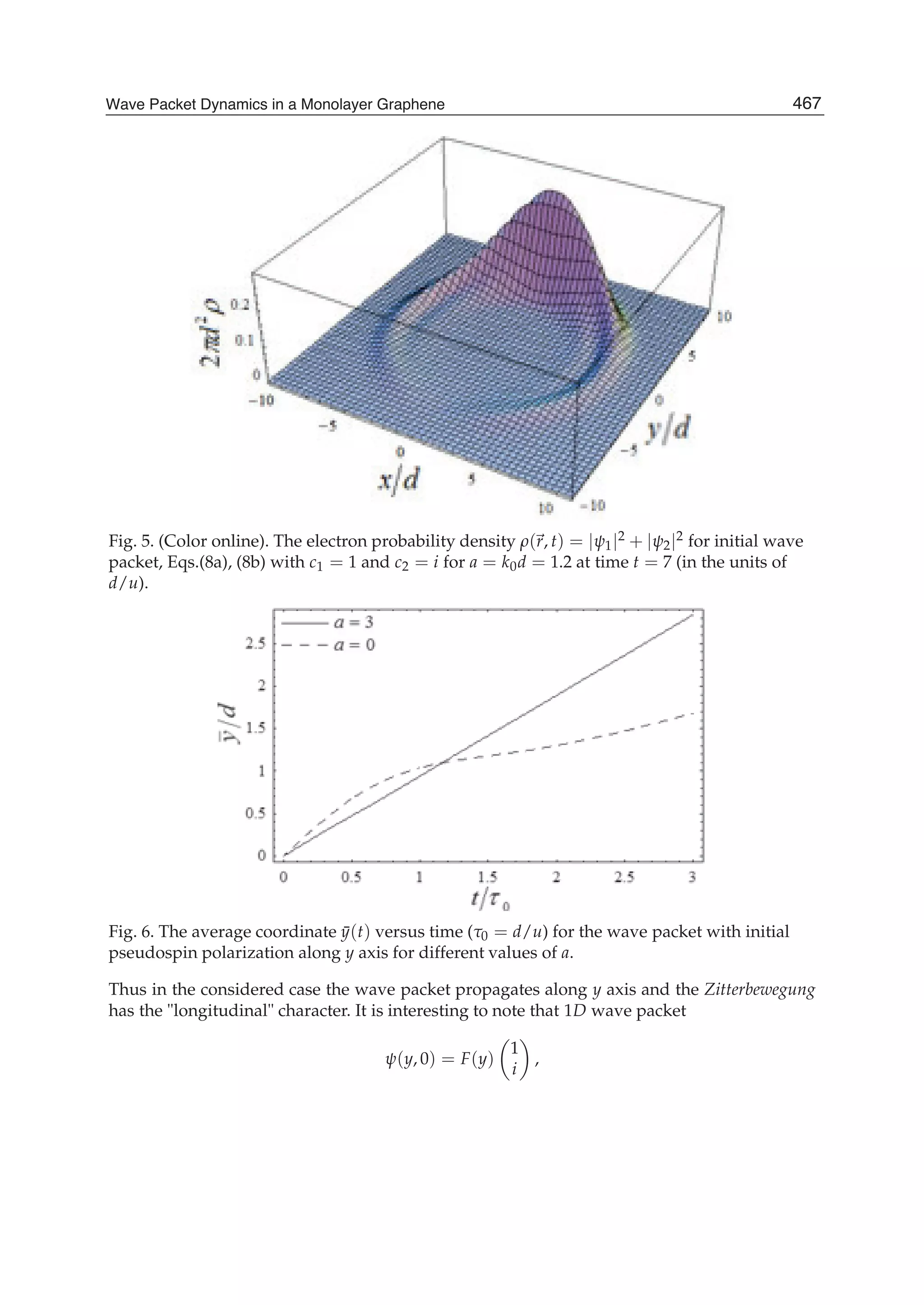
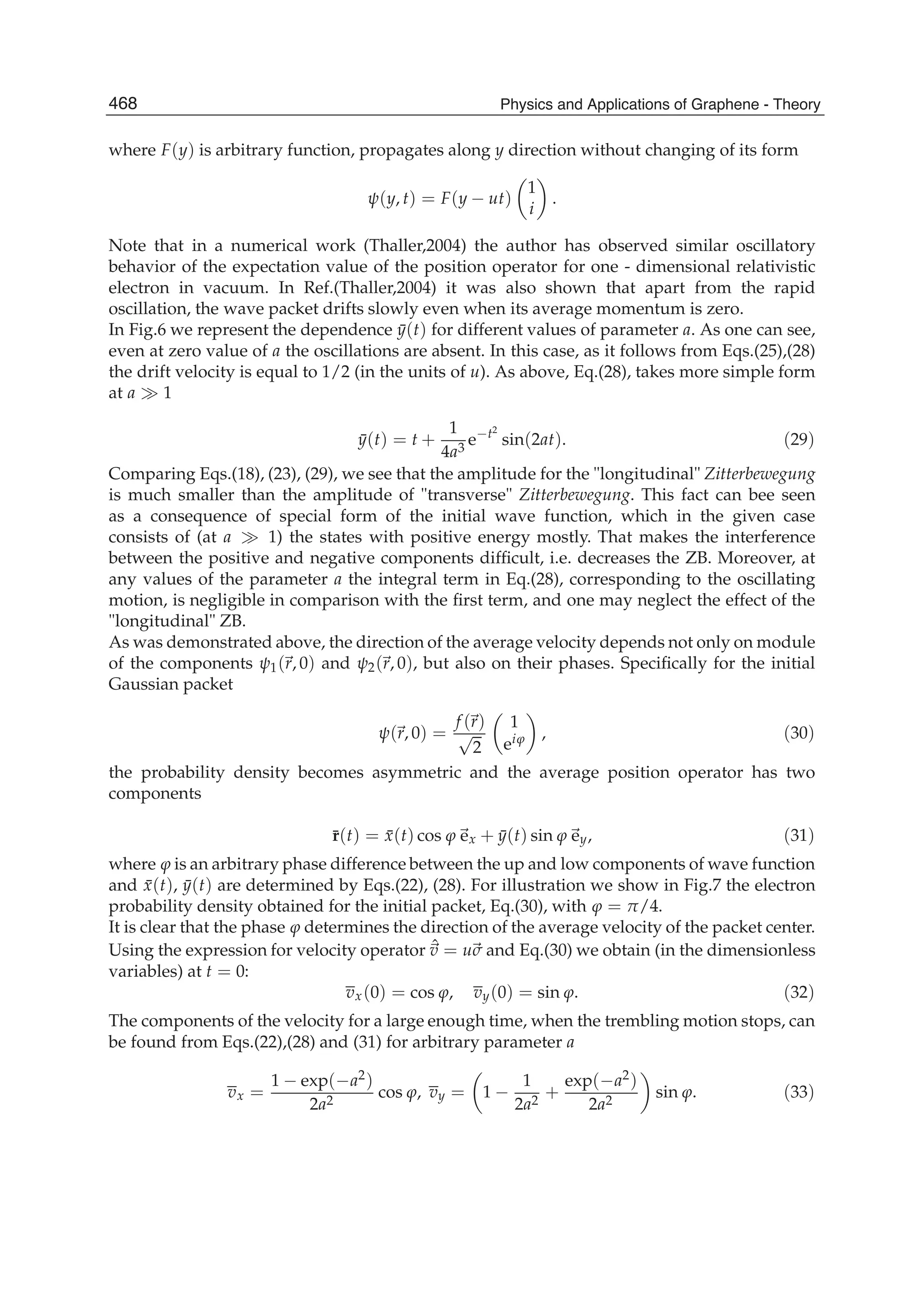
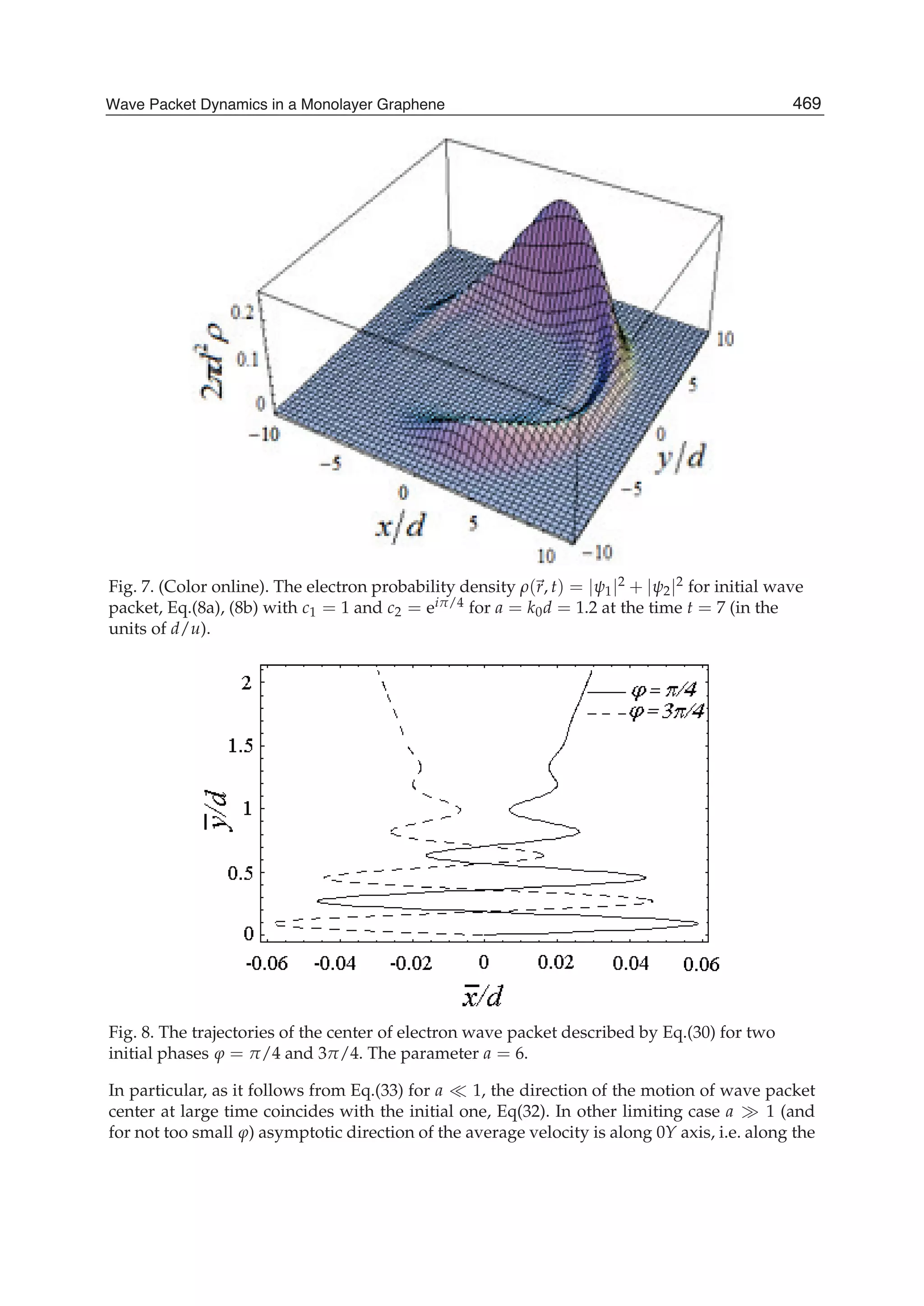

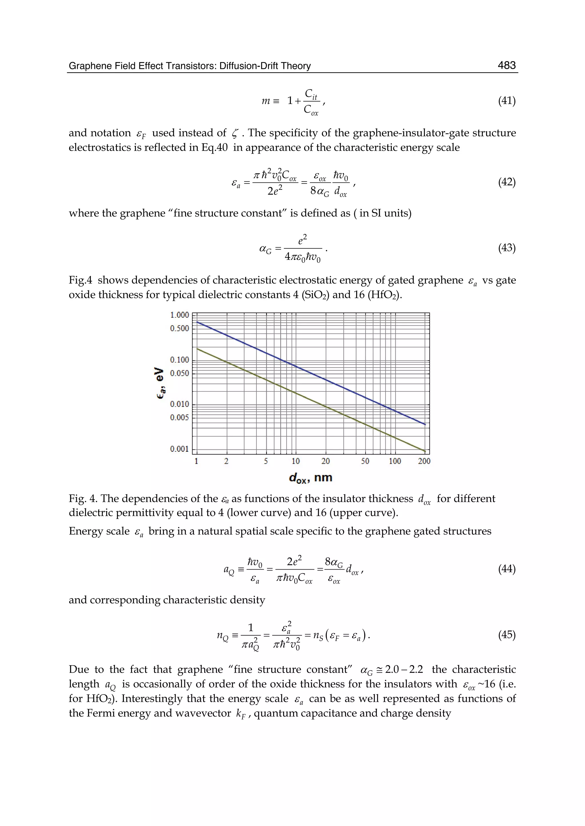
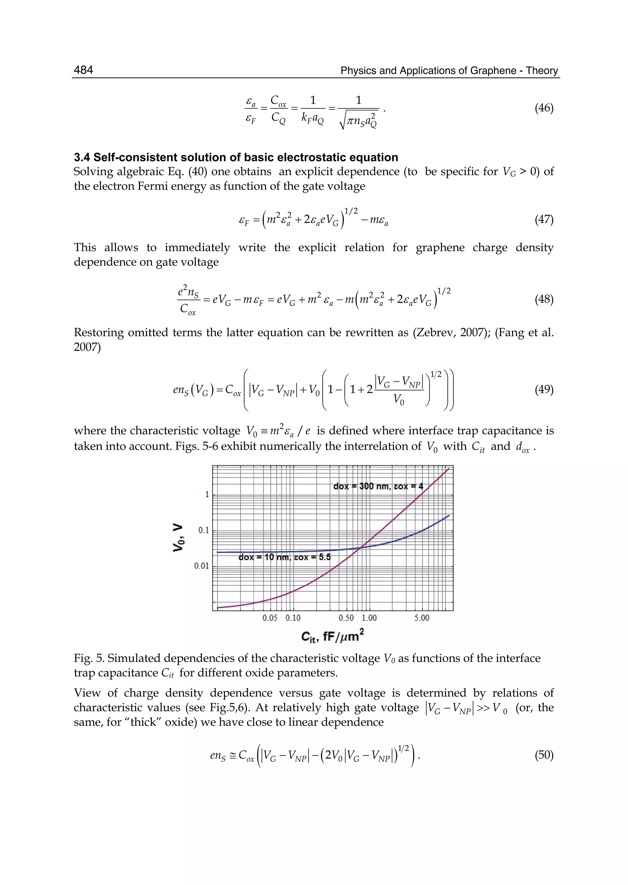
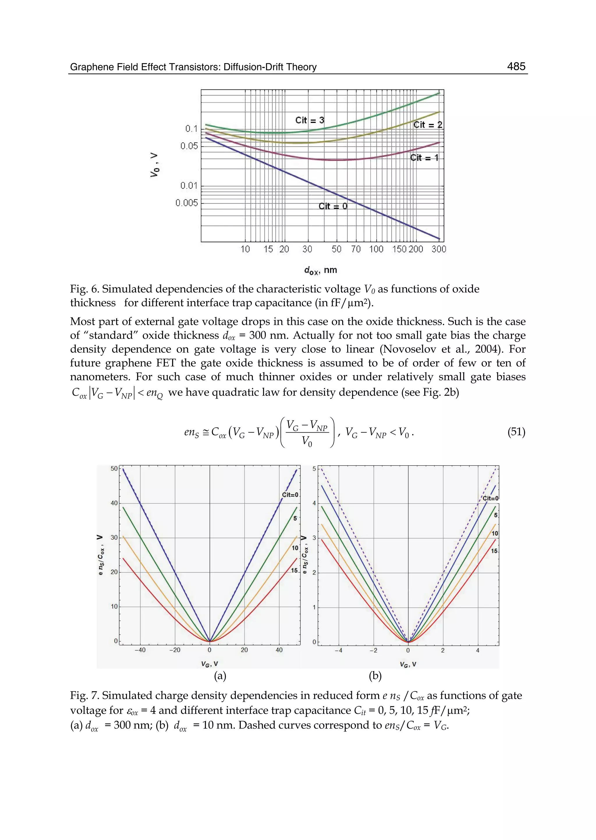
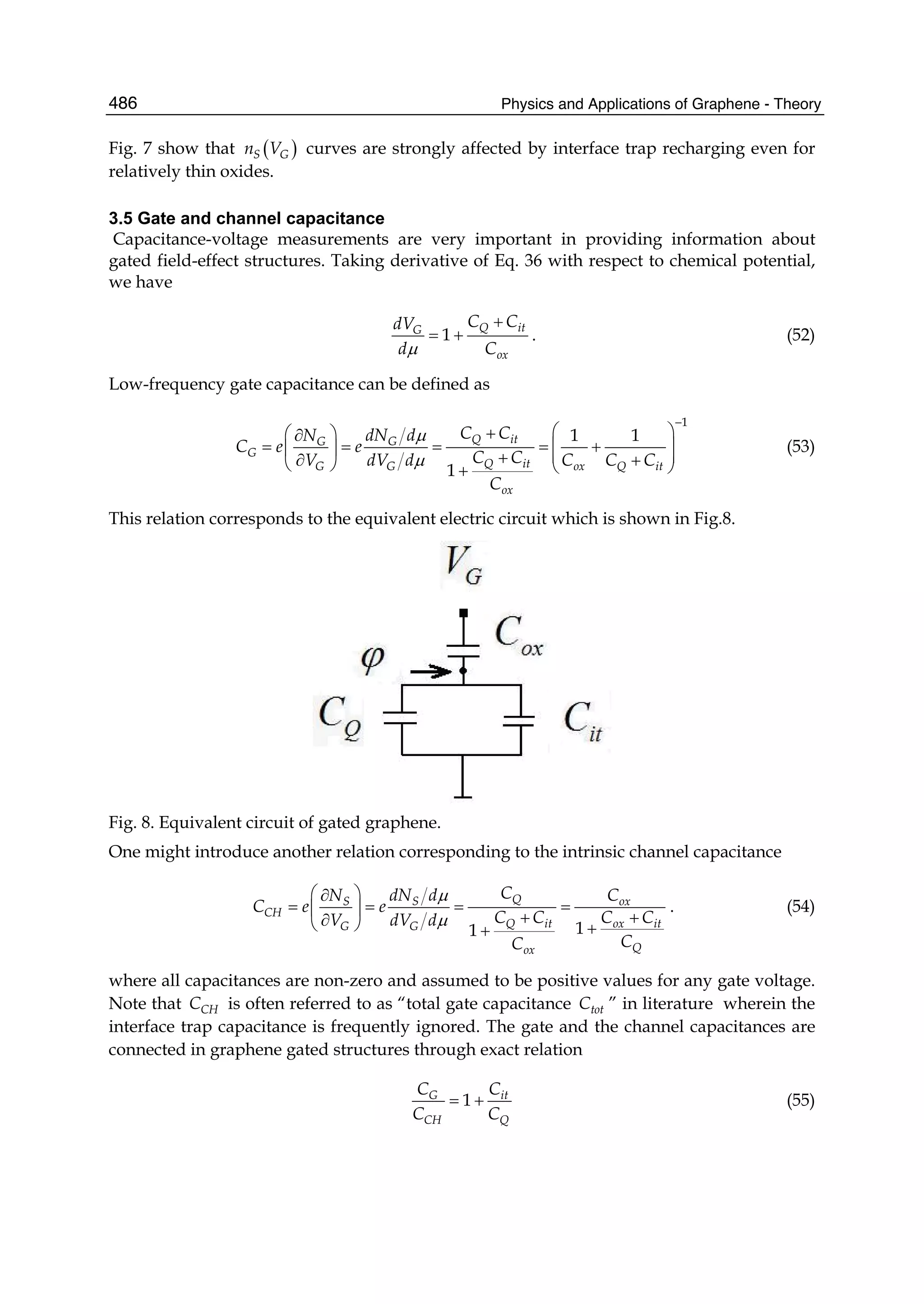
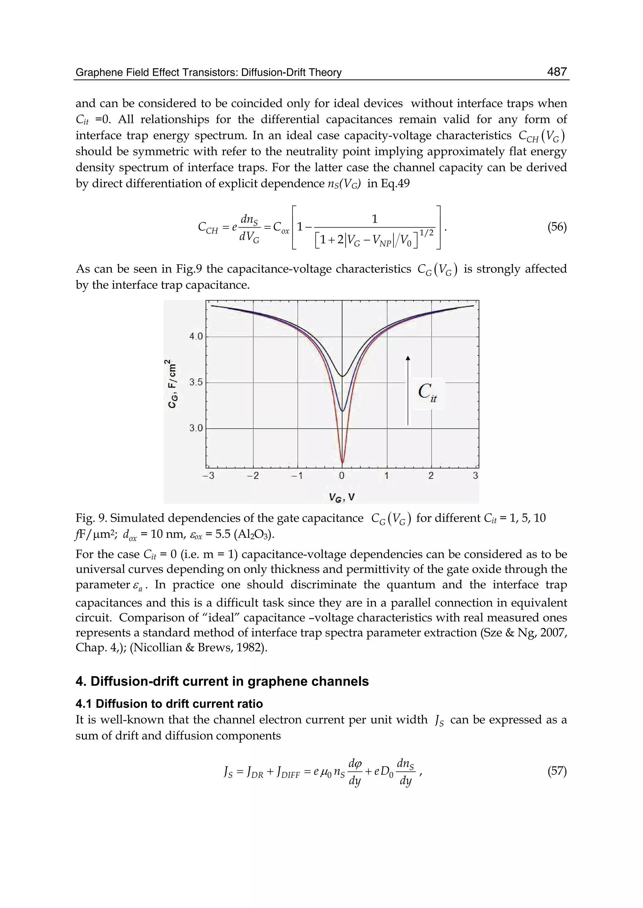
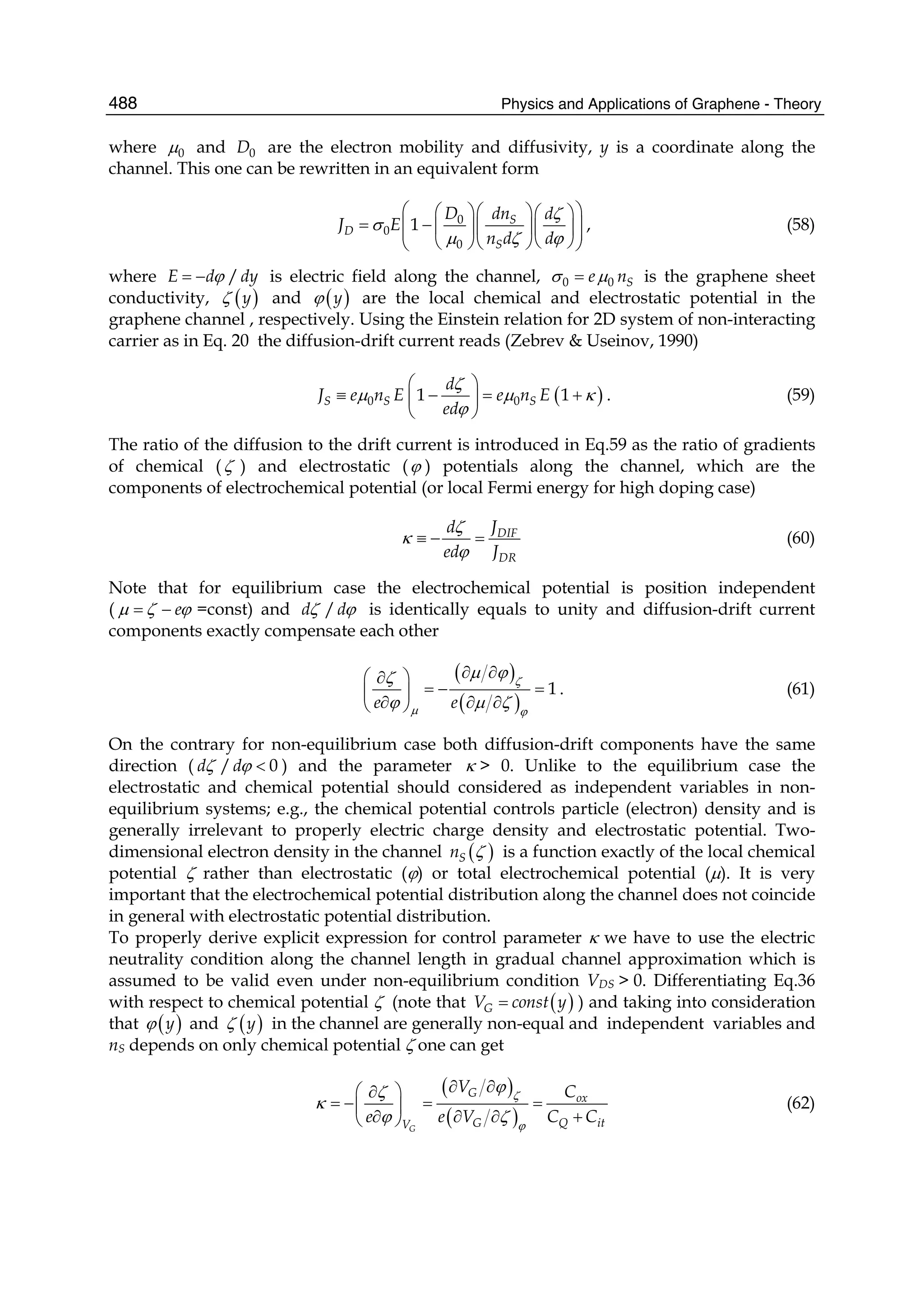
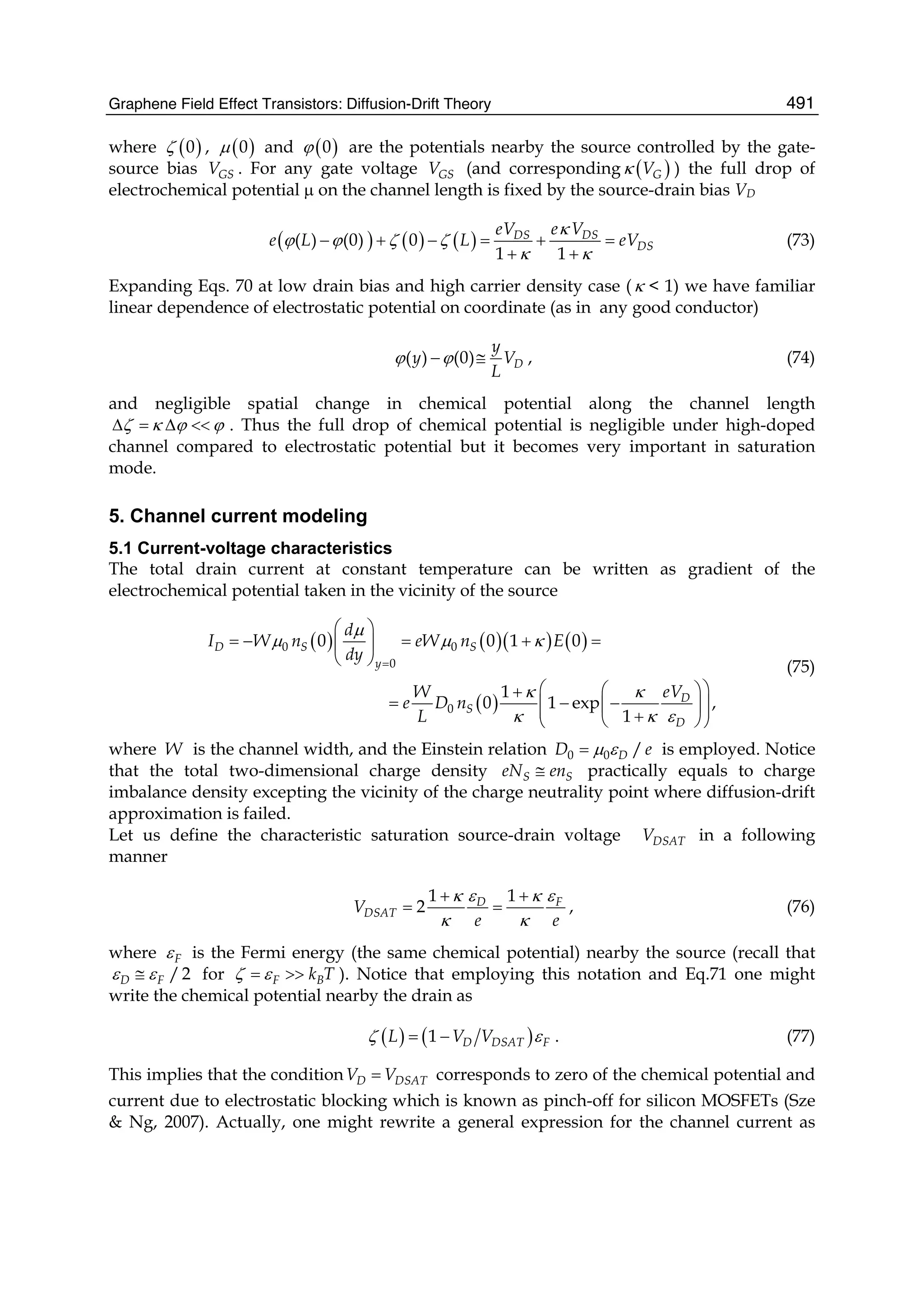
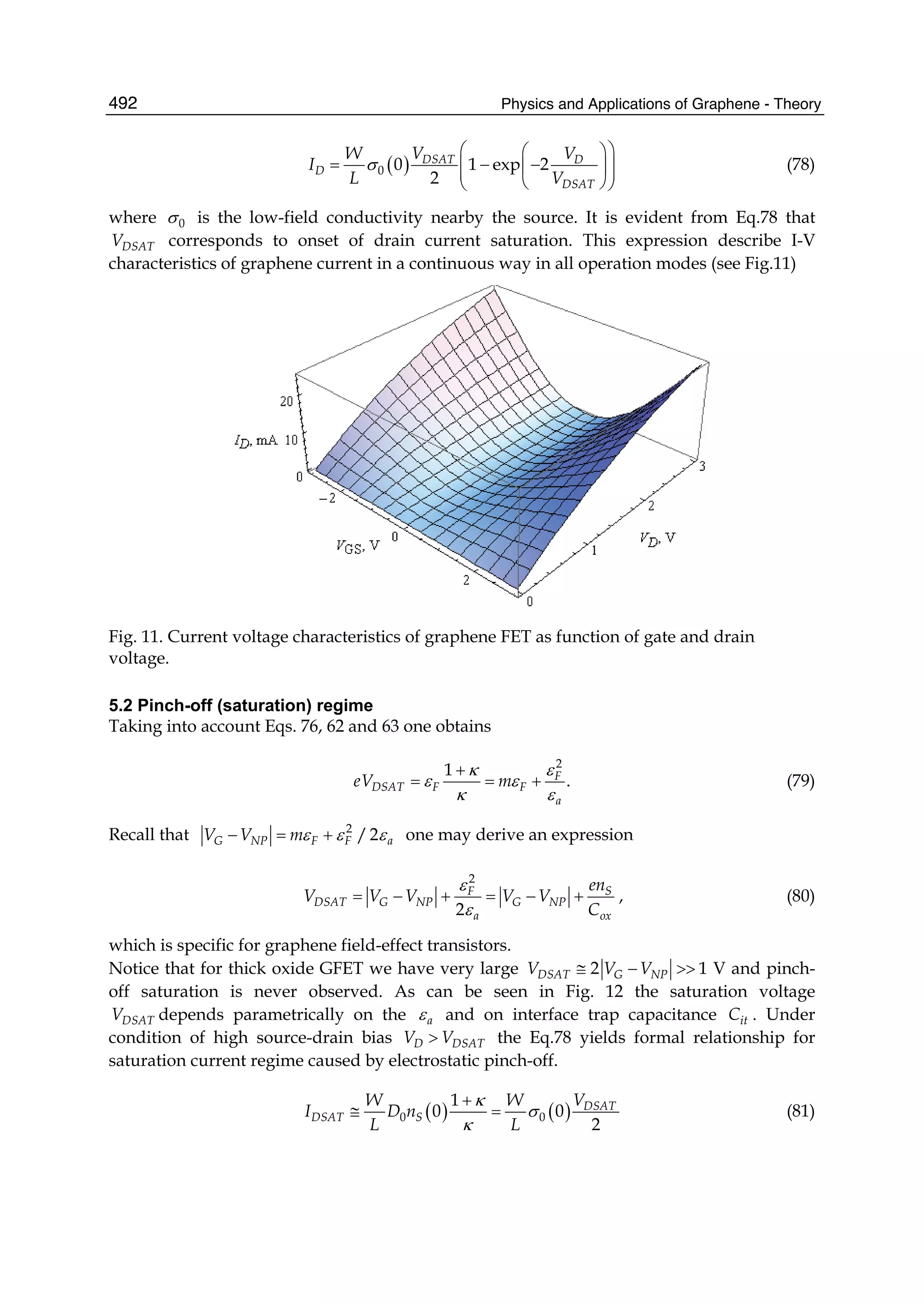
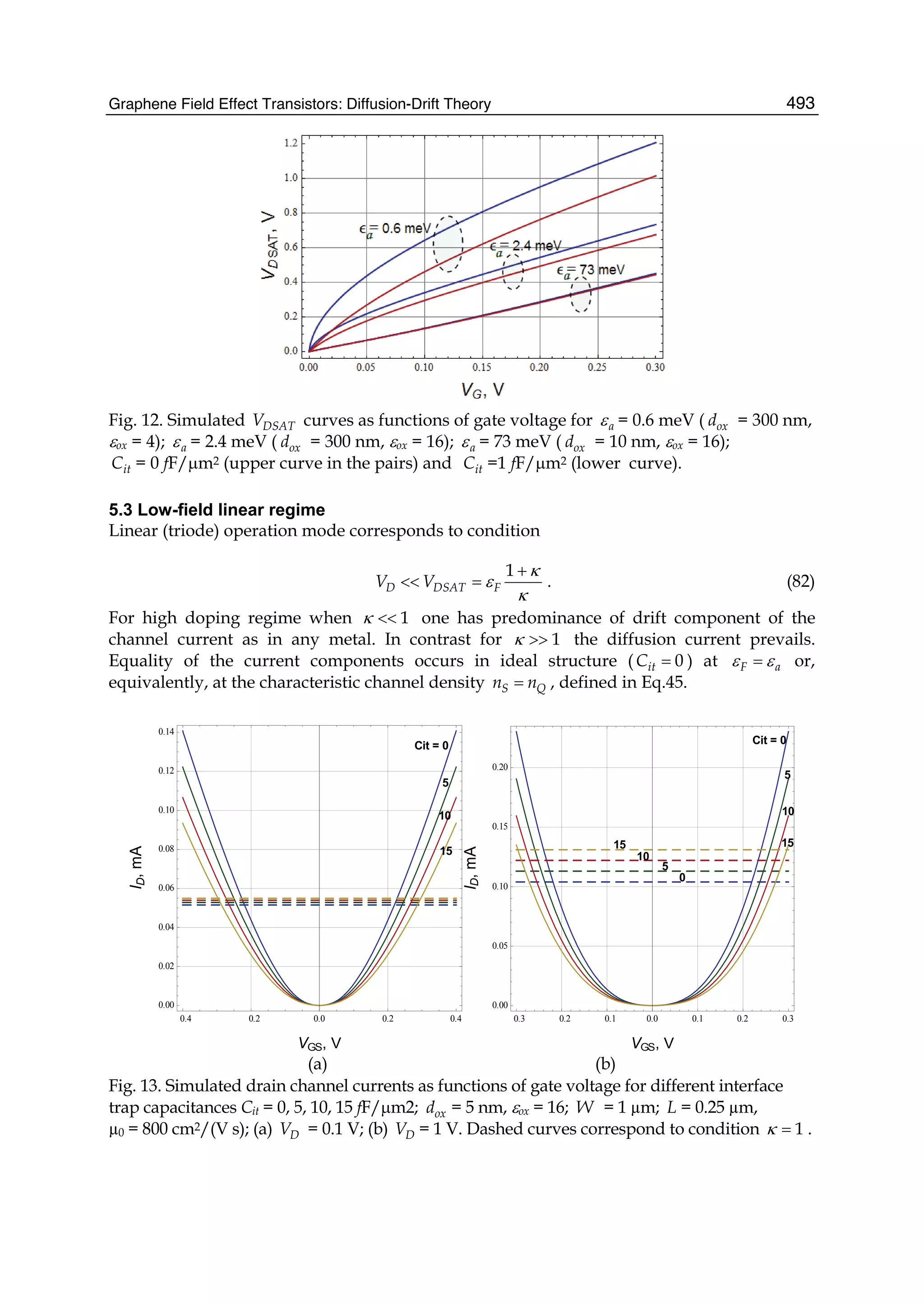

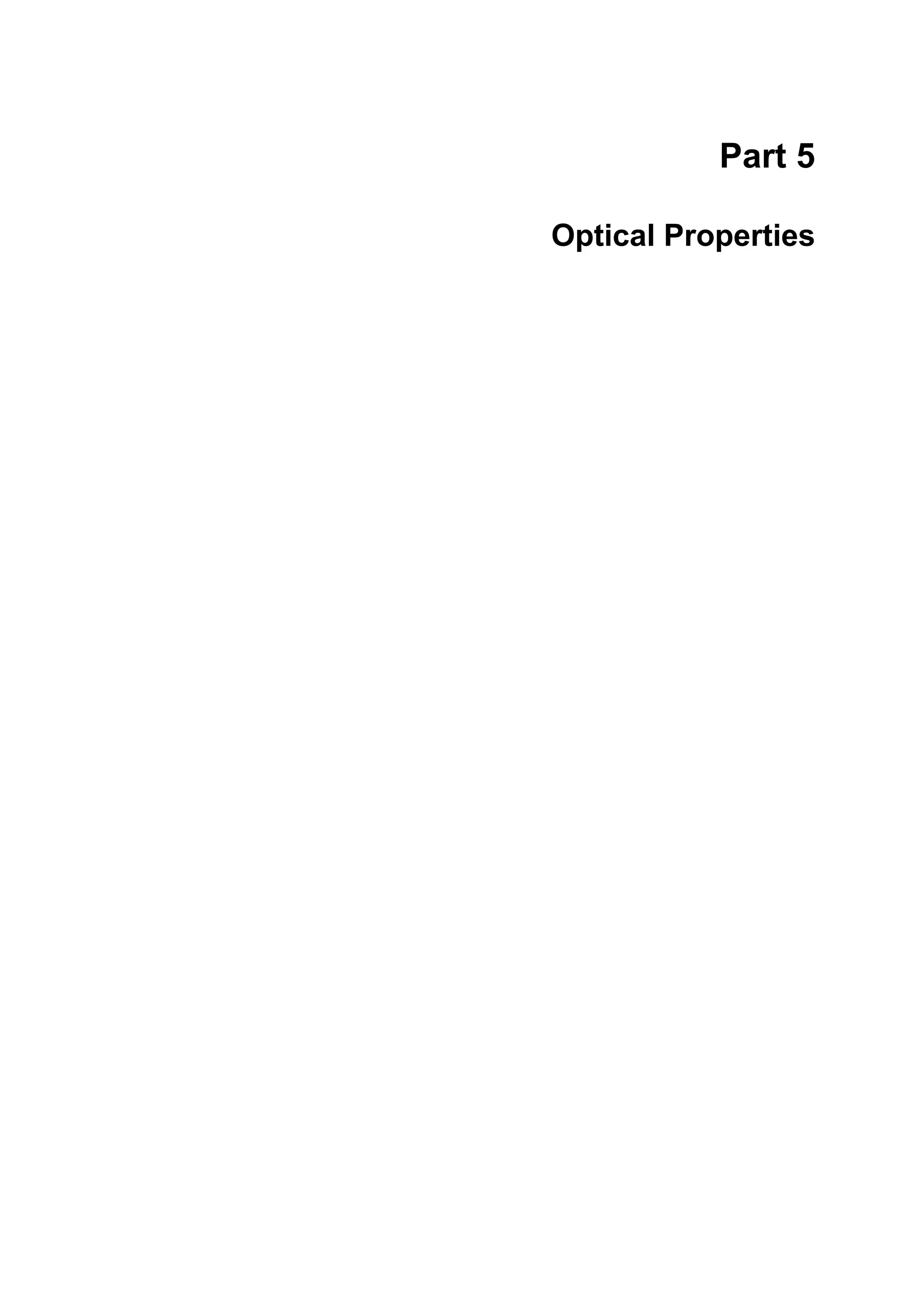

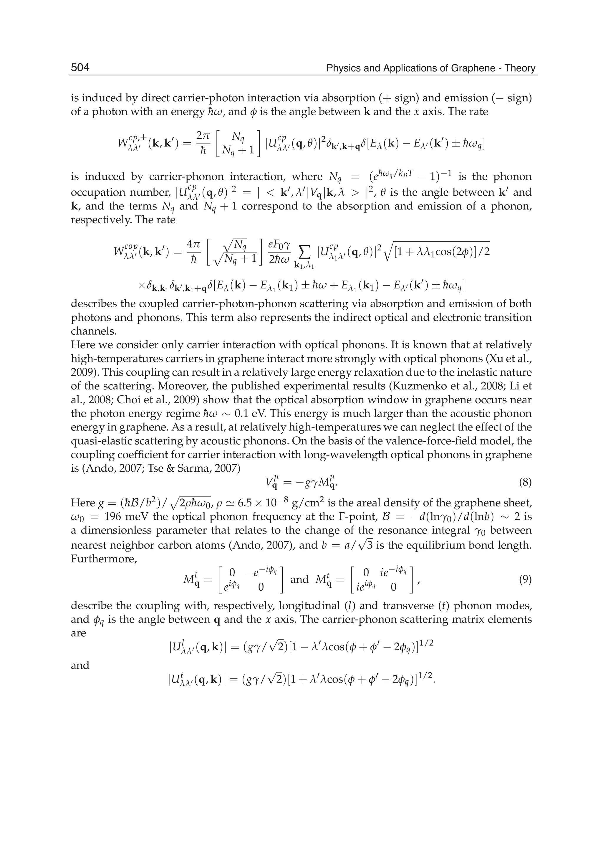
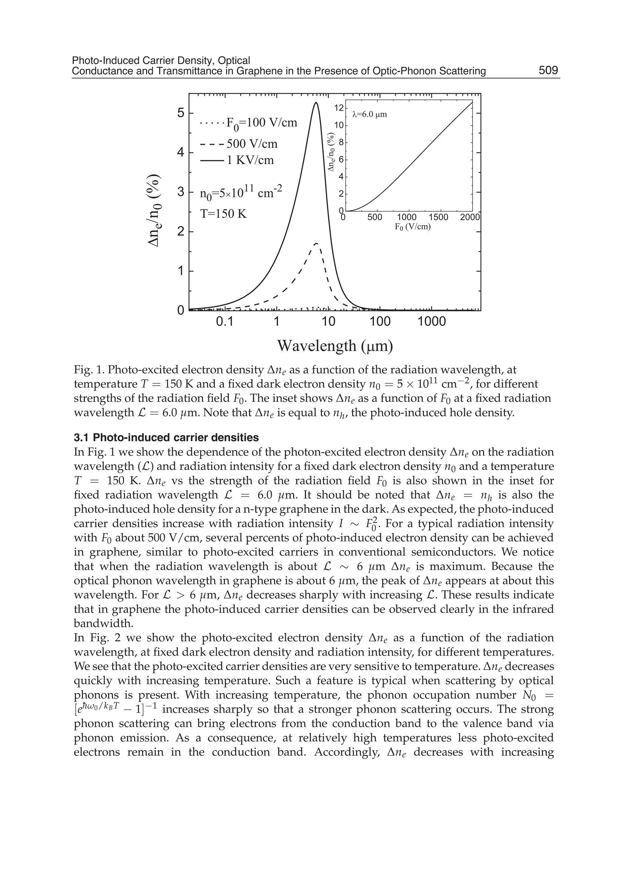
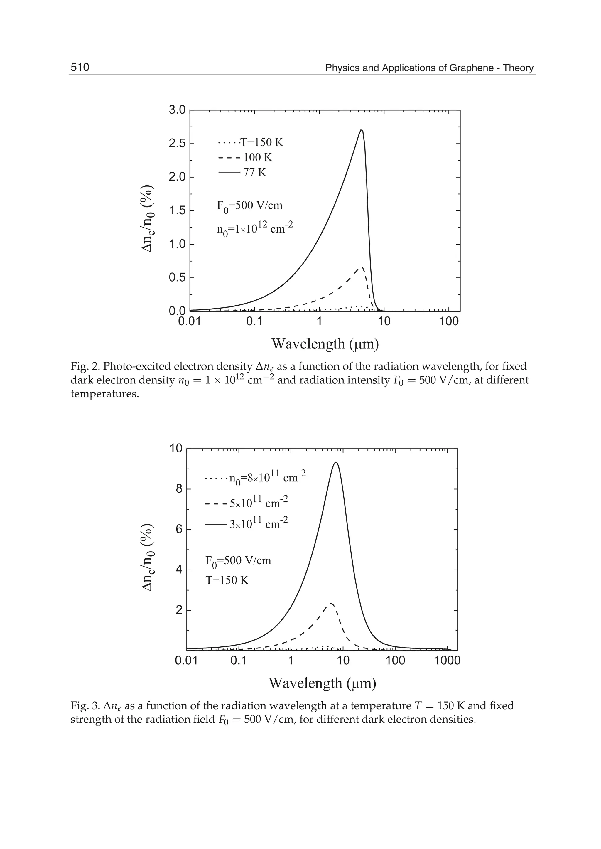
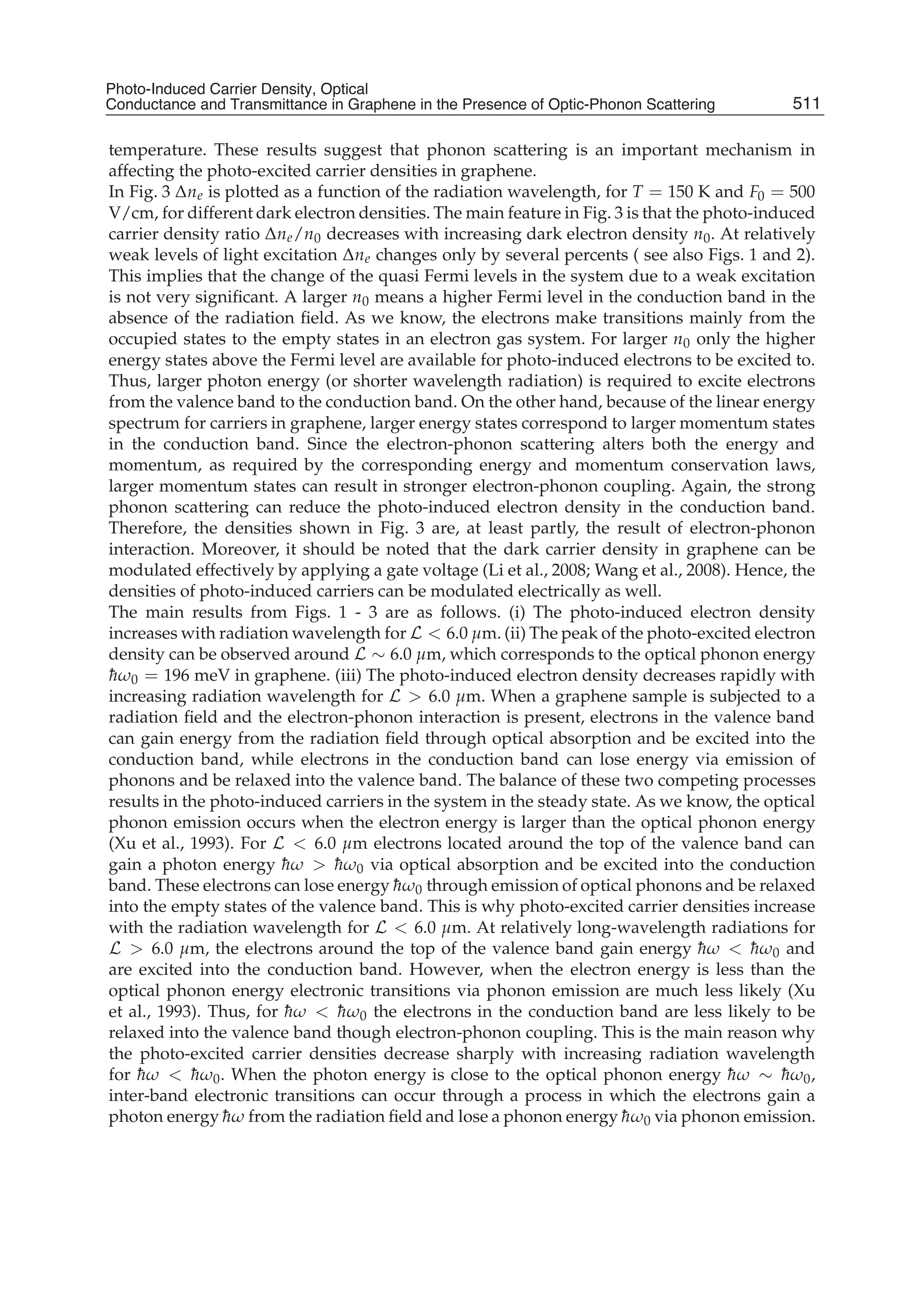
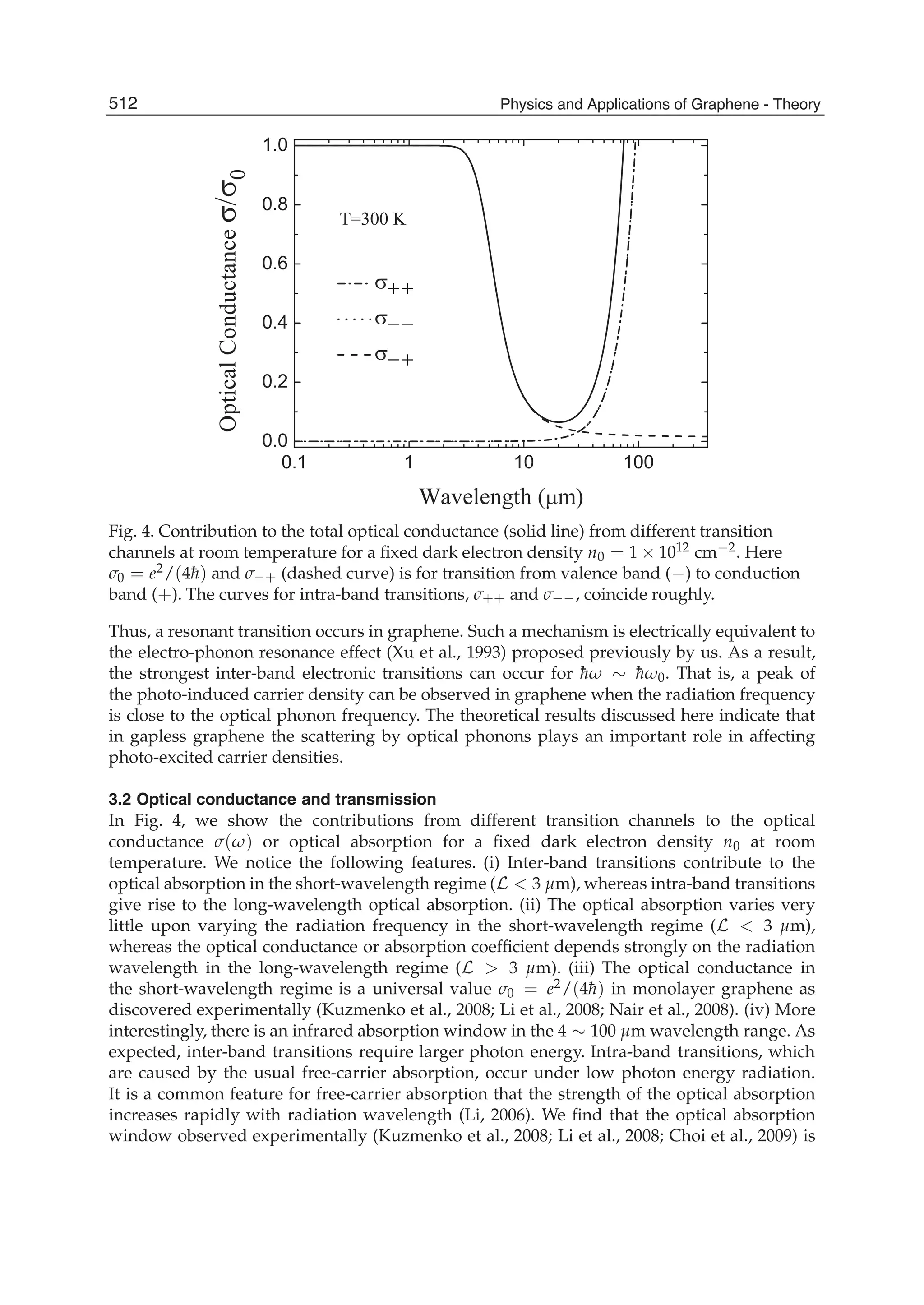
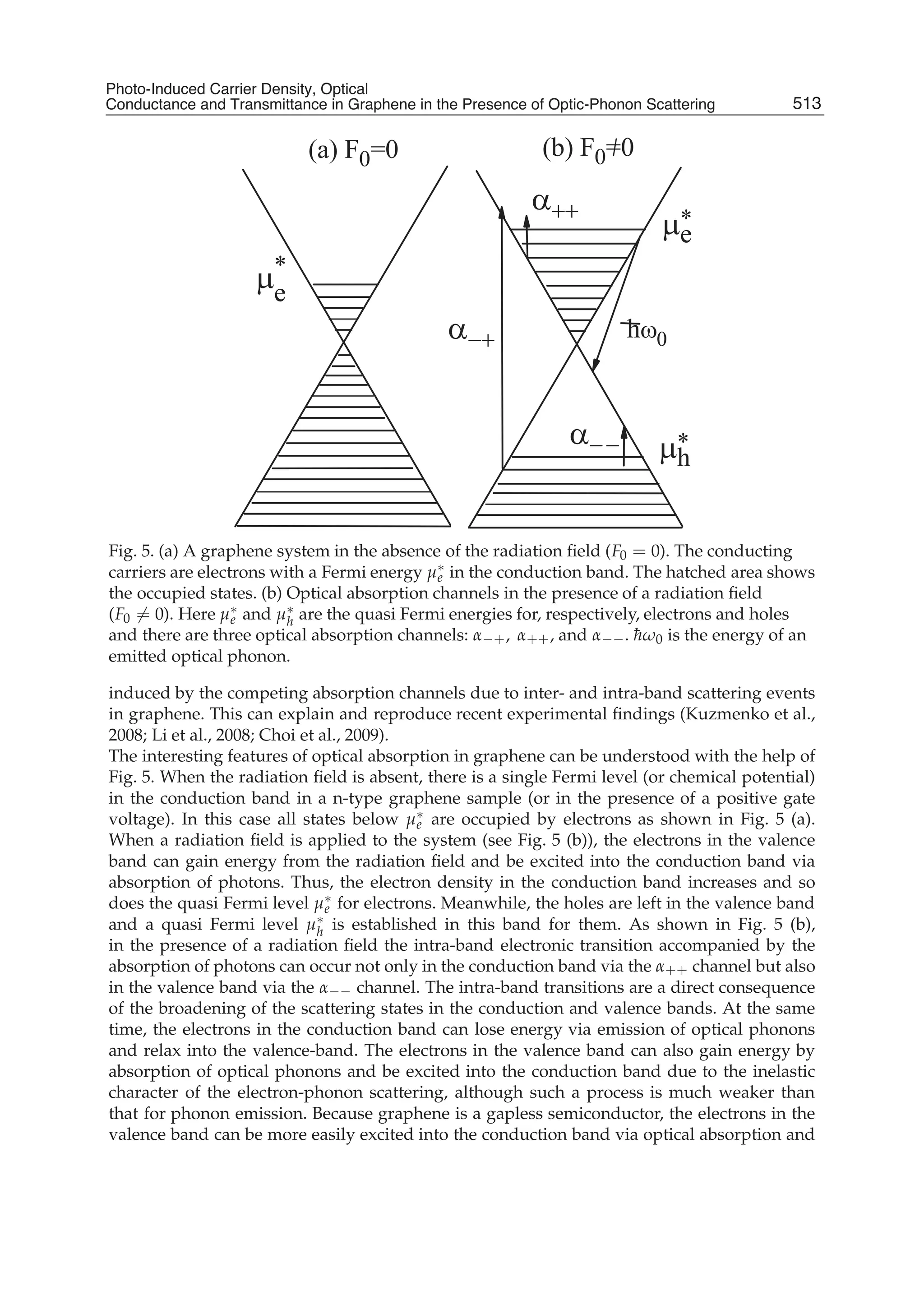
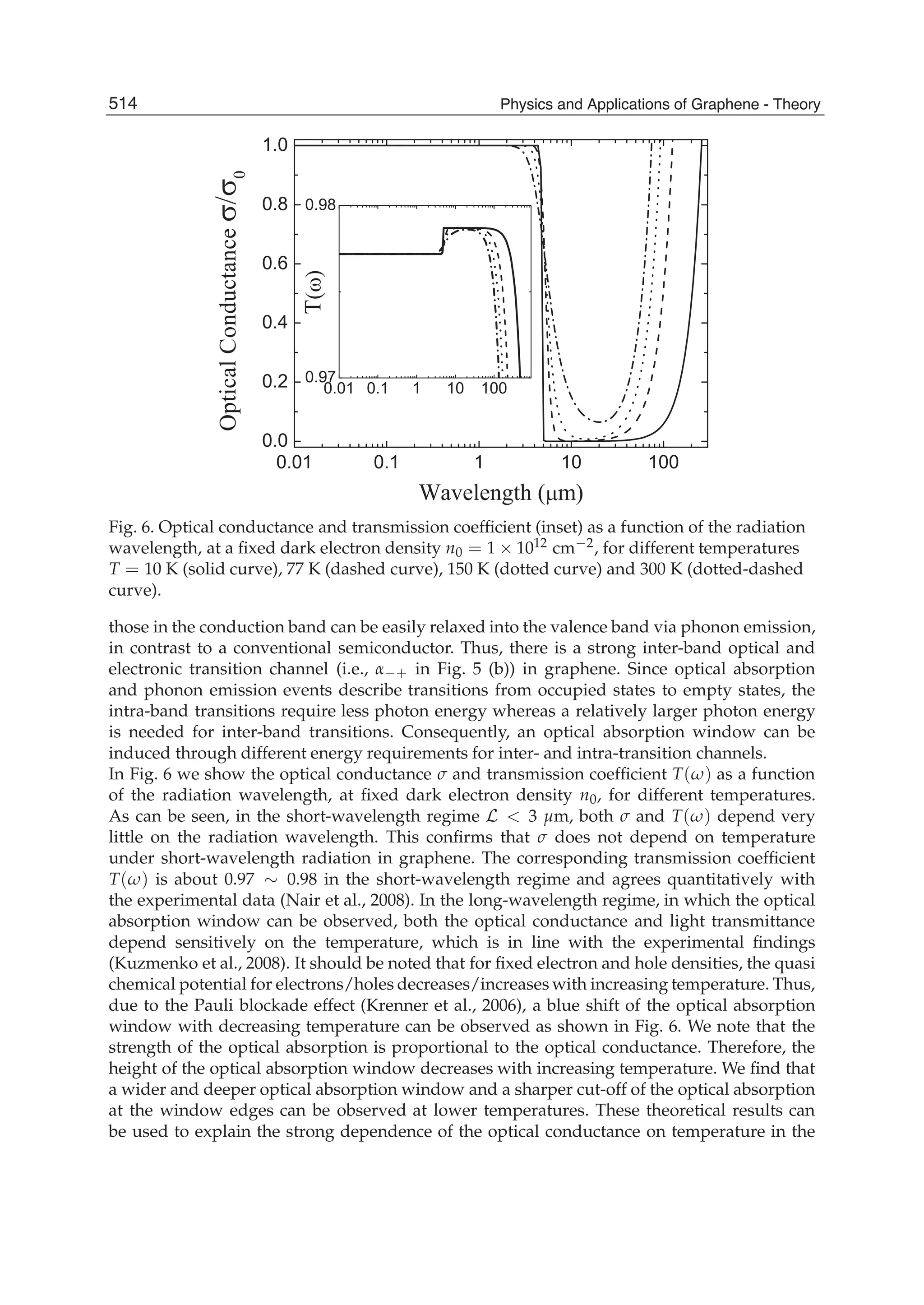
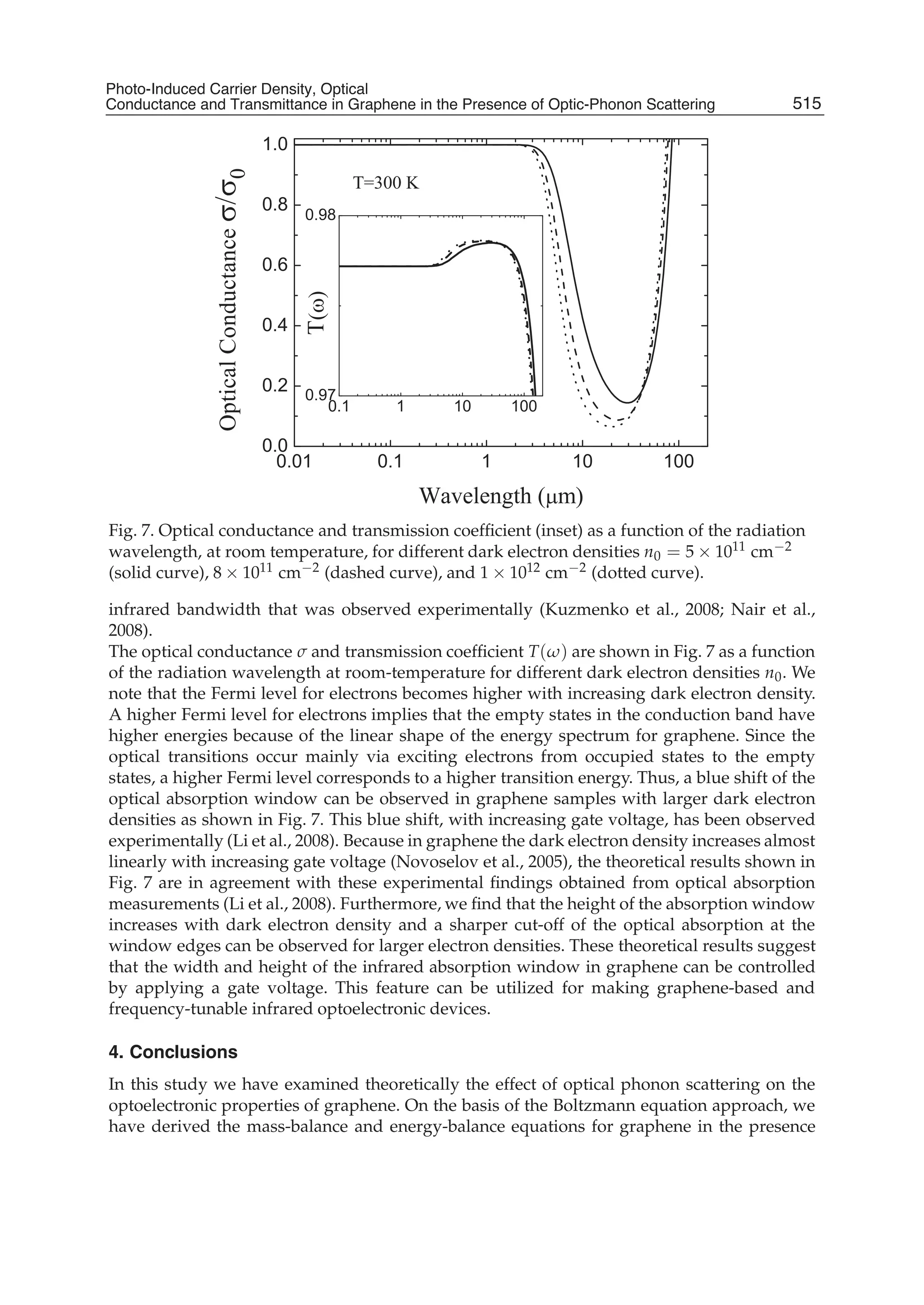
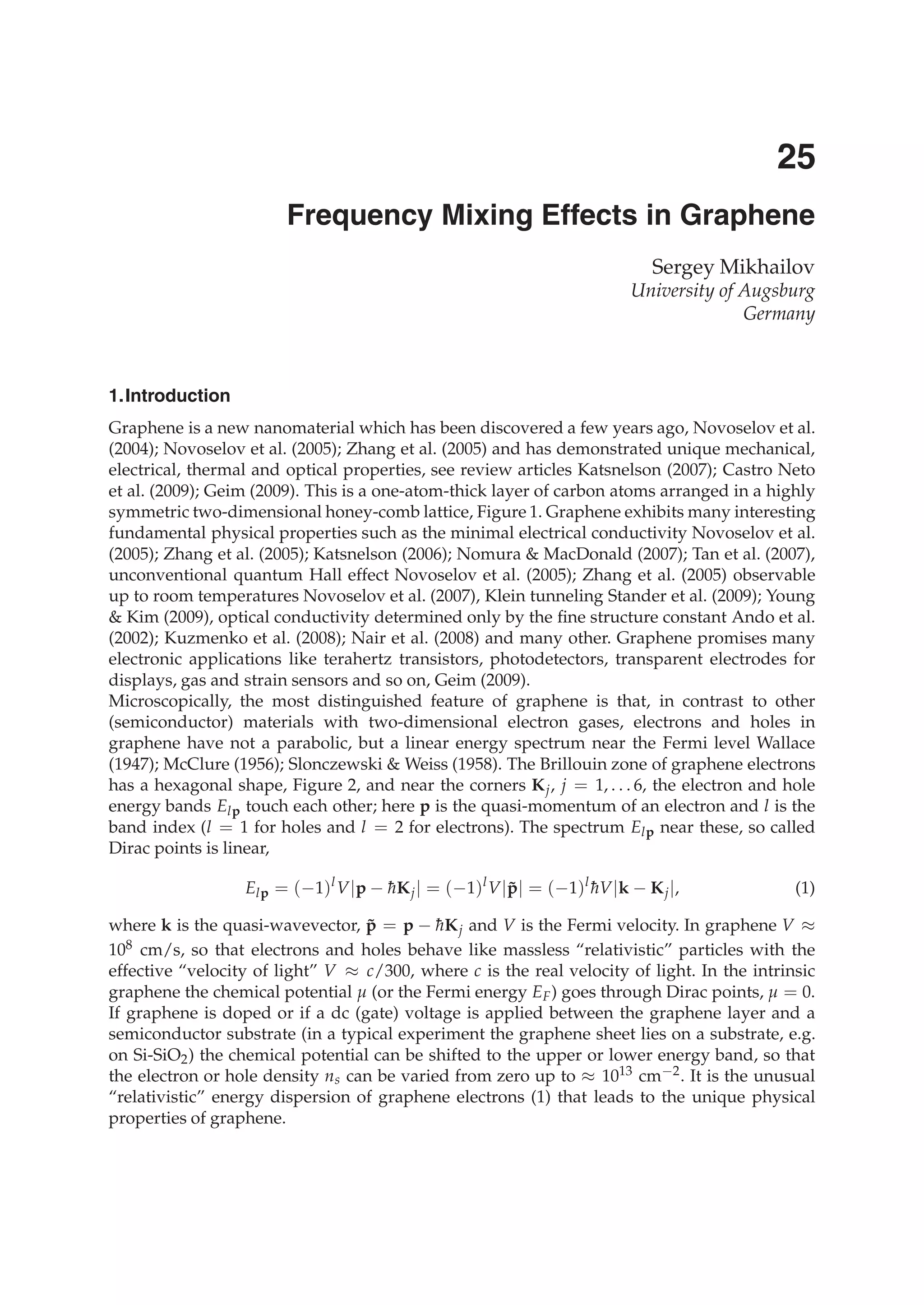
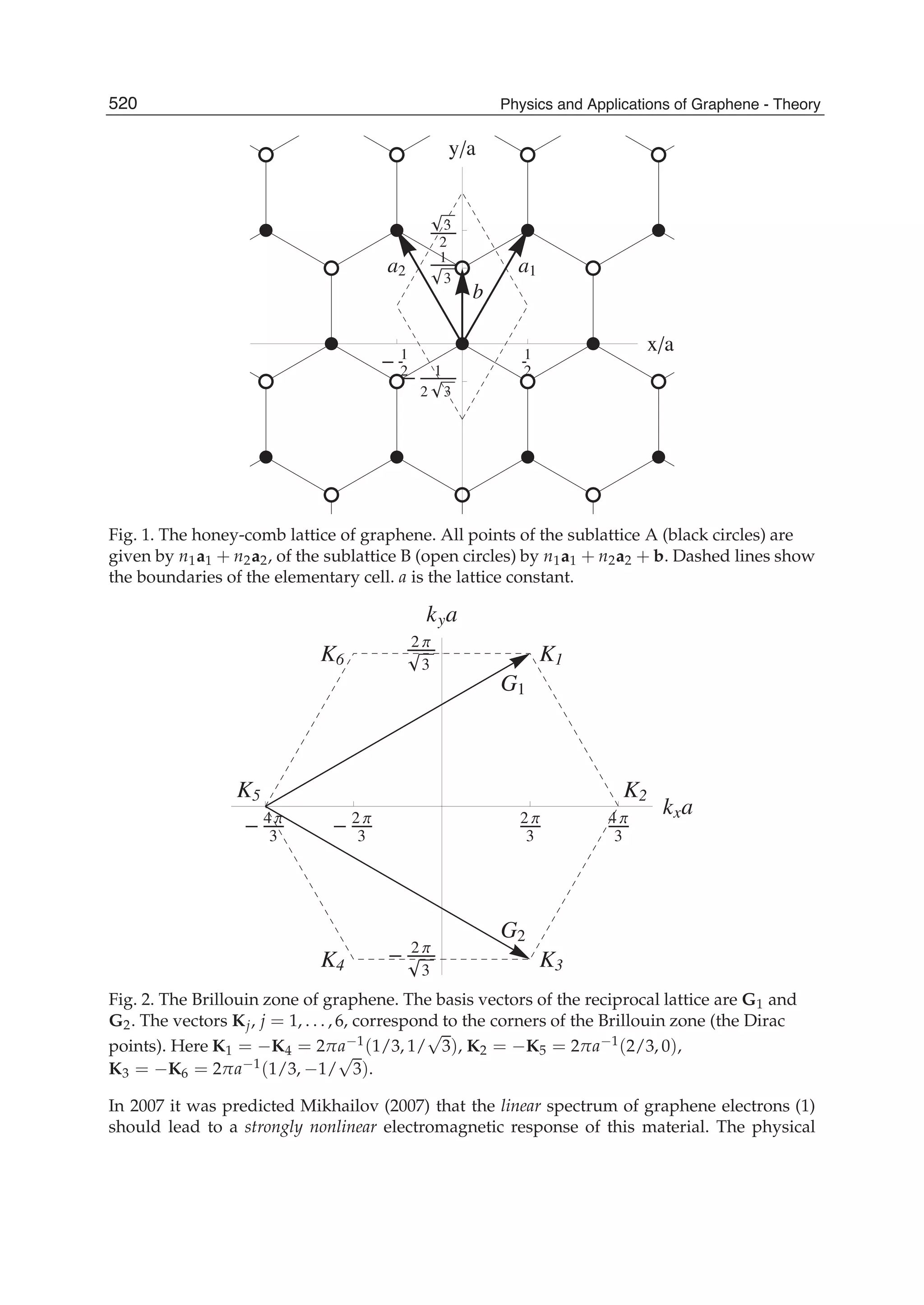
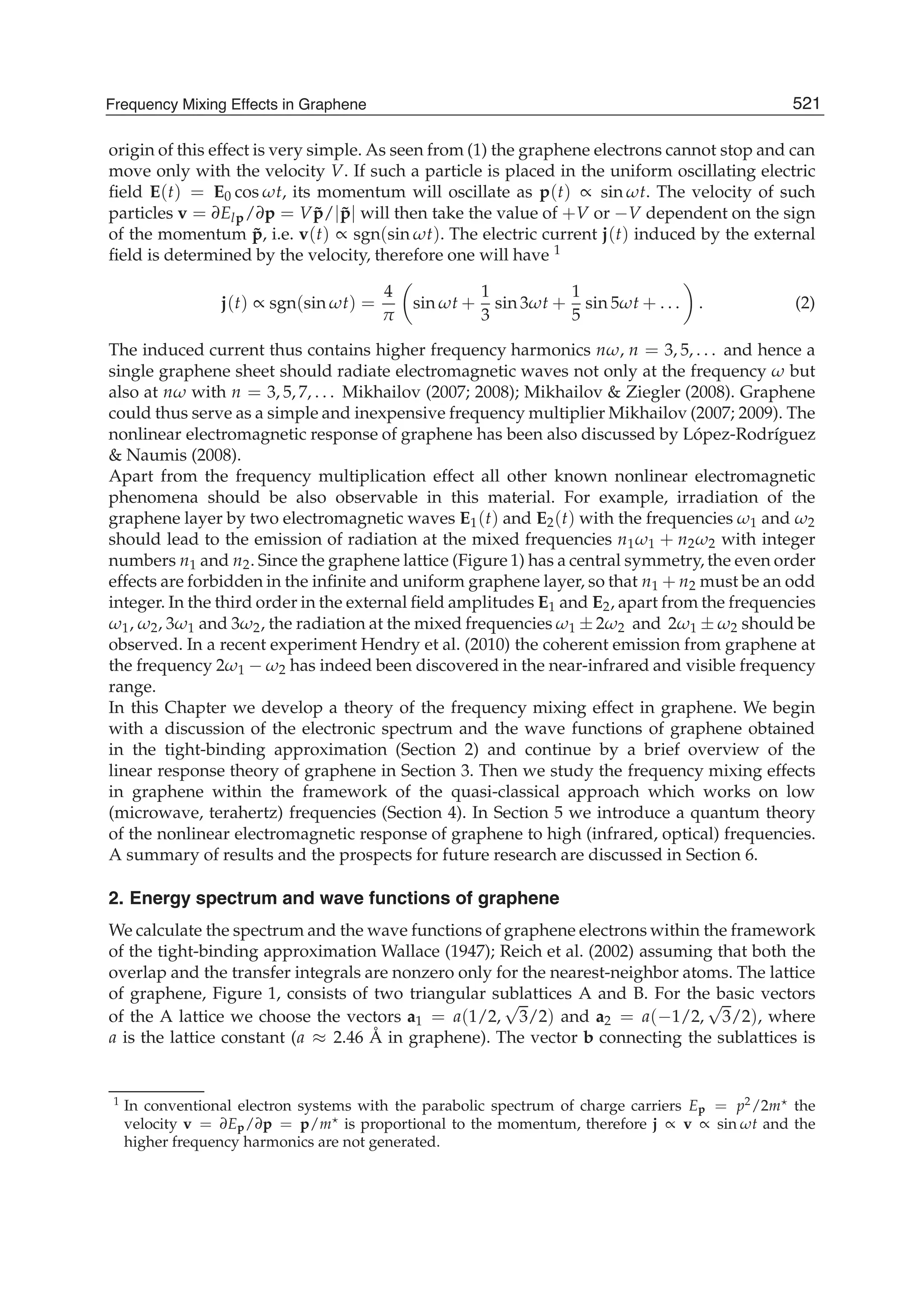
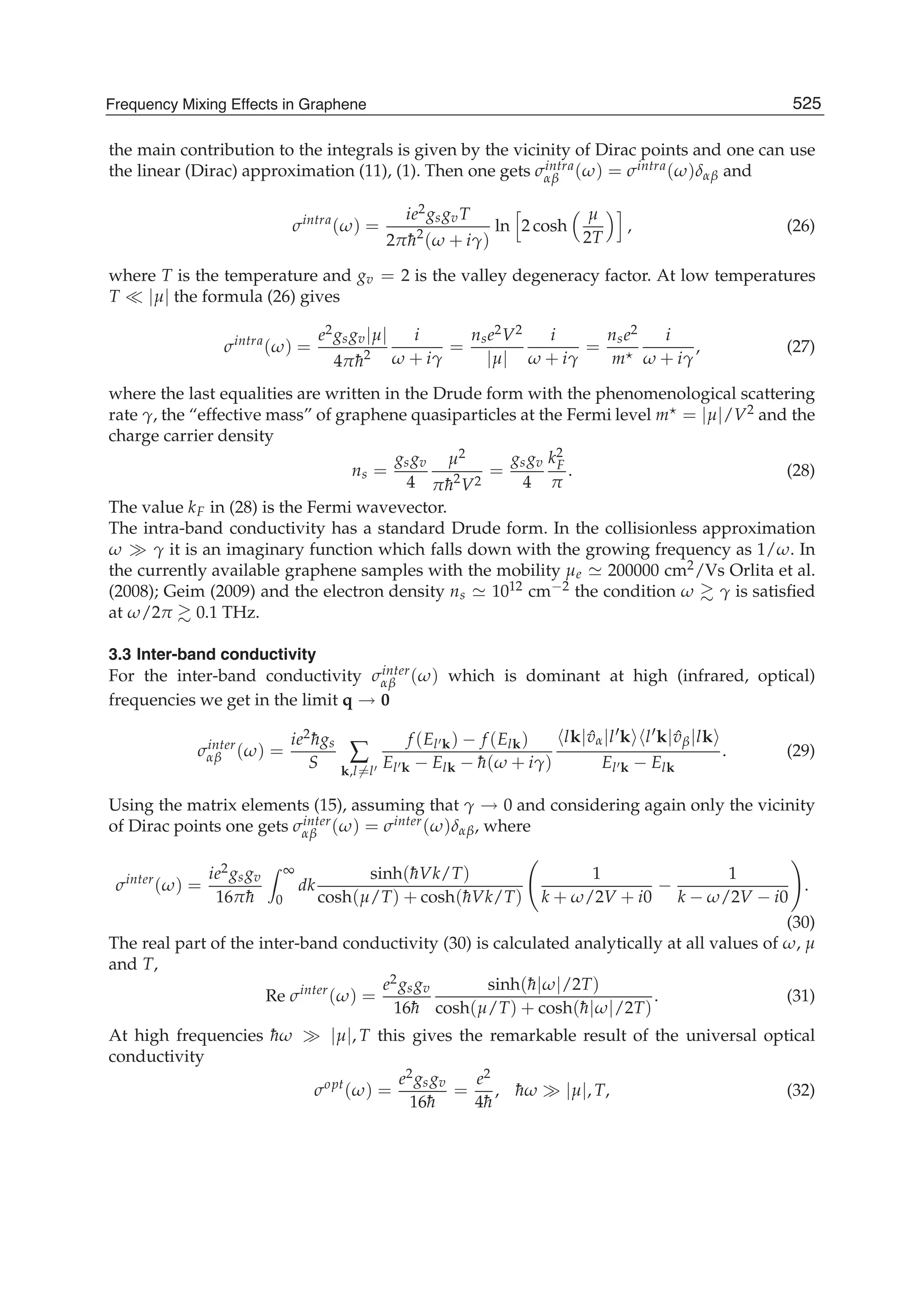
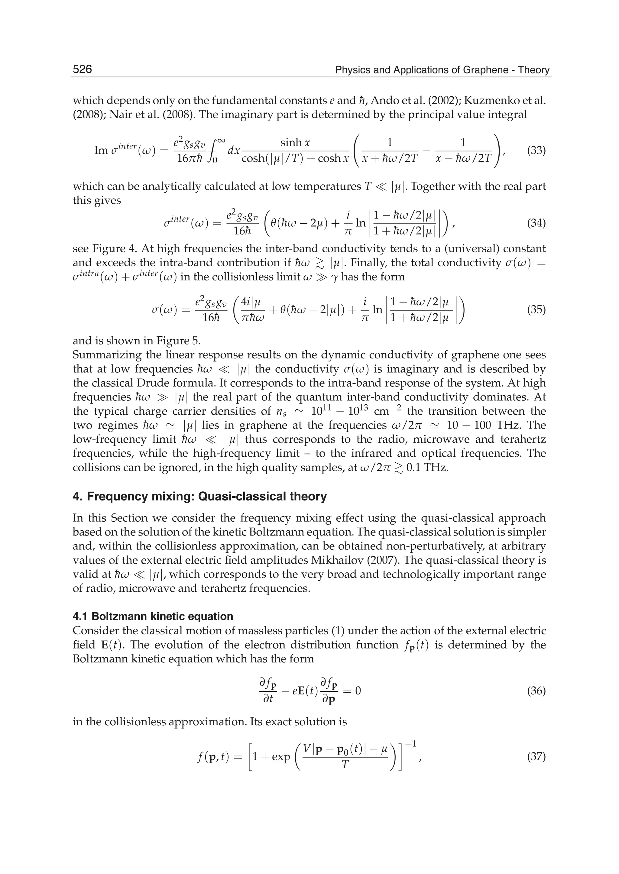

The document discusses theoretical studies on the formation, property tuning, and adsorption of graphene segments. It covers several topics: 1. Graphene synthesis methods like chemical vapor deposition (CVD) are discussed. CVD allows for large-area, high-quality graphene growth through decomposition of hydrocarbons on transition metal catalysts at high temperatures. 2. The role of hydrogen during CVD growth of carbon materials is examined. Weak van der Waals and π-π interactions between graphene sheets and how they influence properties are also studied. 3. Investigations of water clusters interacting with graphite and water encapsulated in carbon nanotubes are summarized, providing insight into confinement effects. 4


![Coded Agents – with UiPath SDK + LangGraph [Virtual Hands-on Workshop]](https://cdn.slidesharecdn.com/ss_thumbnails/codedagentsdeck-251215155422-5497c599-thumbnail.jpg?width=640&height=640&fit=bounds)


