Patterned three-color ZnCdSe/ZnCdMgSe quantum-well structures for integrated full-color and white light emitters
•
1 like•258 views

This document summarizes research on growing and characterizing patterned quantum well (QW) structures for full-color light emitting applications. Three different QWs emitting in the red, green, and yellow regions of the visible spectrum were integrated on a single indium phosphide substrate using sequential selective area epitaxy with a shadow mask. Micro-photoluminescence measurements showed well-defined excitonic emission peaks from each patterned region, demonstrating the feasibility of fabricating full-color light emitting diodes and lasers using this zinc cadmium magnesium selenide material system and growth technique.

Recommended
More Related Content
Similar to Patterned three-color ZnCdSe/ZnCdMgSe quantum-well structures for integrated full-color and white light emitters
Similar to Patterned three-color ZnCdSe/ZnCdMgSe quantum-well structures for integrated full-color and white light emitters (20)
More from Oleg Maksimov
More from Oleg Maksimov (20)
Recently uploaded
Recently uploaded (20)
Patterned three-color ZnCdSe/ZnCdMgSe quantum-well structures for integrated full-color and white light emitters
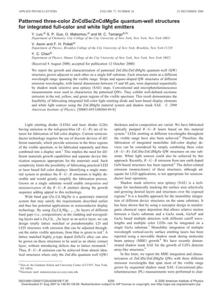
- 1. APPLIED PHYSICS LETTERS VOLUME 77, NUMBER 26 25 DECEMBER 2000 Patterned three-color ZnCdSeÕZnCdMgSe quantum-well structures for integrated full-color and white light emitters Y. Luo,a) S. P. Guo, O. Maksimov,a) and M. C. Tamargoa),b) Department of Chemistry, City College of the City University of New York, New York, New York 10031 V. Asnin and F. H. Pollaka) Department of Physics, Brooklyn College of the City University of New York, Brooklyn, New York 11210 Y. C. Chena) Department of Physics, Hunter College of the City University of New York, New York, New York 10021 ͑Received 8 August 2000; accepted for publication 12 October 2000͒ We report the growth and characterization of patterned ZnCdSe/ZnCdMgSe quantum-well ͑QW͒ structures grown adjacent to each other on a single InP substrate. Each structure emits at a different wavelength range spanning the visible range. Stripe and square-shaped QW structures of different emission wavelengths, with lateral dimensions between 15 and 60 m, were deposited sequentially by shadow mask selective area epitaxy ͑SAE͒ steps. Conventional and microphotoluminescence measurements were used to characterize the patterned QWs. They exhibit well-defined excitonic emission in the red, yellow, and green regions of the visible spectrum. This result demonstrates the feasibility of fabricating integrated full-color light emitting diode and laser-based display elements and white light sources using the ZnCdMgSe material system and shadow mask SAE. © 2000 American Institute of Physics. ͓S0003-6951͑00͒04149-8͔ Light emitting diodes ͑LEDs͒ and laser diodes ͑LDs͒ thickness and/or composition are varied. We have fabricated having emission in the red-green-blue (R – G – B) are of in- optically pumped R – G – B lasers based on this material terest for fabrication of full color displays. Current semicon- system.2 LEDs emitting at different wavelengths throughout ductor technology requires the use of discrete devices of dif- the visible range have also been achieved.4 Therefore, the ferent materials, which provide emission in the three regions fabrication of integrated monolithic full-color display de- of the visible spectrum, to be fabricated separately and then vices can be considered by simply combining three color combined into a display unit.1 This implies the need for dif- (R – G – B) ZnCdSe/ZnCdMgSe QW structures on one sub- ferent materials growth capabilities and separate device fab- strate. White light sources could also be achieved by this rication sequences appropriate for the materials used. Such approach. Recently, R – G – B emission from rare earth doped complexity limits the possibility of fabricating practical LED GaN-based structures has been reported.5 The defect-related or laser based full color displays. Identifying a single mate- emission ͑nonexcitonic͒ of those structures, although ad- rial system to produce the R – G – B emissions is highly de- equate for LED applications, is not appropriate for semicon- sirable and would greatly simplify the fabrication process. ductor laser operation. Grown on a single substrate would enable integration and Shadow mask selective area epitaxy ͑SAE͒ is a tech- miniaturization of the R – G – B emitters during the growth nique for mechanically masking the surface area selectively sequence adding appeal to this technology. and growing desired layers and structures over the exposed Wide band gap ͑Zn, Cd, Mg͒Se is a quaternary material regions.6 It is a feasible approach for the monolithic integra- system that may satisfy the requirements described earlier tion of different device structures on the same substrate. It and thus has potential applications in semiconductor display has been shown that by using a susceptor design in metalor- technology. By using Znx Cdy Mg1ϪxϪy Se layers of different ganic chemical vapor deposition that allows relative motion band gaps ͑i.e., compositions͒ as the cladding and waveguid- between a GaAs substrate and a GaAs mask, GaAsP and ing layers and a Znx Cd1Ϫx Se layer as an active layer, we can GaAs based multiple detectors with different cutoff wave- design totally lattice matched or pseudomorphic LD and lengths and multiple color LEDs can be integrated on a LED structures with emission that can be adjusted through- single GaAs substrate.7 Monolithic integration of multiple out the entire visible spectrum, from blue to green to red.2 A wavelength vertical-cavity surface emitting lasers has been lattice matched highly p-type doped ZnSeTe alloy can also reported using a moveable shadow mask during molecular be grown on these structures to be used as an ohmic contact beam epitaxy ͑MBE͒ growth.8 We have recently demon- layer, without introducing defects due to lattice mismatch.3 strated shadow mask SAE for the growth of CdTe detector Thus, R – G – B emission can be achieved from almost iden- array-like structures.9 tical structures where only the ZnCdSe quantum well ͑QW͒ In this letter, we report the MBE integration and charac- terization of ZnCdSe/ZnCdMgSe QWs with three different a͒ emission wavelengths that span most of the visible range Also at: the Graduate School and University Center of CUNY, New York, NY 10016. grown by sequential shadow mask SAE. Conventional pho- b͒ Electronic mail: tamar@scisun.sci.ccny.cuny.edu toluminescence ͑PL͒ measurements were performed to char- 0003-6951/2000/77(26)/4259/3/$17.00 4259 © 2000 American Institute of Physics Downloaded 21 Aug 2001 to 146.95.156.66. Redistribution subject to AIP license or copyright, see http://ojps.aip.org/aplo/aplcr.jsp
- 2. 4260 Appl. Phys. Lett., Vol. 77, No. 26, 25 December 2000 Luo et al. FIG. 2. ͑Color͒ Room temperature micro-PL spectra of three patterned QW regions grown on a single InP substrate. The inset is a photograph of the surface PL emission. The QWs are patterned to form three small squares each emitting at a different wavelength, one red, one yellow, and one green. shadow mask SAE for the QW integration. After the growth of the buffer layers and the flat ZnCdMgSe bottom barrier FIG. 1. ͑Color͒ ͑a͒ Schematic of the integrated ͑monolithic͒ three-color layer, the shadow mask is placed and one set of patterned quantum well structure grown. ͑b͒ Illustration of the sequential step SAE ZnCdSe QW is grown ͑i͒. The mask can then be moved process used. relative to the substrate and the second set of patterned ZnCdSe QW is deposited adjacent to the first one ͑ii͒. The acterize these patterned QW structures. Well-defined emis- third ZnCdSe QW can be grown in the same manner, after sion in the red, yellow, and green was observed from the the second one ͑iii͒. The mask can then be removed and the different patterned regions. top ZnCdMgSe barrier layer can be grown over the entire The growth was performed by shadow mask SAE in a surface. In this way, regions with different color QWs are Riber 2300P MBE system that consists of two growth cham- combined ͑i.e., integrated͒ on a single substrate. A uniform bers connected by ultrahigh vacuum ͑UHV͒ modules. One ZnSe cap layer of ϳ6 nm thick is grown to protect the chamber is dedicated to the growth of II–VI materials and ZnCdMgSe layer from oxidation. the other to III–Vs. A specially designed mask and mask Micro-PL measurements were performed to characterize fixture were used to perform this work.9 The mask fixture these integrated ZnCdSe/ZnCdMgSe patterned QWs. The allows the mask to be placed and removed from the substrate measurement was done using a triple grating micro- within the vacuum growth system so that multiple SAE steps Raman/PL spectrometer ͑JY-64000͒. The 488 nm line of an can be performed sequentially. The structures were grown on argon ion laser was used as excitation with spot size of 2–3 semi-insulating InP͑100͒ substrates that were deoxidized in m. Figure 2 shows the room temperature micro-PL spectra the III–V chamber under an As overpressure. A lattice- obtained from three patterned QW regions having different matched InGaAs buffer layer was grown under conventional emission wavelengths. The peaks are centered at around 544, MBE growth conditions to improve surface morphology. 585, and 628 nm with full widths at half maxima of 24, 19, The sample was then transferred to the II–VI chamber in and 29 nm, respectively. The relative intensities from the UHV, where a ϳ10 nm ZnCdSe low-temperature ͑LT͒ three QWs are similar, indicating that the QWs are of com- buffer layer was grown at 170 °C.10 The Zn and Cd fluxes parable quality. This implies that the quality of the QW re- had previously been adjusted to calibrate the composition of gion grown first does not degrade during the growth inter- the ZnCdMgSe and ZnCdSe layers so that they were lattice ruption, the multiple mask replacements and the deposition matched to the InP substrate and had the desired band gap. steps needed to grow the other two QWs. The variation in The ZnCdSe LT buffer layer was followed by a 0.5-m- linewidth of the three regions is consistent with the different thick ZnMgCdSe barrier layer grown at 250 °C with a band QW layer properties. The broader emission line is obtained gap of 2.8 eV. The three patterned ZnCdSe/ZnCdMgSe QWs from the red QW, which is highly strained and possibly par- were then grown sequentially on the different areas of the tially relaxed. By adjusting the ZnCdSe composition and the barrier layer using the multiple-step SAE process described thickness, a pseudomorphic QW can be designed for emis- later. Two ZnCdSe QWs, nominally 2 and 6 nm, were grown sion at this wavelength.11 The other two QWs are lattice lattice-matched to InP to produce emission in the blue and matched and thus have narrower linewidths. Of the two, the green regions. The third QW, nominally 10 nm thick, was yellow QW is the thicker one, which results in a narrower grown with a higher Cd concentration (⌬a/a of ϳ1.8% to emission spectrum due to the reduced effect of thickness InP͒ in order to obtain red emission. A schematic of the full fluctuations and interface roughness. Based on the PL emis- structure grown is shown in Fig. 1͑a͒. sion wavelengths obtained we conclude that the actual QW Figure 1͑b͒ illustrates the application of sequential thickness obtained were somewhat larger than intended. Blue Downloaded 21 Aug 2001 to 146.95.156.66. Redistribution subject to AIP license or copyright, see http://ojps.aip.org/aplo/aplcr.jsp
- 3. Appl. Phys. Lett., Vol. 77, No. 26, 25 December 2000 Luo et al. 4261 are present. Similar results were obtained from the other two regions. The growth of these three different ZnCdSe/ZnCdMgSe QWs on a single InP substrate illustrates the potential of this material and demonstrates the feasibility of using shadow mask SAE to fabricate integrated full color displays based on the ZnCdMgSe material system. By doping the two barrier layers ͑one n type and one p type͒ and growing a top highly p-type doped ZnSeTe contact layer, LEDs could be made from the patterned regions and units such as those shown in Fig. 2 could be fabricated into full color LED display ele- ments and white light sources. Furthermore, since R – G – B lasing has been observed from these materials, integrated full-color display elements based on semiconductor lasers can also be considered. Currently, no other semiconductor materials are available for this application. In summary, integration of patterned multicolored FIG. 3. Room temperature micro-PL spectra taken at four different positions in a patterned QW stripe. The positions are indicated schematically in the ZnCdSe/ZnCdMgSe QWs has been performed using shadow right-side inset. The left-side inset shows the relative intensities of the PL mask SAE. Patterned ZnCdSe/ZnCdMgSe QWs with differ- emission at the four positions. ent thickness and Cd compositions, which exhibit excitonic emission in the red, green, and yellow regions, have been grown on a single InP substrate. Excellent optical properties emission can be obtained by growing a thinner lattice- were obtained from the integrated patterned QW regions. matched ZnCdSe QW layer.12 These results demonstrate the potential of the ͑Zn, Cd, The inset of Fig. 2 is a photograph of the sample surface Mg͒Se material system and the use of shadow mask SAE that shows three square-shaped ZnCdSe QW patterned re- technique for integrated full-color (R – G – B) LED and gions emitting at different wavelengths, located near each laser-based display applications. other on the InP substrate. It was taken by a conventional photographic camera, observing through a microscope objec- The authors acknowledge the National Science Founda- tive for magnification, while the sample surface was exposed tion through Grant No. ECS-9707213 for support of this re- to the excitation laser ͑frequency-tripled Nd:yttrium– search. This work was performed under the auspices of the aluminum–garnet laser at 355 nm͒ in a conventional PL New York State Center for Advanced Technology ͑CAT͒ on setup, thus the color seen is the color of the PL emission. Ultrafast Photonic Materials and Applications. The authors The squares are about 50 mϫ50 m and they are separated also acknowledge support from the Center for Analysis of by ϳ500 m from each other. Each of the squares exhibits Structures and Interfaces ͑CASI͒ at City College. different emission wavelength range: one in the red, one in the yellow, and one in the green. The slightly distorted colors of the three squares ͑compared to the spectra shown in Figs. 1 K. Koga and T. Yamaguchi, Prog. Cryst. Growth Charact. 23, 127 ͑1991͒. 2 2 and 3͒ are most likely due to artifacts caused by the expo- L. Zeng, B. X. Yang, A. Cavus, W. Lin, Y. Y. Luo, M. C. Tamargo, Y. Guo, and Y. C. Chen, Appl. Phys. Lett. 72, 3136 ͑1998͒. sure of the film. 3 W. Lin, B. X. Yang, S. P. Guo, A. Elmoumni, F. Fernandez, and M. C. The lateral thickness and compositional variations of the Tamargo, Appl. Phys. Lett. 75, 2608 ͑1999͒. 4 patterned ZnCdSe/ZnCdMgSe QW structures were also M. C. Tamargo, W. Lin, S. P. Guo, Y. Luo, Y. Guo, and Y. C. Chen, J. probed by micro-PL. The QW emission from a single 50 m Cryst. Growth 214Õ215, 1058 ͑2000͒. 5 A. J. Steckl and J. M. Zavada, MRS Bull. 24, 33 ͑1999͒. wide stripe was measured at several positions along the 6 A. Y. Cho and F. K. Reinhart, Appl. Phys. Lett. 56, 2304 ͑1990͒. stripe width. Figure 3 shows the results from a stripe having 7 T. Katsuyama, M. A. Tischler, D. J. Moore, and S. M. Bedair, J. Cryst. emission at 585 nm. The inset shows the positions within the Growth 77, 85 ͑1986͒. 8 H. Saito, I. Ogura, Y. Sugimoto, and K. Kasahara, Appl. Phys. Lett. 66, stripe in which the measurements were taken. Identical spec- 2466 ͑1995͒. tra are observed in the different positions indicating good 9 Y. Luo, L. Zeng, W. Lin, B. Yang, M. C. Tamargo, Y. M. Strzhemechny, uniformity of the QW thickness and composition within the and S. A. Schwarz, J. Electron. Mater. 29, 598 ͑2000͒. 10 patterned region. The spectrum taken exactly at the edge of L. Zeng, B. X. Yang, M. C. Tamargo, E. Snoeks, and L. Zhao, Appl. Phys. Lett. 72, 1317 ͑1998͒. the stripe ͑plot No. 4͒ shows a reduced intensity. However, 11 L. Zeng, Ph.D. dissertation, The City College of CUNY, New York, 1998. the peak position is unchanged and no other emission peaks 12 A. Cavus, L. Zeng, M. C. Tamargo, N. Bamba, F. Semendy, and A. Gray, are observed, an indication that no deleterious edge effects Appl. Phys. Lett. 68, 3446 ͑1996͒. Downloaded 21 Aug 2001 to 146.95.156.66. Redistribution subject to AIP license or copyright, see http://ojps.aip.org/aplo/aplcr.jsp