The paper proposes a new structure for heterojunction quantum dot solar cells (HJQD SC) to enhance efficiency and reduce material usage by employing quantum dot layers instead of traditional bulk structures. The theoretical analysis demonstrates improved optical and electrical characteristics, allowing for better energy conversion while maintaining lower costs. Various models and parameters are compared, emphasizing the importance of quantum dot sizes in optimizing solar cell performance.
![International Journal of Electrical and Computer Engineering (IJECE)
Vol. 10, No. 3, June 2020, pp. 2918~2925
ISSN: 2088-8708, DOI: 10.11591/ijece.v10i3.pp2918-2925 2918
Journal homepage: http://ijece.iaescore.com/index.php/IJECE
Design modern structure for heterojunction quantum
dot solar cells
A. Thabet1
, S. Abdelhady2
, Youssef Mobarak3
1
Electrical Engineering Department, College of Engineering, Qassim University, Kingdom of Saudi Arabia
3
Electrical Engineering Department, Faculty of Engineering, King Abdulaziz University, Kingdom of Saudi Arabia
1,2,3
Nanotechnology Research Center, Faculty of Energy Engineering, Aswan University, Egypt
Article Info ABSTRACT
Article history:
Received Mar 25, 2019
Revised Dec 5, 2019
Accepted Dec 13, 2019
This paper proposal new structure for improving the optical, electrical
characteristics and efficiency of 3rd
generation heterojunction quantum dot
solar cell (HJQDSC) (ITO/CdS/QDPbS/Au) model by using the quantum dot
window layer instead of bulk structure layers cell. Also, this paper presents
theoretically analysis for the performance of the proposal HJQDSC
(ITO/QDCdS/QDPbS/Au) structure. The new design structure was applied
on traditional (SnO2/CdS/CdTe/Cu) and (ZnO/CdS/CIGS/Mo) thin film solar
cells which based on sub-micro absorber layer thickness models by replacing
the bulk CdTe, CIGS absorber layers and CdS window layer with quantum
dot size materials to achieve higher efficiency with lesser usage layer
material. Also, it has been studied the effect of using semiconductors layers
in quantum dots size on electric and optical properties of thin film solar cells
and the effect of window and absorber layers quantum dots radii on
the performance of solar cells. Finally, a thermal efficiency analysis has been
investigated for explaining the importance of new structure HJQD solar cells.
Keywords:
Absorber
Energy conversion
Heterojunction
Quantum dot
Solar cell
Copyright © 2020 Institute of Advanced Engineering and Science.
All rights reserved.
Corresponding Author:
Safaa Abdelhady,
Department of Electrical Engineering,
Aswan University,
Sahary Road, Aswan 81528, Egypt.
Email: engsafaa33@gmail.com
1. INTRODUCTION
Several solar technologies including wafer, thin film and organic, have been researched to achieve
reliability, cost-effectiveness and high efficiency. Cost effectiveness can be seen in the use of less material as
well as increasing energy conversion efficiency. The reduction in the efficiencies of the previous models due
to the reduction of absorber layers thickness are associated with a number of problems [1-3].
The 3rd
generation of solar cells technique based on novel absorber layer materials with tunable bandgap that
can be tuned to match the spectral distribution of solar spectrum are crucial and achieved less consummation
absorber layer material. Quantum dots have the merit of tunable bandgap as a result of size variation as well
as formation of intermediate bands. The energy band gap increases with a decrease in size of the quantum
dot, the adjustable bandgap of quantum dots allows the construction of nanostructured solar cell that is able
to harvest more of the solar spectrum [4]. Quantum dots can generate multiple exciton (electron-hole pairs)
after collision with one photon of energy exceeding the band gap. Absorption of UV photons in quantum dots
produces more electrons than near infrared photons. Quantum dots emit up to three electrons per photon due
to multiple exciton generation as opposed to only one for standard crystalline silicon solar cell [5].
The previous study for heterojunction solar cells based on PbS-QDs/CdS thin films demonstrating
an achieved efficiency of 3.3% [6].](https://image.slidesharecdn.com/v1413dec5dec25mar19781f-201210021708/75/Design-modern-structure-for-heterojunction-quantum-dot-solar-cells-1-2048.jpg)
![Int J Elec & Comp Eng ISSN: 2088-8708
Design modern structure for heterojunction quantum dot solar cells (A. Thabet)
2919
This paper proposal new structure for previous heterojunction quantum dot ITO/CdS/QDPbS/Au
thin film solar cell model to improve the efficiency of the model by using the quantum dot absorber layer and
replaced the bulk CdS window layer with quantum dot CdS layer. It has been applied the new structure
model on the previous SnO2/CdS/CdTe/Cu and ZnO/CdS/CIGS/Mo thin film models which based on
sub-micro absorber layer thickness to improve the performance and efficiency of the cells to save
the consumption in the absorber layer material. The effect of window and absorber layers’ quantum dots radii
on the performance of the selected cells. A comparative study is done for specifying the best size of window
and absorber layer materials to achieve higher efficiency with lesser usage semiconductor materials and
lesser production cost and time.
2. MATHEMATICAL MODELS OF PROPOSAL HJQD THIN FILM SOLAR CELLS
Considering spherical shape of nanostructure layer material in thin film solar cell, based on
the model developed by Louis Brus for colloidal quantum dots. The energy band gap of quantum dot layer
material can be approximated by 1, and that bandgap energy values increase as the quantum dot
size decreases [7].
𝐸𝑔(𝑄𝑑𝑜𝑡𝑠) = 𝐸𝑔𝑏𝑢𝑙𝑘 +
𝜋2ℎ2
2𝑅2
(
1
𝑚 𝑒𝑏
+
1
𝑚ℎ𝑏
) −
1.8𝑄2
4𝜋𝜀 𝑏 𝜀 𝑜 𝑅
(1)
where: R is radius of quantum dot layer material, meb, mhb are the effective mass of electron and hole for
layer material, Q is the elementary charge, ε0 is the permittivity of free space, and h is Plank constant.
The energy bandgap value of the bulk layer material calculated using Varshni relation temperature
dependence of the bandgap in semiconductors which using in absorber or window layer can be
described as [8-10].
𝐸𝑔𝑏𝑢𝑙𝑘 = 𝐸𝑔(0) −
𝑇2
𝛽
(2)
where, Eg(0) is energy band gap of semiconductor material at zero temperature, and are constants, εb is
dielectric constant of the semiconductor layer material which can be described by using the Drude
model [11-12] as follows:
𝜀 𝑏 = 𝜀 𝑏∞ (1 −
𝜔 𝑏
2
𝜔2+𝑖𝜔( 𝑚𝑏
)
) (3)
where, is angular frequency of light, 0 is the plasma angular frequency of semiconductor layer material,
mb is the damping frequency of semiconductor layer material. Whatever, εb∞ is the infinity dielectric
constantof semiconductor layer materials that can be determined as follows:
𝜀 𝑏∞ = 𝜀 𝑜 (1 +
𝜔 𝑏
2
( 𝐸 𝑔𝑏𝑢𝑙𝑘)2
) (4)
Also, GQD is the electron–hole pair generation rate in the quantum dot absorber layer can be written
with the aid of the following [13]:
𝐺 𝑄𝐷(λ) =
𝛼 𝑏𝑄𝐷(𝜆)𝑒−𝛼 𝑤𝑄𝐷(𝑑 𝑤)
[1−𝑅 𝑄𝐷(𝜆)]𝜆𝐼 𝑜(𝜆)
ℎ𝑐
(5)
where, 𝜆 is the photon wavelength, 𝛼 𝑤𝑄𝐷 𝑑 𝑤 is the absorption coefficient and thickness of the thin top
semiconductor layer (n-layer CdS), 𝛼 𝑏𝑄𝐷 is the absorption coefficient of the absorber layer (CdTe, GIGS or
PbS), 𝑅 𝑄𝐷(𝜆) is reflection of front layer material (SnO2, ZnO or ITO), and 𝐼𝑜(𝜆) is the intensity of the solar
spectral, 𝑐 is the speed of light. The absorption coefficient of the absorber and window quantum dots layers
(𝛼 𝑏𝑄𝐷(𝜆) 𝑎𝑛𝑑 𝛼 𝑤𝑄𝐷) can be calculated based on the Beer-Lambert’s law as follows [14]:
𝛼 𝑄𝐷(𝜆) =
2.303×𝐴 𝑡𝑄𝐷
𝑑 𝑡
(6)
where, 𝐴 𝑡𝑄𝐷 is the absorbance of the absorber or window layer that calculated as follows:
𝐴 𝑡𝑄𝐷 = 1 − 𝑇𝑡𝑒𝑓𝑄𝐷 − 𝑅𝑡𝑒𝑓𝑄𝐷 (7)](https://image.slidesharecdn.com/v1413dec5dec25mar19781f-201210021708/75/Design-modern-structure-for-heterojunction-quantum-dot-solar-cells-2-2048.jpg)
![ ISSN: 2088-8708
Int J Elec & Comp Eng, Vol. 10, No. 3, June 2020 : 2918 - 2925
2920
also, 𝑅𝑡𝑒𝑓𝑄𝐷 and 𝑇𝑡𝑒𝑓𝑄𝐷 are the reflectance and transmittance of quantum dot window or absorber layer that
evaluated from the following [15]:
𝑅𝑡𝑒𝑓𝑄𝐷 =
𝑃 𝑄𝐷
2+𝑍 𝑄𝐷
2+2𝑃 𝑄𝐷 𝑍 𝑄𝐷 𝑐𝑜𝑠𝛩
1+2𝑃 𝑄𝐷
2 𝑍 𝑄𝐷
2+2𝑃 𝑄𝐷 𝑍 𝑄𝐷 𝑐𝑜𝑠𝛩
, and 𝑇𝑡𝑒𝑓𝑄𝐷 =
16𝑛0
2 𝑛 𝑡𝑄𝐷
2
𝑛 𝑠
1+2𝑃 𝑄𝐷
2 𝑍 𝑄𝐷
2+2𝑃 𝑄𝐷 𝑍 𝑄𝐷 𝑐𝑜𝑠𝛩
(8)
The refractive index or substrate of quantum dot thin film material (𝑛 𝑡𝑄𝐷, 𝑛 𝑠𝑄𝐷) window or absorber
layer has been calculated as follows:
𝑛 𝑏𝑄𝐷 = √
|𝜀 𝑏𝑄𝐷|+𝜀 𝑟𝑒𝑏𝑄𝐷
2
(9)
The dielectric constant of the quantum dot semiconductor layer material, which can be described by
using the Drude model with respect to [11, 12, 16, 17] as follows:
𝜀 𝑏𝑄𝐷 = 𝜀 𝑏∞𝑄𝐷 (1 −
𝜔 𝑏
2
𝜔2+𝑖𝜔(𝛾 𝑎)
), and 𝜀 𝑏∞𝑄𝐷 = 𝜀 𝑜 (1 +
𝜔 𝑏
2
( 𝐸 𝑔(𝑄𝑑𝑜𝑡𝑠))
2) (10)
The refractive index of front thin film layer material (ZnO, ITO or SnO2) nx calculated using
sellmeier equations [18, 19]. The substrate layer material of absorber layer is metallic material (Cu, Au, Mo).
The dielectric constant of the metallic material 𝜀 𝑚 can be described as [16]:
𝜀 𝑚 = 𝜀𝐼𝑁𝑇𝑅𝐴 + 1 −
𝜔 𝑚
2
𝜔2+𝑖𝜔(𝛾 𝑚)
(11)
where, m is the macroscopic damping constant due to the dispersion of the electrons by the ions of the
system of metallic, m is the plasma angular frequency, εINTRA is the contribution from the intra-band
transitions. The refractive index of substrate layer material of absorber layer calculated using the dielectric
constant of metallic substrate layer εm the forward diode current of proposal heterojunction quantum dot cells
can evaluate [13] as:
𝐽 𝑑𝑖𝑄𝐷(𝑉) = 𝐽 𝑂𝑄𝐷 [𝑒𝑥𝑝 (
𝑄(𝑉+𝐽(𝑉)𝑅 𝑠𝑒𝑟)
𝑛𝐾𝑇
) − 1] (12)
𝐽 𝑂𝑄𝐷 =
𝑊 𝑄𝐷 𝑄√ 𝑁 𝑐𝑜𝑛 𝑁 𝑣𝑎𝑙exp(−
𝐸 𝑔𝑏𝑄𝐷
𝐾𝑇
)
√ᵼ 𝑒ᵼℎ
(13)
where, 𝐽 𝑂𝑄𝐷 is reverse saturation current density in quantum dot cells, 𝑛 is the diode quality factor, 𝑅𝑠𝑒𝑟 is
series resistance. The width of the depletion layer depends on the dielectric constant of quantum dot absorber
layer material 𝜀 𝑏𝑄𝐷that can be calculated by the following expression [20].
𝑊𝑄𝐷 = √
2𝜀0 𝜀 𝑏𝑄𝐷(𝑉 𝑏𝑖−𝑉)
𝑄(𝑁 𝑎−𝑁 𝑑)
(14)
where 𝑉𝑏𝑖 is the built-in potential, 𝑁𝑎 − 𝑁𝑑 is the concentration of uncompensated acceptors.
Whatever, total photo generated current density, the open circuit voltage, efficiency and fill factor of proposal
heterojunction quantum dot models can be obtained [13] as:
𝐽 𝑝ℎ𝑄𝐷(𝑉) = ∫ 𝐽 𝑇𝑄𝐷(𝜆. 𝑉)𝑑𝜆
∞
0
(15)
The resultant photocurrent density 𝐽 𝑇𝑄𝐷(𝜆. 𝑉) dependent on the generation rate and depletion width
of heterojunction quantum dot cell based on [13]. The net external current density from proposal
heterojunction quantum dot a solar cell obtained by the following expression [21]:
𝑉 = 𝐽 𝑝ℎ𝑄𝐷(𝑉) − 𝐽 𝑑𝑖𝑄𝐷(𝑉) − (
𝑉+𝐽(𝑉)𝑅 𝑠𝑒𝑟
𝑅 𝑠ℎ
) (16)](https://image.slidesharecdn.com/v1413dec5dec25mar19781f-201210021708/75/Design-modern-structure-for-heterojunction-quantum-dot-solar-cells-3-2048.jpg)
![Int J Elec & Comp Eng ISSN: 2088-8708
Design modern structure for heterojunction quantum dot solar cells (A. Thabet)
2921
where, 𝑅 𝑠ℎ is the shunt resistance, V is the applied voltage. Moreover, the open circuit voltage of quantum
dot thin film solar equation is expressed as follows [22]:
𝑉𝑜𝑐𝑄𝐷 = (
𝐾𝑇
𝑄
) ln [
𝐽 𝑝ℎ𝑄𝐷
𝐽 𝑂𝑄𝐷
+ 1] (17)
𝑃𝑄𝐷 = 𝐽 × 𝑉 (18)
where: 𝑃 𝑚𝑎𝑥𝑄𝐷 is the maximum point of output power density of quantum dot cell which calculate from
𝑃𝑄𝐷 −V curve. Final form of efficiency and Fill factor of quantum dot thin film solar cell calculated by
the following expression [22]:
𝐹. 𝐹𝑄𝐷 =
𝑃 𝑚𝑎𝑥𝑄𝐷
𝑉 𝑜𝑐𝑄𝐷×𝐽 𝑝ℎ𝑄𝐷
(19)
𝑛 𝑄𝐷 =
𝐽 𝑝ℎ𝑄𝐷 𝑉 𝑜𝑐𝑄𝐷 𝐹.𝐹𝑄𝐷
𝑃 𝑖𝑛
× 100 (20)
3. QUANTUM SOLAR CELLS PARAMETERS
The proposal models are used parameters of traditional practical models by using new techniques,
thus, it has been achieved new high efficiency quantum dot solar cells with smallest absorber and window
layer thickness for saving the consumation of materials and hence reducing the cost [2, 3, 6]. Tables 1-3
depicts the main parameters of proposal heterojunction quantum dot thin film models.
Table 1. Parameters of usage substrate materials for absorber layer [23-25]
Materials Plasma angular frequency (𝜔 𝑝1016
rad/s) Damping constant (𝛾 𝑚 1013
s-1
)
Cupper (Cu) 1.03 5.26
Gold (Au) 1.29 0.549
Molybdenum 0.19 1.14
Table 2. Parameters of usage materials [2, 3, 6, 26]
Parameters CdTe CIGS PbS CdS
Bulk energy band gap (eV) at room temperature 1.5 1.10 0.395 2.40
Bulk absorption coefficient × 105
Cm-1
0.4 0.50 0.008 0.9
Absolute bulk dielectric constant 9.5 13.6 18.6 10.2
Band gap (eV) at zero Kelvin 1.6077 1.25 0.543 2.58
Band gap parameter ʛ (eVK-1
) × 10−4 3.1 1.02 5 4.202
Band gap parameter𝛽 (K) 108 272 0.40 147
Electron mobility (Cm2
/Vs) 320 100 1000 350
Hole mobility (Cm2
/Vs) 40 25 80 50
Effective mass of electron 0.11 0.09 0.1 0.2
Effective mass of holes 0.35 0.75 0.1 0.7
Plasma angular frequency (𝜔 𝑝 × 1016
rad/s) 0.052 0.039 0.014 0.082
Damping constant (𝛾 𝑚 × 1013
s-1
) 8.88 19.5 1.76 17.6
Fermi velocity (𝑣𝑓 × 106
m/s) 0.59 0.45 8 0.89
Table 3. Parameters of usage thin film solar cells models [2, 3, 6]
Parameters SnO2/CdS/CdTe/Cu ZnO/CdS/CIGS/Mo ITO/CdS/QDPbS/Au
Absorber layer thickness (nm) 500 360 200
Window layer thickness (nm) 100 40 70
Front layer thickness (nm) 100 450 100
Electron lifetime (s) 1 × 10⁻⁸
16 × 10−7
16 × 10−5
Hole lifetime (s) 5 × 10⁻⁸
1 ∙ 6 × 10⁻⁵
10−5
𝑁𝑎 − 𝑁𝑑 the concentration of
uncompensated acceptors (cm-3
)
2.44 × 10¹²
7.56 × 10¹³
0.19 × 10¹⁰
Diode quality factor 1.6 1.9 1.4
Series resistance (𝛺. Cm2
) 1.08 2.5 2.1
Shunt resistance (𝛺. Cm2
) 103 320 204](https://image.slidesharecdn.com/v1413dec5dec25mar19781f-201210021708/75/Design-modern-structure-for-heterojunction-quantum-dot-solar-cells-4-2048.jpg)
![ ISSN: 2088-8708
Int J Elec & Comp Eng, Vol. 10, No. 3, June 2020 : 2918 - 2925
2922
4. RESULTS AND ANALYSIS
Quantum dot size can be employed in all solar cells to reduce cost by saving usage materials size,
enhance absorption and efficiency by controlling the size of the quantum dot size, since several properties
can change due to any decrease in the size of the nanoparticles. This work discusses the benefit of reducing
the quantum dot radii absorber and window layer radii on the performance of the heterojunction quantum dot
thin film solar cells (ITO/QDCdS/QDPbS/Au), (ZnO/QDCdS/QDCIGS/Mo), (SnO2/QDCdS/QDCdTe/Cu)
models.
4.1. Optical characterization of quantum dot layers
Figure 1 shows radii effect on the refractive index and dielectric constant of quantum dot
semiconductors CdS, CdTe, CIGS and PbS at wave length 500nm. It has been depicted that the refractive
index and absolute dielectric constant of quantum dot (CdS, PbS, CIGS and CdTe) semiconductors have been
lower than the refractive index and dielectric constant of bulk materials; because of decreasing
the semiconductor material size. On the other hand, Figure 2 describes the effect of nanoparticles radii of
quantum dot semiconductors layers (CdTe, CdS, PbS and CIGS) on the absorption coefficient and energy
band gap at wave length 500nm and thickness 700nm.
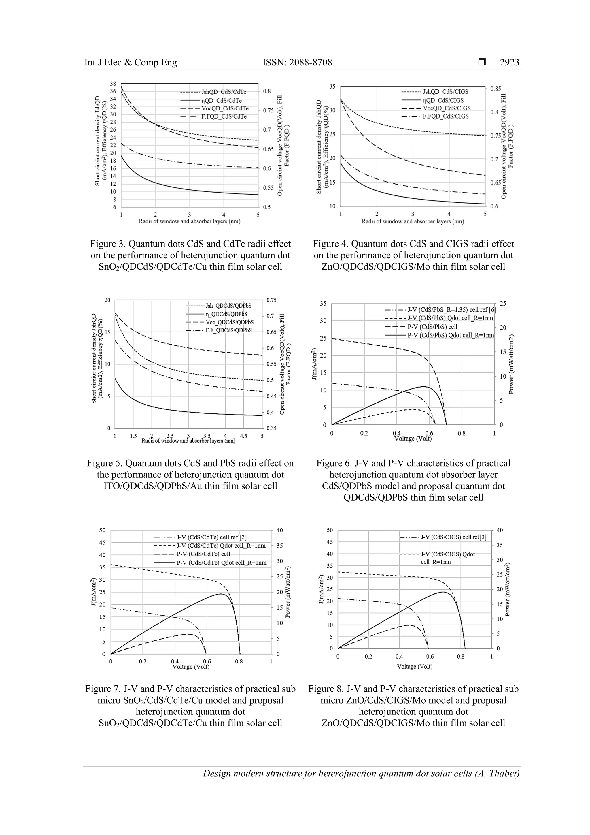
4.2. New heterojunction quantum dot thin film solar cells
Figure 3 illustrates the short circuit current density, open circuit voltage, fill factor and efficiency of
heterojunction quantum dot SnO2/QDCdS/QDCdTe/Cu thin film solar cell with variant quantum dots CdS
and CdTe radii. Whatever, Figure 4 describes the short circuit current density, open circuit voltage, fill factor
and efficiency of heterojunction quantum dot Zno/QDCdS/QDCIGS/Mo thin film solar cell with variant of
quantum dots CdS and CIGS radii. Figure 5 describes the short circuit current density, open circuit voltage,
fill factor and efficiency of heterojunction quantum dot ITO/QDCdS/QDPbS/Au thin film solar cell with
variant radii of quantum dot CdS and PbS. The traditional performance of heterojunction CdS/QDPbS has
been enhanced by replacing the CdS and QDPbS layer with quantum dot QDCdS and QDPbS layers at radii
1nm or 1.35nm. It is noticed that. the best nanoparticles radii for window and absorber layers is 1nm for
enhancing the open circuit voltage, short circuit current density, fill factor and energy conversion efficiency
of the cell.
4.3. Comparison between traditional and heterojunction quantum dots solar cells
Figure 6 illustrated the benefit of using quantum dot size of window layer CdS instead of bulk one
enhanced the absorption of window layer which result more enhancement in J-V and P-V characteristics.
The enhancement in the J-V and P-V characteristics of traditional practical model has been occurred by using
window layer CdS and absorber layer CdTe in quantum dot size with radii 1nm as shown in Figure 7.
On the other hand, Figure 8 shows J-V and P-V characteristics of practical ZnO/CdS/CIGS/Mo model and
proposal heterojunction quantum dot ZnO/QDCdS/QDCIGS/Mo thin film solar cell. Table 4 depicts
the comparison in the performance of practical previous models [2, 3, 6] and the heterojunction quantum dot
proposal models at room temperature. The table show that the performance of selected models has been
enhanced by using window layer and absorber layer in quantum dot size with radii 1nm.
Figure 1. Radii effect on the refractive index and
dielectric constant of quantum dot semiconductors
CdS, CdTe, CIGS and PbS
Figure 2. Radii effect on the absorption coefficient
and energy band gap for quantum dot CdTe, CdS,
PbS and CIGS layers at thickness 700nm](https://image.slidesharecdn.com/v1413dec5dec25mar19781f-201210021708/75/Design-modern-structure-for-heterojunction-quantum-dot-solar-cells-5-2048.jpg)
![ ISSN: 2088-8708
Int J Elec & Comp Eng, Vol. 10, No. 3, June 2020 : 2918 - 2925
2924
Table 4. Comparison between efficiency and electric properties of traditional models and heterojunction
quantum dot proposal models at room temperature
Cells
Open Circuit
Voltage Voc (Volt)
Short Circuit Current
Density Jsh (mA/cm2
)
Fill Factor
F.F
Efficiency
(%)
CdS/ (QDPbS_R=1.35nm) [3] 0.63 12 0.43 3.3
(QDCdS/QDPbS)_R=1nm 0.71 17.75 0.63 7.88
(CdS/CdTe) [4] 0.58 18.6 0.65 4.7
(QDCdS/QDCdTe)_R=1nm 0.81 35.91 0.67 19.36
(CdS/CIGS) [5] 0.59 21 0.685 8.1
(QDCdS/QDCIGS)_R=1nm 0.83 32.43 0.71 19.05
5. THERMAL EFFICIENCY ANALYSIS
Table 5 depicts the thermal effect on efficiency of proposal heterojunction quantum dot
SnO2/QDCdS/QDCdTe/Cu, ZnO/QDCdS/QDCIGS/Mo, ITO/QDCdS/QDPbS/Au thin film solar cells at
various radii of window and absorber layer materials CdS, CdTe. The energy conversion efficiencies of
heterojunction quantum dots proposal thin film solar cells have been higher than the efficiency of practical
models ZnO/CdS/CIGS/Mo, ITO/CdS/QDPbS/Au, SnO2/CdS/CdTe/Cu thin film solar cells under high
thermal conditions.
Table 5. Comparison between proposal selected HJQD thin film solar cells and traditional practical
previous models
Solar Cells
Efficiency %
300K 330 K 350 K 370 K 400 K
ITO/CdS/QDPbS/Au 1.47 1.25 1.11 0.98 0.82
SnO2/CdS/CdTe/Cu 6.15 5.26 4.69 4.13 3.32
ZnO/CdS/CIGS/Mo 8.005 6.61 5.74 4.90 3.71
Efficiency at radii 1nm
ITO/QDCdS/QDPbS/Au 7.88 6.33 5.43 4.63 3.62
SnO2/QDCdS/QDCdTe/Cu 19.36 17.34 16.03 14.75 12.88
ZnO/QDCdS/QDCIGS/Mo 19.05 16.40 14.81 13.31 11.17
Efficiency at radii 1.5nm
ITO/QDCdS/QDPbS/Au 4.57 3.72 3.22 2.78 2.5
SnO2/QDCdS/QDCdTe/Cu 14.38 12.82 11.79 10.78 9.29
ZnO/QDCdS/QDCIGS/Mo 15.08 12.89 11.52 10.22 8.40
Efficiency at radii 2nm
ITO/QDCdS/QDPbS/Au 3.43 2.82 2.45 2.13 1.71
SnO2/QDCdS/QDCdTe/Cu 12.32 10.94 10.03 9.14 7.83
ZnO/QDCdS/QDCIGS/Mo 13.36 11.34 10.08 8.89 7.19
Efficiency at radii 3nm
ITO/QDCdS/QDPbS/Au 2.56 2.12 1.86 1.63 1.32
SnO2/QDCdS/QDCdTe/Cu 10.50 9.29 8.49 7.71 6.6
ZnO/QDCdS/QDCIGS/Mo 11.79 9.93 8.78 7.68 6.11
6. CONCLUSION
The decrease in the grain size of CdTe, CIGS, CdS, PbS semiconductors to quantum dot size
decreased the dielectric constant and refractive index. Whatever, using quantum dot size of CdTe, CIGS,
CdS, PbS semiconductors increased the absorption coefficient of layers and energy band gap. Window and
absorber layers’ materials in quantum size enhanced the energy conversion efficiency, fill factor, short circuit
current density, open circuit voltage of SnO2/CdS/CdTe/Cu, ITO/CdS/QDPbS/Au and ZnO/CdS/CIGS/Mo
thin film solar cells traditional models that are having sub-micro absorber layers’ thicknesses and low
efficiencies. Moreover, the reduction in radii of window and absorber layers materials in quantum dot size to
be 1nm is the best radius for enhancing the performance of heterojunction quantum dot
ITO/QDCdS/QDPbS/Au, ZnO/QDCdS/QDCIGS/Mo and SnO2/QDCdS/QDCdTe/Cu cells due to increasing
the energy band gap of absorber layer and increasing absorption of window and absorber layers which lead to
decreasing the recombination and increasing the open circuit voltage, short circuit current density, output
power density. Decreasing the size of quantum dot window and absorber layers’ materials enhanced
the performance of HJQD proposal selected cells at high temperatures.](https://image.slidesharecdn.com/v1413dec5dec25mar19781f-201210021708/75/Design-modern-structure-for-heterojunction-quantum-dot-solar-cells-7-2048.jpg)
![Int J Elec & Comp Eng ISSN: 2088-8708
Design modern structure for heterojunction quantum dot solar cells (A. Thabet)
2925
ACKNOWLEDGEMENTS
The present work was supported by Nanotechnology Research Center at Aswan University that is
established by aiding the Science and Technology Development Fund (STDF), Egypt, Grant No: Project ID
505, 2009-2011.
REFERENCES
[1] T. Lee, A. Ebong, “A review of Thin Film Solar Cell Technologies and Challenges," Renewable and Sustainable
Energy Reviews, Elsevier, Volume 70, pp. 1286-1297, April 2017.
[2] Z. Bai, J. Yang, S. DePba and D.Wang, "Thin Film CdTe Solar Cells With an Absorber Layer Thickness in Micro-
and Sub-Micrometer scale," Applied Physics Letters, Volume 99, Issue 14, 2011.
[3] O. lundberg, M. Bodegard and L.Stolt, “Influence of the Cu(In,Ga)Se2 Thickness and Grading on Solar Cell
Performance," Progress in Photopholatics: Research and Apblication, Vol. 11, No. 2, pp.77 – 88, 2003.
[4] A. Nozik, "Nanoscience and Nanostructures for Photovoltaics and Solar Fuels. Nano," Nano Letters, Vol. 10,
No. 8, pp. 2735-2741, 2010.
[5] K. Ebrahim, "Quantum Dots Solar Cells," InTech Solar Cells New Approaches and Reviews, Vol. 31, pp.303-331
2015.
[6] K. Bhandari, P. Roland, H. Mahabaduge, N. Haugen, C. Grice, "Thin Film Solar Cells Based on the Heterojunction
of Colloidal PbS Quantum Dots with CdS,” Solar Energy Materials & Solar Cells. Elsevier, Vol. 117,
pp. 476-482, 2013.
[7] M. El-Nahass, G.M. Youssef and Z.Sohaila, “Structural and Optical Characterization of CdTe Quantum Dots Thin
Films," Journal of Alloys and Compounds. Elsevier, Vol. 604, pp.253-259, 2014.
[8] P. Singh, N. Ravindra, “Temperature Dependence of Solar Cell Performance -an analysis," Solar Energy Materials
& Solar Cells. Elsevier, Vol. 101, pp. 36-45, 2012.
[9] Y. Liao, S. Yikuo, W. Tyng, F. Lai, D. Hsieh, “Observation of Unusual Optical Transitions in Thin-Film
Cu(In,Ga)Se2 Solar Cells,” Optics Express, Vol. 20, Issue S6, pp. A836-A842, 2012.
[10] N. Ravindra, S. Auluck, and V. Srivastava, "Temperature Dependence of the Energy Gap in PbS, PbSe, and PbTe,"
Physica Status Solidi, Vol. 52, Issue 2, 1979.
[11] J. Jimenez, W. Tomm, “Spectroscopic Analysis of Optoelectronic Semiconductors,” Springer series in optical
science, pp.27, 2016.
[12] B. K. Ridley, "Quantum Processes in Semiconductors,” 4th Edition. Oxford Science Publications, Ch.16,
Pp.418, 2013.
[13] M.A. Mannan, M.S. Anjan and M.Z. Kabir, “Modeling of Current–Voltage Characteristics of Thin Film Solar
Cells,” Solid-State Electronics. Elsevier, Vol. 63, Issue 1, pp. 49–54, 2011.
[14] R. Das, S. Pandey, "Comparison of Optical Properties of Bulk and Nano Crystalline Thin Films of CdS Using
Different Precursors,” International Journal of Material Science, Vol. 1, Issue 1, pp. 35-40, 2011.
[15] M. Sultan and N. Sultana, "Analysis of Reflectance and Transmittance Characteristics of Optical Thin Film for
Various Film Materials, Thicknesses and Substrates,” J Electr Electron Sys, Vol. 4, Issue 3, 2015.
[16] C. Noguez, "Optical Properties of Isolated and Supported Metal Nanoparticles,” Optical Materials. Elsevier,
Vol. 27, Issue 7, pp. 1204-12011, 2005.
[17] T. Sau, A. Rogach, "Complex Shaped Metal Nanoparticles: Bottom‐Up Syntheses and Applications," Wiley-VCH
Verlag GmbH & Co. KGaA, pp.369, 2012.
[18] Y. Yang, X. Sun, B.J. Chen, T.Chen, C.Sun B.Tay, Z. Sun, "Refractive Indices of Textured Indium Tin Oxide and
Zinc Oxide Thin Films,” Thin Solid Films. Elsevier, Vol. 510, Issue 1-2, pp. 95-101, 2006.
[19] R. Shannona, O. Medenbachb, R. Fischerc, "Refractive Index and Dispersion of Fluorides and Oxides,”
Journal of Physical and Chemical Reference Data, Vol. 31, No. 4, Pp.931-969, 2002.
[20] H.A. Mohamed, "Theoretical Study of the Efficiency of CdS/PbS Thin Film Solar Cells," Solar Energy. Elsevier,
Vol. 108, pp. 360–369, 2014.
[21] R. Prakash, S. Singh, "Designing and modelling of solar photovoltaic cell and array,” IOSR Journal of Electrical
and Electronics Engineering (IOSR-JEEE), Vol. 6,Pp 35-40, 2016.
[22] S. P. Mouri, S. N. Sakib, S. Hoque and M. S. Kaiser, "Theoretical efficiency and cell parameters of AlAs/GaAs/Ge
based new multijunction solar cell," 2016 3rd International Conference on Electrical Engineering and Information
Communication Technology (ICEEICT), Dhaka, pp. 1-6, 2016.
[23] F. Micheal, "Radiative Heat Transfer," 3rd edition. Elsevier, pp. 77, 2013.
[24] B. Yanchuk, "Laser Cleaning: Optical Physics," Applied Physics and Materials Science, pp.136, 2002.
[25] G. Handbush, "Mo Molybdenum: Physical Properties," Part 2. Electrochemistry 8th edition. Springer, pp.62, 2013.
[26] M. Asaduzzaman, M. Hasan and A. Newaz, "An Investigation into The Effects of Band Gap and Doping
Concentration on Cu(In,Ga)Se2 Solar Cell Efficiency," Springer Plus, Vol. 5, No. 1, pp. 1-8, 2016.](https://image.slidesharecdn.com/v1413dec5dec25mar19781f-201210021708/75/Design-modern-structure-for-heterojunction-quantum-dot-solar-cells-8-2048.jpg)