
Recommended
Recommended
More Related Content
What's hot
What's hot (19)
Similar to Original P-Channel Mosfet APM4953 4953 25V 4.9A SOP-8 New Artschip
Similar to Original P-Channel Mosfet APM4953 4953 25V 4.9A SOP-8 New Artschip (20)
More from AUTHELECTRONIC
More from AUTHELECTRONIC (20)
Recently uploaded
Recently uploaded (20)
Original P-Channel Mosfet APM4953 4953 25V 4.9A SOP-8 New Artschip
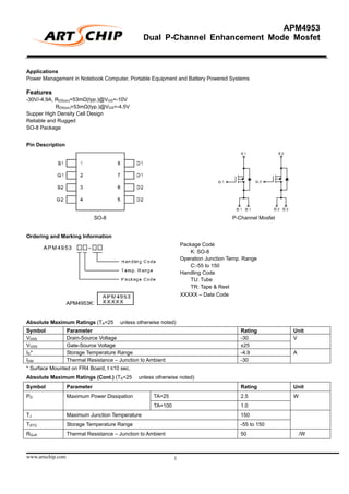
- 1. APM4953 Dual P-Channel Enhancement Mode Mosfet www.artschip.com 1 Applications Power Management in Notebook Computer, Portable Equipment and Battery Powered Systems Features -30V/-4.9A, RDS(on)=53mΩ(typ.)@VGS=-10V RDS(on)=53mΩ(typ.)@VGS=-4.5V Supper High Density Cell Design Reliable and Rugged SO-8 Package Pin Description SO-8 P-Channel Mosfet Ordering and Marking Information Package Code K: SO-8 Operation Junction Temp. Range C:-55 to 150℃ Handling Code TU: Tube TR: Tape & Reel APM4953K: XXXXX – Date Code Absolute Maximum Ratings (TA=25℃ unless otherwise noted) Symbol Parameter Rating Unit VDSS Drain-Source Voltage -30 VGSS Gate-Source Voltage ±25 V ID* Storage Temperature Range -4.9 IDM Thermal Resistance – Junction to Ambient -30 A * Surface Mounted on FR4 Board, t ≤10 sec. Absolute Maximum Ratings (Cont.) (TA=25℃ unless otherwise noted) Symbol Parameter Rating Unit TA=25℃ 2.5PD Maximum Power Dissipation TA=100℃ 1.0 W TJ Maximum Junction Temperature 150 TSTG Storage Temperature Range -55 to 150 ℃ RQJA Thermal Resistance – Junction to Ambient 50 ℃/W
- 2. APM4953 Dual P-Channel Enhancement Mode Mosfet www.artschip.com 2 Electrical Characteristics (TA=25℃ unless otherwise noted) APM4953Symbol Parameter Test Condition Min. Typa. Max Unit Static BVDSS Drain-Source Breakdown Voltage VGS=0V, IDS=-250µA -30 V IDSS Zero Gate Voltage Drain Current VDS=-24V, VGS=0V -1 µA VGS(th) Gate Threshold Voltage VGS=VGS, IDS=-250µA -1 -1.5 -2 V IGSS Gate Leakage Current VGS=±25V, VDS=0V ±100 nA VGS=-10V, IDS=-4.9A 53 60RDS(ON) Drain-Source On-state Resistance b VGS=-4.5V, IDS=-3.6A 80 95 mΩ VSD Diode Forward Voltage b ISD=-1.7A, VGS=0V -0.7 -1.3 V Dynamic a Qg Total Gate Charge 22.3 29 Qgs Gate-Source Charge 4.65 Qgd Gate-Drain Charge VDS=-15V, IGS=-10V ID=-4.6A 2 nC td(on) Turn-on Delay Time 10 18 Tr Turn-on Rise Time 15 20 td(OFF) Turn-off Delay Time 22 38 Tf Turn-off Fall Time VDD=-15V, ID=-2A, VGEN=-10V, RG=6Ω RL=7.5Ω 15 25 ns Ciss Input Capacitance 1260 Coss Output Capacitance 340 Crss Reverse Transfer Capacitance VGS=0V VDS=-25V Frequency=1.0MHz 220 pF Notes a: Pulse test; pulse width ≤300µs, duty cycle ≤2% b: Guaranteed by design, not subject to production testing
- 3. APM4953 Dual P-Channel Enhancement Mode Mosfet www.artschip.com 3 Typical Characteristics Output Characteristics -VDS- Drain-to-Source Voltage (V) Threshold Voltage vs. Junction Temperature On-Resistance vs. Gate-to-Source Voltage -VGS-Gate-to-Source Voltage(V) Transfer Characteristics -VGS – Gate-to-Source Voltage (V) On-Resistance vs. Drain Current On-Resistance Vs. Junction Temperature TJ-Junction Temperature (℃)
- 4. APM4953 Dual P-Channel Enhancement Mode Mosfet www.artschip.com 4 Typical Characteristics (Cont.) Gate Charge QG- Gate Charge (nC) Source-Drain Diode Forward Voltage -VSD – Source-to-Drain Voltage (V) Capacitance -VDS -Drain-to-Source Voltage (V) Single Pulse Power Time (sec) Normalized Thermal Transient Impedance, Junction to Ambient Square Wave Pulse Duration (sec)
- 5. APM4953 Dual P-Channel Enhancement Mode Mosfet www.artschip.com 5 Packaging Information SOP-8 pin (Reference JEDEC Registration MS-012) Millimeters InchesDim Min. Max. Min. Max. A 1.35 1.75 0.053 0.069 A1 0.10 0.25 0.004 0.010 D 4.80 5.00 0.189 0.197 E 3.80 4.00 0.150 0.157 H 5.80 6.20 0.228 0.244 L 0.40 1.27 0.016 0.050 e1 0.33 0.51 0.013 0.020 e2 1.27BSC 0.50BSC Ф1 8˚ 8˚ Physical Specifications Terminal Material Solder-Plated Copper (Solder Material: 90/10 or 63/37 SnPb) Lead Solderability Meets EIA Specification RS186-91, ANSI/J-STD-002 Category 3. Reflow Condition (IR/Convection or VPR Reflow)
- 6. APM4953 Dual P-Channel Enhancement Mode Mosfet www.artschip.com 6 Classification Reflow Profiles Convection or IR/Convection VPR Average ramp-up rate (183℃ to Peak) 3℃/second max. 10℃/second max. Preheat temperature 125 ±25℃ 120 seconds max Temperature maintained above 183℃ 60-150 seconds Time within 5℃ of actual peak temperature 10-20 seconds 60 seconds Peak temperature range 220 +5/-0℃ or 235 +5/-0℃ 215-219℃ or 235 +5/-0℃ Ramp-down rate 6℃/second max. 10℃/second max. Time 25℃ to peak temperature 6 minutes max. Package Reflow Conditions Pkg. thickness ≥2.5mm And all bgas Pkg. thickness <2.5mm and pkg. volume ≥350mm 3 Pkg. thickness < 2.5mm and pkg. Volume <350mm 3 Convection 220 +5/-0 ℃ Convection 235 +5/-0 ℃ VPR 215-219℃ VPR 235 +5/-0℃ IR/Convection 220 +5/-0℃ IR/Convection 235 +5/-0℃ Reliability test program Test item Method Description SOLDERABILITY MIL-STD-883D-2003 245℃, 5 SEC HOLT MIL-STD 883D-1005.7 1000 Hrs Bias @ 125℃ PCT JESD-22-B, A102 168 Hrs, 100% RH,121℃ TST MIL-STD 883D-1011.9 -65℃ ~ 150℃, 200 Cycles Carrier Tape & Reel Dimensions
- 7. APM4953 Dual P-Channel Enhancement Mode Mosfet www.artschip.com 7 Application A B C J T1 T2 W P E 330±1 62+1.5 12.75+0.15 2±0.5 12.4±0.2 2±0.2 12±0.3 8±0.1 1.75±0.1 F D D1 Po P1 Ao Bo Ko t SOP-8 5.5±1 1.55+0.1 1.55+0.25 4.0±0.1 2.0±0.1 6.4±0.1 5.2±0.1 2.1±0.1 0.3±0.013 Cover Tape Dimensions Application Carrier Width Cover Tape Width Devices Per Reel SOP-8 12 9.3 2500