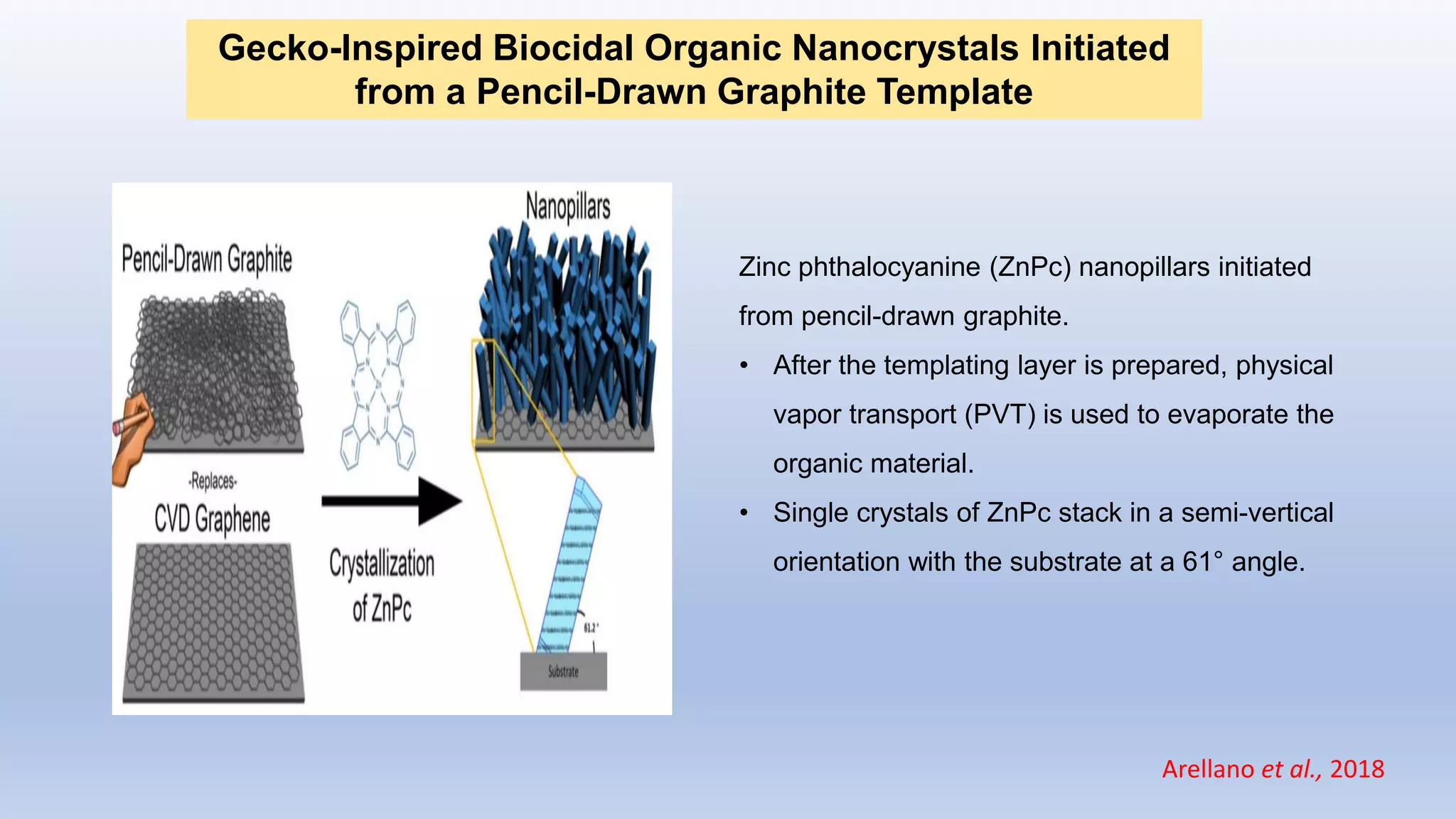
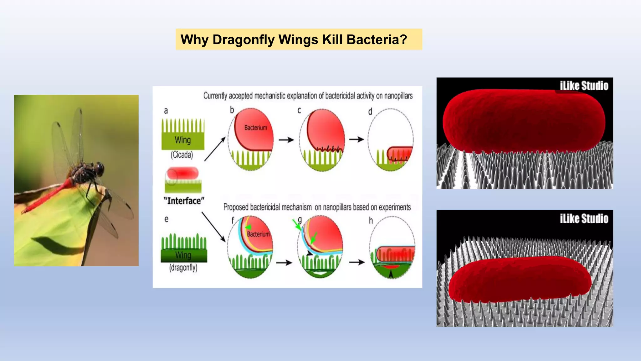
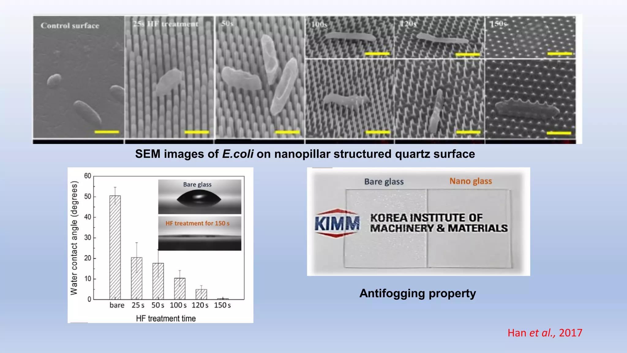
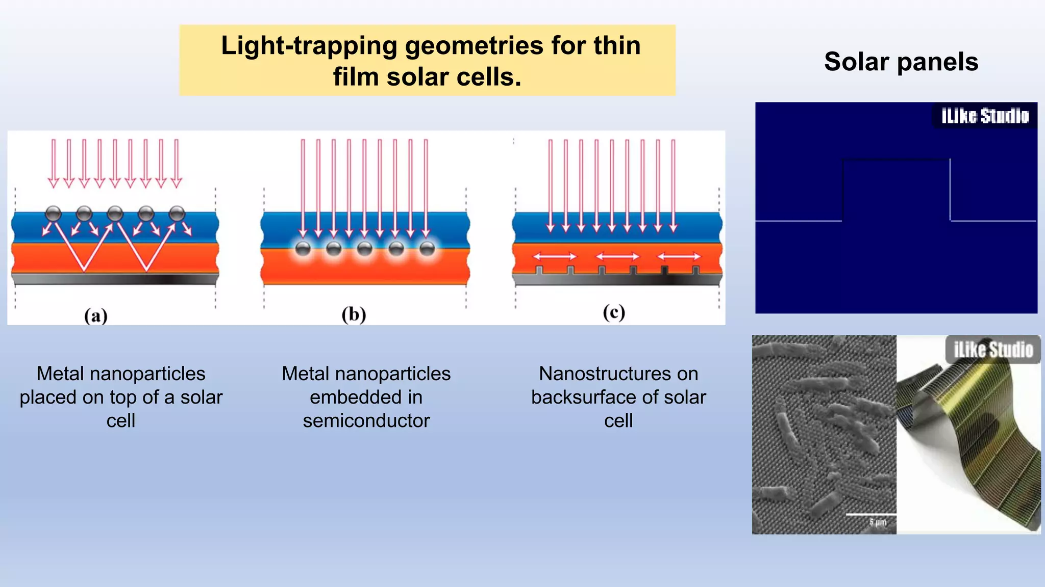
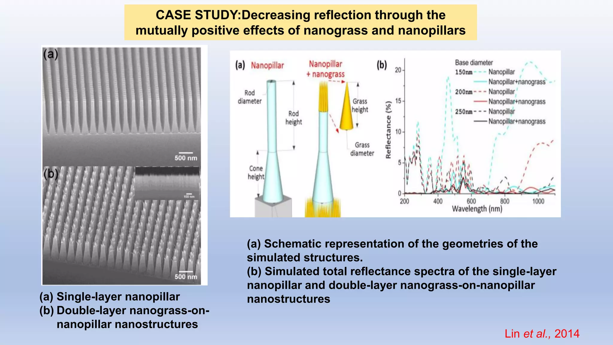
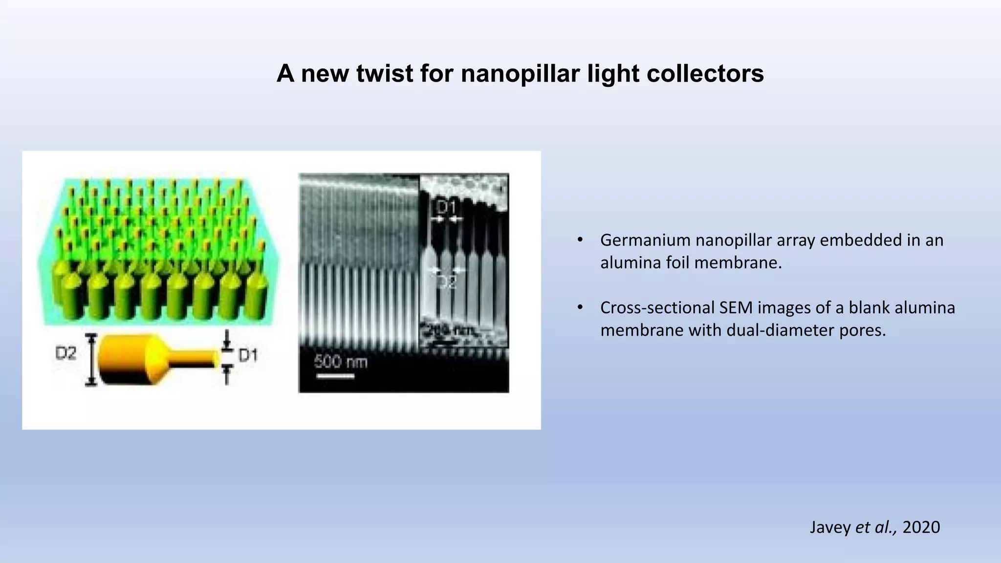
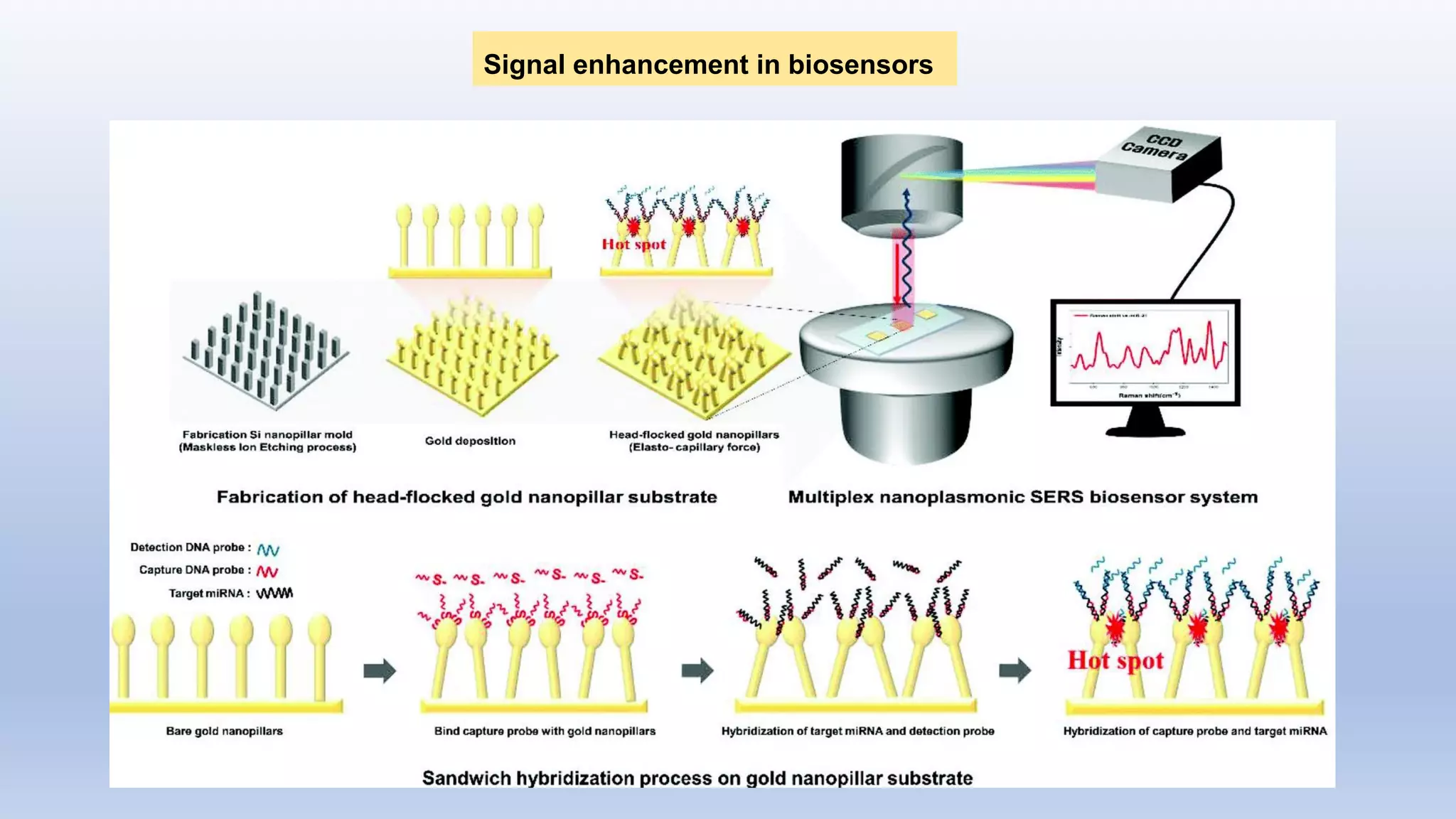
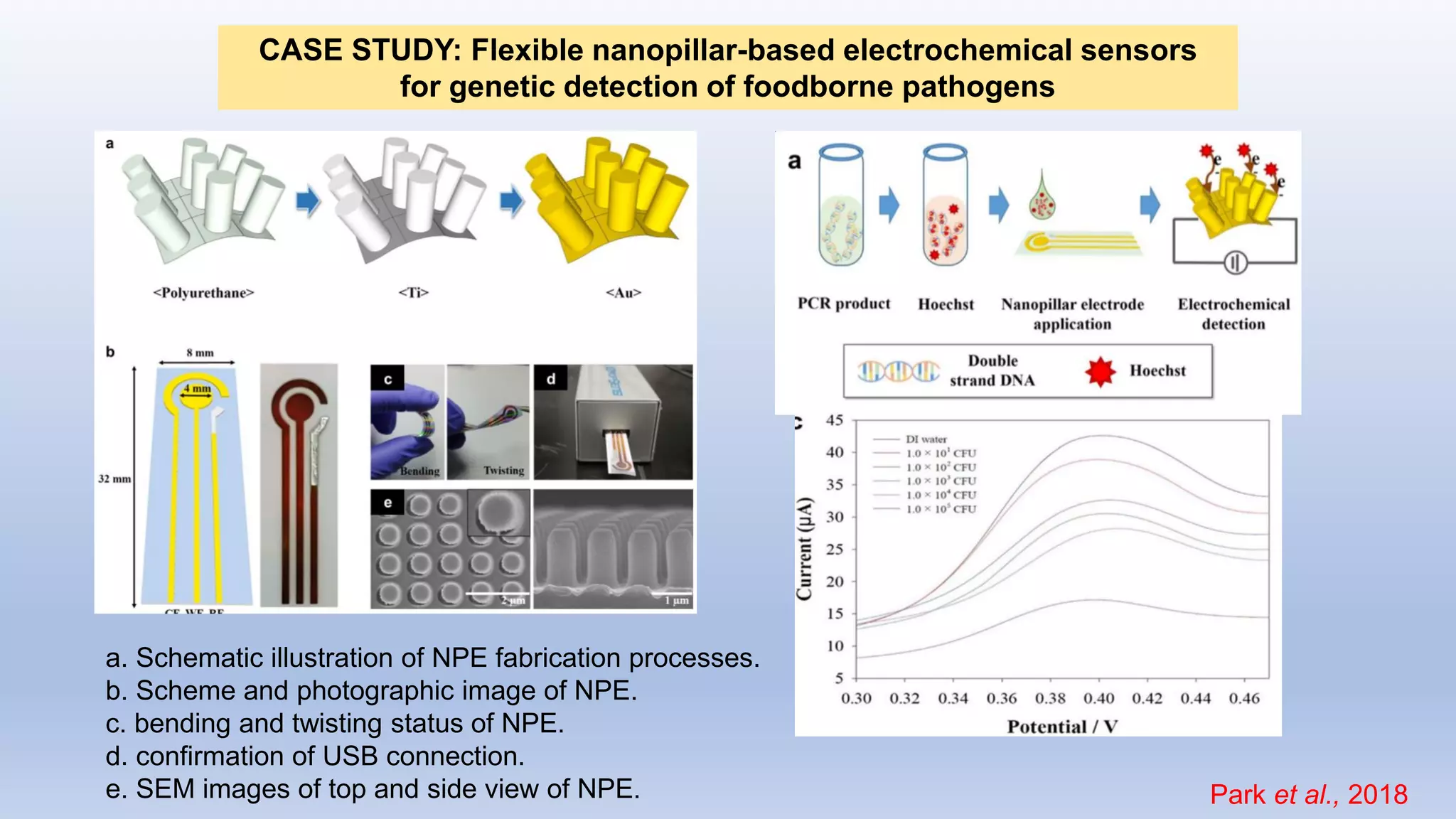
Download as PDF, PPTX


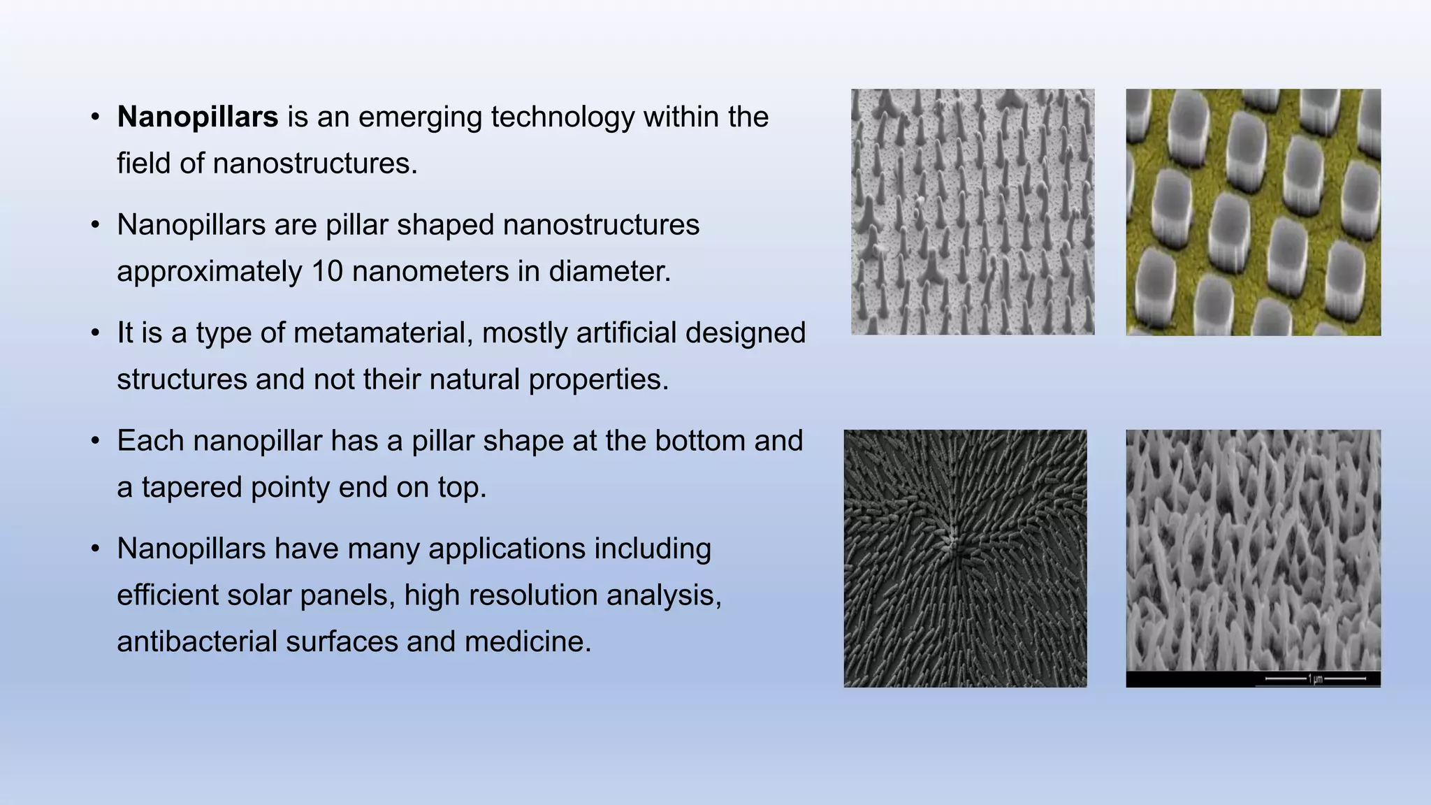
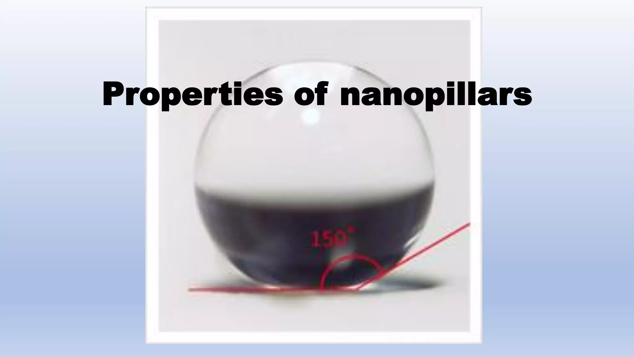


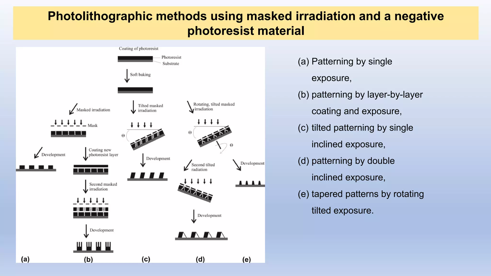
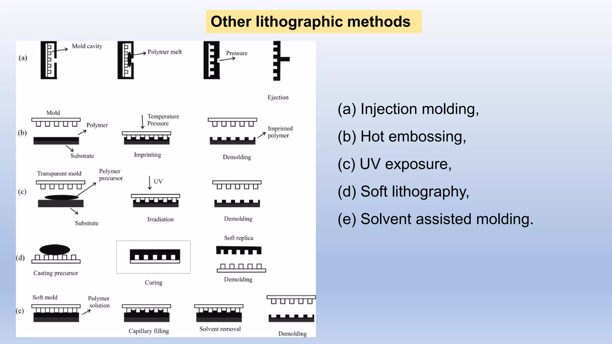


This document discusses nanopillars, which are pillar-shaped nanostructures approximately 10 nanometers in diameter. It describes various properties and fabrication methods of nanopillars, including their increased surface area, mechanical stability, optical characteristics, and biocompatibility. Case studies are presented on the synthesis of nanopillars using top-down lithography approaches as well as bottom-up growth techniques. Applications of nanopillars in areas such as antibacterial coatings, optics, energy, and biosensing are explored through additional case studies. The document concludes by stating that nanopillars provide many advantages for applications in biomedical, energy, and agricultural fields due to their vertically aligned nature and ability to be easily fabricated.