The document is a data sheet for the AD590 integrated circuit temperature transducer. It provides specifications for the device such as a linear current output of 1 μA/K, a temperature range of -55°C to +150°C, and a calibration accuracy of ±0.5°C. It also describes features of the device such as its 2-terminal design, wide power supply range, and sensor isolation from the case. Application examples include temperature measurement, compensation, and remote sensing.
This 3 sentence summary provides the key details about the Analog Multiplier Data Sheet:
The data sheet describes the AD633 analog multiplier chip, which features 4-quadrant multiplication, low cost packaging, and laser-trimmed accuracy within 2% of full scale. The AD633 has high impedance differential inputs and a unity-gain summing input, making it suitable for applications involving multiplication, division, modulation, filtering and more. The document provides specifications, application information, and evaluation board details for the AD633 analog multiplier.
Original High Voltage Isolation IC ACS710T KLA-12CB 710T SOP-16 NewAUTHELECTRONIC
The Allegro ACS710 current sensor provides economical and precise current sensing for industrial, commercial, and communications systems. It uses a precision linear Hall sensor integrated circuit with a copper conduction path near the surface to linearly track the magnetic field generated by the applied current. The sensor offers high immunity to electrical noise and low offset drift, and provides an analog output voltage and integrated overcurrent detection. It is available in a small surface-mount package.
The AD620 is a low cost, low power instrumentation amplifier that requires only one external resistor to set gains between 1 and 10,000. It has high accuracy, low offset voltage and drift, low noise, and works from supply voltages of ±2.3V to ±18V. The AD620 is suitable for use in precision measurement applications such as medical equipment, weighing scales, and data acquisition systems.
This document provides information on the MS 2x series of exposed linear encoders from Electromate, including:
- The encoders use a scanning principle that produces highly accurate sinusoidal signals with minimal sensitivity to contamination on the scale.
- Models include options for voltage or square wave outputs, integrated interpolation, reference marks, and switch signals.
- They are designed for applications requiring high speeds up to 10 m/s, large mounting tolerances, and resolutions down to 100 nm.
The document provides information on the S 200 S miniature circuit breaker from ABB. It has a screwless terminal that allows for quick and easy wiring without tools. Various cable types can be directly connected to the terminal. The breaker extends ABB's System pro M compact product range and offers faster installation than standard screw-type breakers. It provides overcurrent and short circuit protection for circuits up to 20A.
The document describes a 20mA LED driver demo board that operates from 10-400V DC or 10-265V AC input and can power a single 20mA LED or string of LEDs up to 9V. The circuit uses an HV9821 control IC to operate in three modes - clamped buck converter, buck converter, or resistive ballast - depending on the line and load conditions. The board is designed to meet EMI standards and provides LED current regulation within 3% over the input voltage range while consuming less than 1W of power.
This document provides a summary of the L293 and L293D integrated circuits. The L293 and L293D are quadruple half-H drivers designed to provide bidirectional drive currents of up to 1A and 600mA respectively. They can be used to drive inductive loads such as relays, solenoids, DC motors, and stepping motors. Key features include a wide supply voltage range of 4.5V to 36V, separate logic and output supplies, internal ESD protection, and thermal shutdown protection. The document provides pinout diagrams, electrical specifications, and an application circuit for driving a two-phase motor.
This document provides instructions for the CT-2000ES inverter unit. It includes:
1) An overview of inspection, installation, storage, dimensions and application notes for the inverter unit.
2) Details on wiring the main and control circuits, connecting the power supply and motor, and using a power source reactor and brake resistor.
3) Instructions for operation testing and adjusting functions via the keypad, including display specifications and function codes.
4) Descriptions of alarm displays, troubleshooting, maintenance, specifications and communication protocols.
This document describes a pulse counter circuit using an AT89C4051 microcontroller. It includes a circuit schematic and descriptions of the major components used, including the AT89C4051 microcontroller, MAX232 RS-232 driver, 7805 voltage regulator, LCD display, 11.0592MHz crystal, and other passive components. The circuit uses the microcontroller to count input pulses and display the count on the LCD. Hardware and functionality of the components are explained in detail.
1. The document is a service manual that provides specifications and adjustment procedures for a colour television.
2. It includes block diagrams of the chassis and ICs, safety notices, a parts list, and an on-screen service menu table with initial values and adjustment ranges for various service menu items.
3. The service menu can be accessed by pressing buttons on the remote while holding the TV menu button, and allows remote adjustment of items like colour balance, geometry, etc. The adjusted values are stored in memory.
16 Terminal block
28 Terminal adapter (TA)
8 Lifting hole
17 Terminal adapter (TA)
29 Neutral CT (NCT)
9 Drawout handle
18 External ZCT (ZCT)
30 External ZCT (ZCT)
10 Drawout position indicator
19 ETR external unit
31 Panel cut (PC)
11 Charging handle
20 Drawout handle (DH)
This document describes Mitsubishi's WS series of low voltage air circuit breakers ranging from 630A to 6300A. It provides an overview of the product line up and highlights key features such as best solution,
Original Power Supply IC LNK626PG LNK626P LNK626 DIP-7 New Power IntegrationAUTHELECTRONIC
Original Power Supply IC LNK626PG LNK626P LNK626 DIP-7 New Power Integration
https://authelectronic.com/original-power-ic-lnk626pg-lnk626p-lnk626-dip-7-new-power-integration
This document provides instructions for the control circuit of KEB COMBIVERT F5 frequency inverters. It describes the assignment of terminals on the control terminal strip X2A and how to connect the control circuit. It also outlines the operation of the optional operator interface used for parameter input and drive control.
The LM3914 is an integrated circuit that senses analog voltage levels and drives 10 LEDs to provide a linear analog display. It contains an adjustable voltage reference and accurate 10-step voltage divider to compare input voltages. The outputs are individually current regulated and can drive LEDs, LCDs, or vacuum fluorescent displays in either a moving dot or bar graph display mode. The simple circuit requires few external components and can operate over a wide supply voltage range from less than 3V.
The MAX232 device is a dual driver/receiver that converts between TTL/CMOS and RS-232 signal levels. It contains a charge pump that generates the voltages required by RS-232 from a single 5V supply. Each receiver converts ±30V RS-232 signals to 5V TTL/CMOS levels, and each driver converts TTL/CMOS signals to RS-232 levels. It is commonly used to interface between RS-232 ports and devices that use lower voltage digital levels like microcontrollers.
This 3 sentence summary provides the key details about the AD584 precision voltage reference data sheet:
The AD584 is a precision voltage reference chip that provides 4 programmable output voltages of 10V, 7.5V, 5V, and 2.5V without external components. It uses laser trimming to achieve very low errors and temperature coefficients over its operating temperature range. The data sheet provides specifications, application information, and diagrams on how to use the various features of the AD584 voltage reference.
This document provides an installation and user manual for the CHOPPER SEM2 electronic speed controller.
It begins with an introduction to the ZAPI-MOS family of speed controllers and their key features including advanced technology, flexibility, safety, and openness to future innovations.
The document then provides details on the technical specifications, control units, safety features, directions, operations, diagnostics, thermal considerations, and instructions for the SEM2 speed controller. It includes sections on installation, programming adjustments, traction applications, diagnostics, spare parts, and maintenance.
Please read the manual carefully before using the product. The pictures, marks and
symbol in the manual belong to Acrel. The manual or part of it shall not be publicly
reprinted by people outside the company without written authorization.
This document provides data sheets for several quad operational amplifier integrated circuits, including the CA124, CA224, CA324, LM324, and LM2902. It summarizes their key specifications such as operating temperature range, voltage gain, bandwidth, input/output voltage ranges, power requirements, and packaging options. The amplifiers each contain four independent high-gain op-amps on a single chip and are designed for use in commercial, industrial and military applications requiring operation from single or dual power supplies.
With the WiDom flush-mounted Double Switch Relay, you can integrate existing electrical installations (e.g. lighting, airing systems…) into a Z-Wave network.
This document provides information on Fuji Electric's magnetic contactors and starters, including the SC and SW series. It describes the key features and advantages of these products, such as their modular design that allows for easy addition of functions, long electrical life, wide voltage ratings, and bifurcated auxiliary contacts. The SC-N series is highlighted for using an electronically-controlled SUPER MAGNET coil that provides positive pick-up and drop-out without chattering across a wide voltage range on both AC and DC power supplies. Safety features like terminal covers and insulation barriers are also summarized.
8 inch TFT-LCD Datesheet, AUO, 800*1280, MIPI InterfacePanox Display
Display Brand AUO
Interface MIPI
Screen Size 8 inch
Orientation Portrait
Display Color Full Color
Manufacturer Panox Display
Resolution 800x1280
Driver IC ER88577
HDMI Controller Board Available
For more
https://www.panoxdisplay.com/tft-lcd/8-inch-tft-lcd-800x1280-mipi.html
The document provides instructions for installing and operating a WiDom Smart Double Switch. It allows independent control of two loads and can be operated by both local and remote switches. It includes in Z-Wave networks and supports association groups to control other devices. Configuration parameters allow customizing switch behavior for load control via clicks on external switches and timers.
This document contains a wiring diagram with various electrical components labeled. It includes labels for terminals, voltage levels, motor connections, overload relays, contactors, transformers, resistors, and more. The diagram shows connections between a power supply, motor, and control components like overloads and contactors.
K30 controller is intended for permanent installation, for
indoor use only, in an electrical panel which encloses the
rear housing, exposed terminals and wiring on the back.
This document provides installation and configuration instructions for the TECNOLOGIC K series controller. It outlines the mounting requirements including dimensions, environmental conditions and panel thickness. It describes the input/output connections and wiring diagrams. The configuration procedure involves entering password-protected modes to modify parameter groups that control functions like control strategy, alarms and outputs. The factory default parameters can be restored for reconfiguration.
This document provides an overview and specifications for the Q46C2 2-electrode conductivity monitor/analyzer. It includes:
1. General features such as power options, outputs, display, and sensor compatibility.
2. Specifications for measurement ranges, outputs, relays, enclosure, and performance.
3. Instructions for mounting the analyzer including wall/pipe mounting, panel mounting, and sensor mechanicals.
4. Details on electrical installation including power, relay, output, and sensor connections.
5. Description of the user interface and software including menus, calibration, PID control, and diagnostics.
6. Information on system configuration, maintenance, calibration procedures, spare parts,
`The AN5277 is an integrated circuit (IC) amplifier widely used in audio applications, offering excellent audio quality and performance. Designed specifically for audio amplification, the AN5277 provides a compact and efficient solution for various audio systems, including portable devices, multimedia speakers, and automotive audio systems.
The document describes the HT12D and HT12F decoders. The decoders receive serial addresses and data from encoders and decode the information. The HT12D provides 8 address bits and 4 data bits as outputs, while the HT12F decodes 12 address bits and provides a momentary valid transmission indicator. The decoders operate between 2.4-12V and require a resistor connected oscillator to function properly paired with Holtek encoders.
The document describes two CMOS LSIs, the HT12A and HT12E, which are encoders for remote control systems. They can encode information consisting of N address bits and 12-N data bits. The HT12A provides a 38kHz carrier for infrared transmission and allows selection of a data trigger, while the HT12E allows selection of a TE trigger. Upon receiving a trigger signal, the encoded addresses and data are transmitted in a series of words via an RF or infrared medium.
The document is a reference manual for the MFR4310 FlexRay controller. It provides an overview of the device, including its features, block diagram, signal descriptions, modes of operation and external interfaces. It also describes in detail the various modules within the FlexRay controller, including the FlexRay communication module, port integration module, voltage regulator and oscillator. The reference manual provides memory maps and detailed descriptions of the registers for configuration and control of the FlexRay controller functionality.
This document provides a summary of changes made in Revision 2 of the MC13202 datasheet from Freescale Semiconductor. The revision includes an addendum describing changes made to Revision 1.5, as well as the original Revision 1.5 datasheet. The addendum describes two changes: 1) a change to the case outline drawing for a new QFN-32 package, and 2) removal of references to case 1311-03. The full Revision 1.5 datasheet is then provided, describing the MC13202 low power transceiver chip.
The TDA5051A is a modem IC designed for ASK data transmission over home power lines at 600 or 1200 baud. It features fully digital carrier generation and modulation/demodulation, with an integrated output power stage. The IC requires few external components and operates from a single 5V supply. It is intended for applications such as home automation, energy control, and transmitting data over power lines using amplitude shift keying modulation at carrier frequencies up to 132.5 kHz.
This document provides an overview and evaluation of the A5191HRTNGEVB evaluation board, which demonstrates the external components needed for operating the A5191HRT IC for HART communications. The board allows testing the IC's small PCB footprint and easy design of HART implementations. Key sections described include the power supply, reference voltages, clock generation, and schematic. Electrical characteristics and a bill of materials are also provided.
3 Simple Steps To Buy Verified Payoneer Account In 2024SEOSMMEARTH
Buy Verified Payoneer Account: Quick and Secure Way to Receive Payments
Buy Verified Payoneer Account With 100% secure documents, [ USA, UK, CA ]. Are you looking for a reliable and safe way to receive payments online? Then you need buy verified Payoneer account ! Payoneer is a global payment platform that allows businesses and individuals to send and receive money in over 200 countries.
If You Want To More Information just Contact Now:
Skype: SEOSMMEARTH
Telegram: @seosmmearth
Gmail: seosmmearth@gmail.com
Company Valuation webinar series - Tuesday, 4 June 2024FelixPerez547899
This session provided an update as to the latest valuation data in the UK and then delved into a discussion on the upcoming election and the impacts on valuation. We finished, as always with a Q&A
Structural Design Process: Step-by-Step Guide for BuildingsChandresh Chudasama
The structural design process is explained: Follow our step-by-step guide to understand building design intricacies and ensure structural integrity. Learn how to build wonderful buildings with the help of our detailed information. Learn how to create structures with durability and reliability and also gain insights on ways of managing structures.
SATTA MATKA SATTA FAST RESULT KALYAN TOP MATKA RESULT KALYAN SATTA MATKA FAST RESULT MILAN RATAN RAJDHANI MAIN BAZAR MATKA FAST TIPS RESULT MATKA CHART JODI CHART PANEL CHART FREE FIX GAME SATTAMATKA ! MATKA MOBI SATTA 143 spboss.in TOP NO1 RESULT FULL RATE MATKA ONLINE GAME PLAY BY APP SPBOSS
Storytelling is an incredibly valuable tool to share data and information. To get the most impact from stories there are a number of key ingredients. These are based on science and human nature. Using these elements in a story you can deliver information impactfully, ensure action and drive change.
How are Lilac French Bulldogs Beauty Charming the World and Capturing Hearts....Lacey Max
“After being the most listed dog breed in the United States for 31
years in a row, the Labrador Retriever has dropped to second place
in the American Kennel Club's annual survey of the country's most
popular canines. The French Bulldog is the new top dog in the
United States as of 2022. The stylish puppy has ascended the
rankings in rapid time despite having health concerns and limited
color choices.”
Building Your Employer Brand with Social MediaLuanWise
Presented at The Global HR Summit, 6th June 2024
In this keynote, Luan Wise will provide invaluable insights to elevate your employer brand on social media platforms including LinkedIn, Facebook, Instagram, X (formerly Twitter) and TikTok. You'll learn how compelling content can authentically showcase your company culture, values, and employee experiences to support your talent acquisition and retention objectives. Additionally, you'll understand the power of employee advocacy to amplify reach and engagement – helping to position your organization as an employer of choice in today's competitive talent landscape.
The Genesis of BriansClub.cm Famous Dark WEb PlatformSabaaSudozai
BriansClub.cm, a famous platform on the dark web, has become one of the most infamous carding marketplaces, specializing in the sale of stolen credit card data.
❼❷⓿❺❻❷❽❷❼❽ Dpboss Matka Result Satta Matka Guessing Satta Fix jodi Kalyan Final ank Satta Matka Dpbos Final ank Satta Matta Matka 143 Kalyan Matka Guessing Final Matka Final ank Today Matka 420 Satta Batta Satta 143 Kalyan Chart Main Bazar Chart vip Matka Guessing Dpboss 143 Guessing Kalyan night
Understanding User Needs and Satisfying ThemAggregage
https://www.productmanagementtoday.com/frs/26903918/understanding-user-needs-and-satisfying-them
We know we want to create products which our customers find to be valuable. Whether we label it as customer-centric or product-led depends on how long we've been doing product management. There are three challenges we face when doing this. The obvious challenge is figuring out what our users need; the non-obvious challenges are in creating a shared understanding of those needs and in sensing if what we're doing is meeting those needs.
In this webinar, we won't focus on the research methods for discovering user-needs. We will focus on synthesis of the needs we discover, communication and alignment tools, and how we operationalize addressing those needs.
Industry expert Scott Sehlhorst will:
• Introduce a taxonomy for user goals with real world examples
• Present the Onion Diagram, a tool for contextualizing task-level goals
• Illustrate how customer journey maps capture activity-level and task-level goals
• Demonstrate the best approach to selection and prioritization of user-goals to address
• Highlight the crucial benchmarks, observable changes, in ensuring fulfillment of customer needs
B2B payments are rapidly changing. Find out the 5 key questions you need to be asking yourself to be sure you are mastering B2B payments today. Learn more at www.BlueSnap.com.
[To download this presentation, visit:
https://www.oeconsulting.com.sg/training-presentations]
This PowerPoint compilation offers a comprehensive overview of 20 leading innovation management frameworks and methodologies, selected for their broad applicability across various industries and organizational contexts. These frameworks are valuable resources for a wide range of users, including business professionals, educators, and consultants.
Each framework is presented with visually engaging diagrams and templates, ensuring the content is both informative and appealing. While this compilation is thorough, please note that the slides are intended as supplementary resources and may not be sufficient for standalone instructional purposes.
This compilation is ideal for anyone looking to enhance their understanding of innovation management and drive meaningful change within their organization. Whether you aim to improve product development processes, enhance customer experiences, or drive digital transformation, these frameworks offer valuable insights and tools to help you achieve your goals.
INCLUDED FRAMEWORKS/MODELS:
1. Stanford’s Design Thinking
2. IDEO’s Human-Centered Design
3. Strategyzer’s Business Model Innovation
4. Lean Startup Methodology
5. Agile Innovation Framework
6. Doblin’s Ten Types of Innovation
7. McKinsey’s Three Horizons of Growth
8. Customer Journey Map
9. Christensen’s Disruptive Innovation Theory
10. Blue Ocean Strategy
11. Strategyn’s Jobs-To-Be-Done (JTBD) Framework with Job Map
12. Design Sprint Framework
13. The Double Diamond
14. Lean Six Sigma DMAIC
15. TRIZ Problem-Solving Framework
16. Edward de Bono’s Six Thinking Hats
17. Stage-Gate Model
18. Toyota’s Six Steps of Kaizen
19. Microsoft’s Digital Transformation Framework
20. Design for Six Sigma (DFSS)
To download this presentation, visit:
https://www.oeconsulting.com.sg/training-presentations
At Techbox Square, in Singapore, we're not just creative web designers and developers, we're the driving force behind your brand identity. Contact us today.
Anny Serafina Love - Letter of Recommendation by Kellen Harkins, MS.AnnySerafinaLove
This letter, written by Kellen Harkins, Course Director at Full Sail University, commends Anny Love's exemplary performance in the Video Sharing Platforms class. It highlights her dedication, willingness to challenge herself, and exceptional skills in production, editing, and marketing across various video platforms like YouTube, TikTok, and Instagram.
The 10 Most Influential Leaders Guiding Corporate Evolution, 2024.pdfthesiliconleaders
In the recent edition, The 10 Most Influential Leaders Guiding Corporate Evolution, 2024, The Silicon Leaders magazine gladly features Dejan Štancer, President of the Global Chamber of Business Leaders (GCBL), along with other leaders.
2. AD590 Data Sheet
Rev. G | Page 2 of 16
TABLE OF CONTENTS
Features.....................................................................................1
General Description..................................................................1
Pin Configurations....................................................................1
Product Highlights....................................................................1
Revision History........................................................................2
Specifications.............................................................................3
AD590J and AD590KSpecifications......................................3
AD590L and AD590M Specifications....................................4
Absolute Maximum Ratings......................................................5
ESD Caution..........................................................................5
Product Description..................................................................6
Explanation of Temperature Sensor Specifications................7
Calibration Error...................................................................7
Error vs. Temperature: Calibration Error Trimmed Out........7
Error vs. Temperature: No User Trims...................................7
Nonlinearity ..........................................................................8
Voltage and Thermal Environment Effects............................8
General Applications...............................................................10
Outline Dimensions................................................................13
Ordering Guide ...................................................................15
REVISION HISTORY
1/13—Rev. F to Rev. G
Changes to Endnote 2, Table 1...................................................3
Changes to Ordering Guide.....................................................15
11/12—Rev. E to Rev. F
Added 4-Lead LFCSP_WD ......................................... Universal
Changes to Features Section, General Description Section, and
Product Highlights Section........................................................1
Added Figure 2; Renumbered Sequentially................................1
Added Note 2, Table 1; Renumbered Sequentially.....................3
Changes to (Unbolded) For 8-Lead SOIC Package, AD590J and
AD590K Parameter, Table 1.......................................................3
Changes to Note 1, Table 3.........................................................5
Changes to Product Description Section...................................6
Change to Figure 6.....................................................................6
Changes to Explanation of Temperature Sensor Specifications
Section.......................................................................................7
Moved Nonlinearity Section......................................................8
Change to Figure 13...................................................................8
Changes to General Applications Section................................10
Changes to Figure 17 and Figure 19.........................................10
Deleted Figure 22; Renumbered Sequentially..........................11
Changes to Figure 21 and Figure 22........................................11
Deleted Figure 24....................................................................12
Changes to Figure 24...............................................................12
Updated Outline Dimensions Section.....................................14
Changes to Ordering Guide.....................................................14
9/09—Rev. D to Rev. E
Changes to Product Description Section...................................6
Updated Outline Dimensions..................................................13
Changes to Ordering Guide.....................................................14
1/06—Rev. C to Rev. D
Updated Format...........................................................Universal
Changes to Figure 4 Equation....................................................4
9/03—Rev. B to Rev. C
Added SOIC-8 Package................................................Universal
Change to Figure 1 ....................................................................1
Updated Outline Dimensions..................................................13
Added Ordering Guide............................................................14
3. Data Sheet AD590
Rev. G | Page 3 of 16
SPECIFICATIONS
AD590J AND AD590K SPECIFICATIONS
25°C and VS = 5 V, unless otherwise noted.1
Table 1.
AD590J2
AD590K
Parameter Min Typ Max Min Typ Max Unit
POWER SUPPLY
OperatingVoltage Range 4 30 4 30 V
OUTPUT
Nominal Current Output @ 25°C (298.2 K) 298.2 298.2 µA
Nominal Temperature Coefficient 1 1 µA/K
CalibrationError @ 25°C ±5.0 ±2.5 °C
Absolute Error (Over Rated Performance Temperature Range)
Without External CalibrationAdjustment ±10 ±5.5 °C
With25°C CalibrationError Set to Zero ±3.0 ±2.0 °C
Nonlinearity
For TO-52 and FLATPACK Packages ±1.5 ±0.8 °C
For 8-Lead SOIC Package ±1.5 ±1.0 °C
For 4-Lead LFCSP Package ±1.5 °C
Repeatability3
±0.1 ±0.1 °C
Long-Term Drift4
±0.1 ±0.1 °C
CurrentNoise 40 40 pA/√Hz
PowerSupply Rejection
4 V ≤ VS ≤ 5 V 0.5 0.5 µA/V
5 V ≤ VS ≤ 15 V 0.2 0.2 µV/V
15 V ≤ VS ≤ 30 V 0.1 0.1 µA/V
Case Isolation to Either Lead 1010
1010
Ω
Effective Shunt Capacitance 100 100 pF
Electrical Turn-On Time 20 20 µs
Reverse Bias Leakage Current(Reverse Voltage = 10 V)5
10 10 pA
1 Specificationsshowninboldface are testedonallproductionunitsat finalelectricaltest. Resultsfromthose testsare usedtocalculate outgoingqualitylevels. All
minimum andmaximum specificationsare guaranteed,althoughonlythose showninboldfaceare testedonallproductionunits.
2
The LFCSP package hasareducedoperatingtemperature range of −40°Cto+125°C.
3 Maximum deviationbetween+25°Creadingsaftertemperature cyclingbetween−55°Cand+150°C; guaranteed, nottested.
4 Conditions: constant5 V, constant125°C;guaranteed,nottested.
5 Leakage currentdoublesevery10°C.
4. AD590 Data Sheet
Rev. G | Page 4 of 16
AD590L AND AD590M SPECIFICATIONS
25°C and VS = 5 V, unless otherwise noted.1
Table 2.
AD590L AD590M
Parameter Min Typ Max Min Typ Max Unit
POWER SUPPLY
Operating Voltage Range 4 30 4 30 V
OUTPUT
Nominal Current Output @ 25°C (298.2 K) 298.2 298.2 μA
Nominal Temperature Coefficient 1 1 μA/K
Calibration Error @ 25°C ±1.0 ±0.5 °C
Absolute Error (Over Rated Performance Temperature Range) °C
Without External Calibration Adjustment ±3.0 ±1.7 °C
With ± 25°C Calibration Error Set to Zero ±1.6 ±1.0 °C
Nonlinearity ±0.4 ±0.3 °C
Repeatability2
±0.1 ±0.1 °C
Long-Term Drift3
±0.1 ±0.1 °C
Current Noise 40 40 pA/√Hz
Power Supply Rejection
4 V ≤ VS ≤ 5 V 0.5 0.5 μA/V
5 V ≤ VS ≤ 15 V 0.2 0.2 μA/V
15 V ≤ VS ≤ 30 V 0.1 0.1 μA/V
Case Isolation to Either Lead 1010
1010
Ω
Effective Shunt Capacitance 100 100 pF
Electrical Turn-On Time 20 20 μs
Reverse Bias Leakage Current (Reverse Voltage = 10 V)4
10 10 pA
1
Specifications shown in boldface are tested on all production units at final electrical test. Results from those tests are used to calculate outgoing quality levels. All
minimum and maximum specifications are guaranteed, although only those shown in boldface are tested on all production units.
2
Maximum deviation between +25°C readings after temperature cycling between −55°C and +150°C; guaranteed, not tested.
3
Conditions: constant 5 V, constant 125°C; guaranteed, not tested.
4
Leakage current doubles every 10°C.
15
.
273
32
9
5
C
K
F
C
7
.
459
32
5
9
F
R
C
F
Figure 5. Temperature Scale Conversion Equations
00533-002
+223°
–50°
+273°
0°
+298°
+25°
+323°
+50°
+373°
+100°
+423°
+150°
–100° 0° +100° +200° +300°
+32° +70° +212°
°K
°C
°F
5. Data Sheet AD590
Rev. G | Page 5 of 16
ABSOLUTE MAXIMUM RATINGS
Table 3.
Parameter Rating
Forward Voltage ( E+ or E−) 44 V
Reverse Voltage (E+ to E−) −20 V
Breakdown Voltage (Case E+ or E−) ±200 V
Rated Performance Temperature Range1
−55°C to +150°C
Storage Temperature Range1
−65°C to +155°C
Lead Temperature (Soldering, 10 sec) 300°C
1
The AD590 was used at −100°C and +200°C for short periods of
measurement with no physical damage to the device. However, the absolute
errors specified apply to only the rated performance temperature range.
Applicable to 2-lead FLATPACK and 3-pin TO-52 packages only.
Stresses above those listed under Absolute Maximum Ratings
may cause permanent damage to the device. This is a stress
rating only and functional operation of the device at these or
any other conditions above those indicated in the operational
section of this specification is not implied. Exposure to absolute
maximum rating conditions for extended periods may affect
device reliability.
ESD CAUTION
6. AD590 Data Sheet
Rev. G | Page 6 of 16
PRODUCT DESCRIPTION
The AD590 is a 2-terminal temperature-to-voltage transducer. It
is available in a variety of accuracy grades and packages. When
using the AD590 in die form, the chip substrate must be kept
electrically isolated (floating) for correct circuit operation.
Figure 6. Metallization Diagram
The AD590 uses a fundamental property of the silicon
transistors from which it is made to realize its temperature
proportional characteristic: if two identical transistors are
operated at a constant ratio of collector current densities, r,
then the difference in their base-emitter voltage is (kT/q)(In r).
Because both k (Boltzman’s constant) and q (the charge of an
electron) are constant, the resulting voltage is directly pro-
portional to absolute temperature (PTAT). (For a more detailed
description, see M.P. Timko, “A Two-Terminal IC Temperature
Transducer,” IEEE J. Solid State Circuits, Vol. SC-11, p. 784-788,
Dec. 1976. Understanding the Specifications–AD590.)
In the AD590, this PTAT voltage is converted to a PTAT current
by low temperature coefficient thin-film resistors. The total
current of the device is then forced to be a multiple of this
PTAT current. Figure 7 is the schematic diagram of the AD590.
In this figure, Q8 and Q11 are the transistors that produce the
PTAT voltage. R5 and R6 convert the voltage to current. Q10,
whose collector current tracks the collector currents in Q9 and
Q11, supplies all the bias and substrate leakage current for the
rest of the circuit, forcing the total current to be PTAT. R5 and
R6 are laser-trimmed on the wafer to calibrate the device at 25°C.
Figure 8 shows the typical V–I characteristic of the circuit at
25°C and the temperature extremes.
Figure 7. Schematic Diagram
Figure 8. V–I Plot
1725µM
1090µM
V–
V+
00533-003
00533-004
Q1
Q2
R2
1040Ω
Q5 Q3
Q4
C1
26pF
Q6
Q7 Q12
R4
11kΩ
Q8
Q10
Q9
CHIP
SUBSTRATE
Q11
1
1
8 R5
146Ω
R6
820Ω
R1
260Ω
+
–
R3
5kΩ
00533-005
0 1 2
+150°C
423
298
218
+25°C
I
OUT
(µA)
–55°C
3 4
SUPPLY VOLTAGE (V)
5 6 30
7. Data Sheet AD590
Rev. G | Page 7 of 16
EXPLANATION OF TEMPERATURE SENSOR
SPECIFICATIONS
The way in which the AD590 is specified makes it easy to apply
it in a wide variety of applications. It is important to understand
the meaning of the various specifications and the effects of the
supply voltage and thermal environment on accuracy.
The AD590 is a PTAT current regulator. (Note that T (°C) =
T (K) − 273.2. Zero on the Kelvin scale is absolute zero; there is
no lower temperature.) That is, the output current is equal to a
scale factor times the temperature of the sensor in degrees
Kelvin. This scale factor is trimmed to 1 μA/K at the factory, by
adjusting the indicated temperature (that is, the output current)
to agree with the actual temperature. This is done with 5 V
across the device at a temperature within a few degrees of 25°C
(298.2 K). The device is then packaged and tested for accuracy
over temperature.
CALIBRATION ERROR
At final factory test, the difference between the indicated
temperature and the actual temperature is called the calibration
error. Since this is a scale factory error, its contribution to the
total error of the device is PTAT. For example, the effect of the
1°C specified maximum error of the AD590L varies from 0.73°C
at −55°C to 1.42°C at 150°C. Figure 9 shows how an exaggerated
calibration error would vary from the ideal over temperature.
Figure 9. Calibration Error vs. Temperature
The calibration error is a primary contributor to the maximum
total error in all AD590 grades. However, because it is a scale
factor error, it is particularly easy to trim. Figure 10 shows the
most elementary way of accomplishing this.
To trim this circuit, the temperature of the AD590 is measured
by a reference temperature sensor and R is trimmed so that VT
= 1 mV/K at that temperature. Note that when this error is
trimmed out at one temperature, its effect is zero over the entire
temperature range. In most applications, there is a current-to-
voltage conversion resistor (or, as with a current input ADC, a
reference) that can be trimmed for scale factor adjustment.
Figure 10. One Temperature Trim
ERROR VS. TEMPERATURE: CALIBRATION ERROR
TRIMMED OUT
Each AD590 is tested for error over the temperature range with
the calibration error trimmed out. This specification could also
be called the variance from PTAT, because it is the maximum
difference between the actual current over temperature and a
PTAT multiplication of the actual current at 25°C. This error
consists of a slope error and some curvature, mostly at the
temperature extremes. Figure 11 shows a typical AD590K
temperature curve before and after calibration error trimming.
Figure 11. Effect to Scale Factor Trim on Accuracy
ERROR VS. TEMPERATURE: NO USER TRIMS
Using the AD590 by simply measuring the current, the total
error is the variance from PTAT, described above, plus the effect
of the calibration error over temperature. For example, the
AD590L maximum total error varies from 2.33°C at −55°C to
3.02°C at 150°C. For simplicity, only the large figure is shown
on the specification page.
00533-006
IACTUAL
298.2
I
OUT
(µA)
298.2
TEMPERATURE (°K)
ACTUAL
TRANSFER
FUNCTION
IDEAL
TRANSFER
FUNCTION
CALIBRATION
ERROR
00533-007
5V
R
100Ω
VT = 1mV/K
AD590
950Ω
+
–
+
–
+
–
AFTER
CALIBRATION
TRIM
00533-008
ABSOLUTE
ERROR
(°C)
2
0
–2
–55 150
TEMPERATURE (°C)
CALIBRATION
ERROR
BEFORE
CALIBRATION
TRIM
8. AD590 Data Sheet
Rev. G | Page 8 of 16
NONLINEARITY
Nonlinearity as it applies to the AD590 is the maximum
deviation of current over temperature from a best-fit straight
line. The nonlinearity of the AD590 over the −55°C to +150°C
range is superior to all conventional electrical temperature
sensors such as thermocouples, RTDs, and thermistors. Figure 12
shows the nonlinearity of the typical AD590K from Figure 11.
Figure 12. Nonlinearity
Figure 13 shows a circuit in which the nonlinearity is the major
contributor to error over temperature. The circuit is trimmed
by adjusting R1 for a 0 V output with the AD590 at 0°C. R2 is
then adjusted for 10 V output with the sensor at 100°C. Other
pairs of temperatures can be used with this procedure as long as
they are measured accurately by a reference sensor. Note that
for 15 V output (150°C), the V+ of the op amp must be greater
than 17 V. Also, note that V− should be at least −4 V; if V− is
ground, there is no voltage applied across the device.
Figure 13. 2-Temperature Trim
Figure 14. Typical 2-Trim Accuracy
VOLTAGE AND THERMAL ENVIRONMENT EFFECTS
The power supply rejection specifications show the maximum
expected change in output current vs. input voltage changes.
The insensitivity of the output to input voltage allows the use of
unregulated supplies. It also means that hundreds of ohms of
resistance (such as a CMOS multiplexer) can be tolerated in
series with the device.
It is important to note that using a supply voltage other than 5 V
does not change the PTAT nature of the AD590. In other words,
this change is equivalent to a calibration error and can be
removed by the scale factor trim (see Figure 11).
The AD590 specifications are guaranteed for use in a low
thermal resistance environment with 5 V across the sensor.
Large changes in the thermal resistance of the sensor’s environment
change the amount of self-heating and result in changes in the
output, which are predictable but not necessarily desirable.
The thermal environment in which the AD590 is used
determines two important characteristics: the effect of self-
heating and the response of the sensor with time. Figure 15 is a
model of the AD590 that demonstrates these characteristics.
Figure 15. Thermal Circuit Model
0.8°C
MAX
0.8°C MAX
00533-009
ABSOLUTE
ERROR
(°C)
1.6
–1.6
–0.8
0
0.8
–55 150
TEMPERATURE (°C)
0.8°C
MAX
00533-010
30pF
OP177
100mV/°C
VT = 100mV/°C
AD590
AD581
V–
35.7kΩ
R1
2kΩ 97.6kΩ
R2
5kΩ
27kΩ
15V
00533-011
TEMPERATURE
(°C)
2
–2
0
–55 0 150
100
TEMPERATURE (°C)
00533-012
θJC θCA
TJ
P CCH CC
TA
+
–
TC
9. Data Sheet AD590
Rev. G | Page 9 of 16
As an example, for the TO-52 package, θJC is the thermal
resistance between the chip and the case, about 26°C/W. θCA is
the thermal resistance between the case and the surroundings
and is determined by the characteristics of the thermal
connection. Power source P represents the power dissipated
on the chip. The rise of the junction temperature, TJ, above the
ambient temperature, TA, is
TJ − TA = P(θJC + θCA) (1)
Table 4 gives the sum of θJC and θCA for several common
thermal media for both the H and F packages. The heat sink
used was a common clip-on. Using Equation 1, the temperature
rise of an AD590 H package in a stirred bath at 25°C, when
driven with a 5 V supply, is 0.06°C. However, for the same
conditions in still air, the temperature rise is 0.72°C. For a given
supply voltage, the temperature rise varies with the current and
is PTAT. Therefore, if an application circuit is trimmed with the
sensor in the same thermal environment in which it is used, the
scale factor trim compensates for this effect over the entire
temperature range.
Table 4. Thermal Resistance
θJC + θCA
(°C/Watt) τ (sec)1
Medium H F H F
Aluminum Block 30 10 0.6 0.1
Stirred Oil2
42 60 1.4 0.6
Moving Air3
With Heat Sink 45 – 5.0 –
Without Heat Sink 115 190 13.5 10.0
Still Air
With Heat Sink 191 – 108 –
Without Heat Sink 480 650 60 30
1
τ is dependent upon velocity of oil; average of several velocities listed above.
2
Air velocity @ 9 ft/sec.
3
The time constant is defined as the time required to reach 63.2% of an
instantaneous temperature change.
The time response of the AD590 to a step change in
temperature is determined by the thermal resistances and the
thermal capacities of the chip, CCH, and the case, CC. CCH is
about 0.04 Ws/°C for the AD590. CC varies with the measured
medium, because it includes anything that is in direct thermal
contact with the case. The single time constant exponential
curve of Figure 16 is usually sufficient to describe the time
response, T (t). Table 4 shows the effective time constant, τ, for
several media.
Figure 16. Time Response Curve
00533-013
SENSED
TEMPERATURE
TFINAL
TINITIAL
4
TIME
T(t) = TINITIAL + (TFINAL – TINITIAL) × (1 – e–t/)
10. AD590 Data Sheet
Rev. G | Page 10 of 16
GENERAL APPLICATIONS
Figure 17 shows a typical use of the AD590 in a remote
temperature sensing application. The AD590 is used as a
thermometer circuit that measures temperature from −55°C to
+150°C, with an output voltage of 1 mV/°K. Because the
AD590 measures absolute temperature (its nominal output is
1 mA/K), the output must be offset by 273.2 mA to read out in
degrees Celsius.
Figure 17. Variable Scale Display
Connecting several AD590 unitsin series,as shown inFigure18,
allows the minimum of all the sensed temperatures to be
indicated. In contrast, using the sensors in parallel yields the
average of the sensed temperatures.
Figure 18. Series and Parallel Connection
The circuit in Figure 19 demonstrates one method by which
differential temperature measurements can be made. R1 and R2
can be used to trim the output of the op amp to indicate a
desired temperature difference. For example, the inherent offset
between the two devices can be trimmed in. If V+ and V− are
radically different, then the differencein internal dissipation
causes a differential internal temperature rise. This effect can be
used to measure the ambient thermal resistanceseen by the
sensorsin applications such asfluid-level detectors oranemometry.
Figure 19. Differential Measurements
Figure 20 is an example of a cold junction compensation circuit
for a Type J thermocouple using the AD590 to monitor the
reference junction temperature.This circuit replaces an ice-bath
as the thermocouple referencefor ambienttemperatures
between 15°C and 35°C. The circuit is calibrated by adjusting RT
for a proper meter reading with the measuring junction at a
known reference temperatureand the circuit near 25°C. Using
components with theTCsas specified in Figure 20, compensation
accuracy is within ±0.5°C for circuit temperatures between 15°C
and 35°C.Otherthermocouple typescan beaccommodated with
different resistor values. Note thatthe TCs of thevoltage
reference and the resistors are theprimary contributors to error.
Figure 20. Cold Junction Compensation Circuit for Type J Thermocouple
AD590
IT
IT
IT
+
–
00533-014
7V
1k
0.1% LOW
TCR RESISTOR
1mV/k
00533-015
AD590
+
–
AD590
+
–
AD590
+
–
+
VT MIN
10kΩ
(0.1%)
–
+
–
AD590
+
–
+
–
+
VT AVG
333.3Ω
(0.1%)
–
5V
15V
00533-016
AD590L
#2
+
–
AD590L
#1
+
– R4
10kΩ
R3
10kΩ
R1
5MΩ
R2
50kΩ
V+
(T1 – T2) × (10mV/°C)
V–
OP177
–
+
00533-017
+
–
REFERENCE
JUNCTION
IRON
+
–
7.5V
AD590
AD580
CONSTANTAN
MEASURING
JUNCTION
RESISTORS ARE 1%, 50ppm/°C
METER
+ –
–
+ CU
52.3Ω
8.66kΩ
VOUT
RT
1kΩ
11. Data Sheet AD590
Rev. G | Page 11 of 16
Figure 21 is an example of a current transmitter designed to be
used with 40 V, 1 kΩ systems; it uses its full current range of 4
to 20 mA for a narrow span of measured temperatures. In this
example, the 1 µA/K output of the AD590 is amplified to
1 mA/°C and offset so that 4 mA is equivalent to 17°C and
20 mA is equivalent to 33°C. RT is trimmed for proper reading
at an intermediate reference temperature. With a suitable choice
of resistors, any temperature range within the operating limits
of the AD590 can be chosen.
Figure 21. 4 to 20 mA Current Transmitter
Figure 22 is an example of a variable temperature control circuit
(thermostat) using the AD590.RH and RL are selected to set the
high and low limits for RSET. RSET could be a simple pot, a
calibrated multiturn pot,or a switched resistivedivider.Powering
the AD590 from the 10 V reference isolatesthe AD590 from
supply variations while maintaining a reasonable voltage (~7 V)
across it. Capacitor C1 is often needed to filter extraneous noise
from remote sensors. RB is determined by the β of the power
transistor and the current requirements of the load.
Figure 22. Simple Temperature Control Circuit
The voltage compliance and the reverse blocking characteristic
of the AD590 allow it to be powered directly from 5 V CMOS
logic. This permits easy multiplexing, switching, or pulsing for
minimum internal heat dissipation. In Figure 23, any AD590
connected to a logic high passes a signal current through the
current measuring circuitry, while those connected to a logic
zero pass insignificant current. The outputs used to drive the
AD590s can be employed for other purposes, but the additional
capacitance due to the AD590 should be taken into account.
Figure 23. AD590 Driven from CMOS Logic
00533-018
30pF
V+
4mA = 17°C
12mA = 25°C
20mA = 33°C –
+
–
+
AD581
VOUT
RT
5kΩ
10Ω
10kΩ
12.7kΩ
35.7kΩ
5kΩ 500Ω
AD590
OP177
–
+
0.01µF
V–
00533-019
AD790
–
+
C1
2
3
4
1
7
10kΩ
RSET
RL
RB
RH
V–
V+
V+
AD590
–
+
AD581
OUT
HEATING
ELEMENTS
GND
10V
00533-021
5V
CMOS
GATES
AD590
1kΩ (0.1%)
–
+ –
+ –
+ –
+
12. AD590 Data Sheet
Rev. G | Page 12 of 16
Figure 24 demonstrates a method of multiplexing the AD590 in
the 2-trim mode (see Figure 13 and Figure 14). Additional
AD590s and their associated resistors can be added to multiplex
up to eight channels of ±0.5°C absolute accuracy over the
temperature range of −55°C to +125°C. The high temperature
restriction of 125°C is due to the output range of the op amps;
output to 150°C can be achieved by using a 20 V supply for the
op amp.
Figure 24. 8-Channel Multiplexer
00533-023
–
+
AD590L
–
+
AD590L
DECODER/
DRIVER
S1
S2
S8
AD7501
–15V
2kΩ
35.7kΩ
5kΩ
97.6kΩ
2kΩ
35.7kΩ
5kΩ
97.6kΩ
+15V
TTL/DTL TO CMOS
INTERFACE
BINARY
CHANNEL
SELECT
EN
–15V
27kΩ
10mV/°C
V+
OP177
+15V
AD581
VOUT
–
+
–5V TO –15V
13. Data Sheet AD590
Rev. G | Page 13 of 16
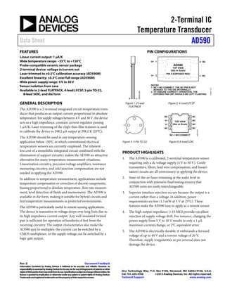
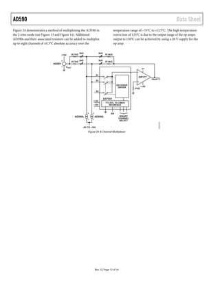
OUTLINE DIMENSIONS
Figure 25. 2-Lead Ceramic Flat Package [FLATPACK]
(F-2)
Dimensions shown in inches and (millimeters)
Figure 26. 3-Pin Metal Header Package [TO-52]
(H-03-1)
Dimensions shown in inches and (millimeters)
0.210 (5.34)
0.200 (5.08)
0.190 (4.83)
0.0065 (0.17)
0.0050 (0.13)
0.0045 (0.12)
0.050 (1.27)
0.041 (1.04)
0.240 (6.10)
0.230 (5.84)
0.220 (5.59)
POSITIVE LEAD
INDICATOR
0.500 (12.69)
MIN
0.093 (2.36)
0.081 (2.06)
0.055 (1.40)
0.050 (1.27)
0.045 (1.14)
0.019 (0.48)
0.017 (0.43)
0.015 (0.38)
0.015 (0.38)
TYP
0.030 (0.76)
TYP
CONTROLLING DIMENSIONS ARE IN INCHES; MILLIMETER DIMENSIONS
(IN PARENTHESES) ARE ROUNDED-OFF INCH EQUIVALENTS FOR
REFERENCE ONLY AND ARE NOT APPROPRIATE FOR USE IN DESIGN.
0.250 (6.35) MIN
0.150 (3.81)
0.115 (2.92)
0.050 (1.27) MAX
0.019 (0.48)
0.016 (0.41)
0.021 (0.53) MAX
0.030 (0.76) MAX
0.195
(4.95)
0.178
(4.52)
0.230
(5.84)
0.209
(5.31)
0.500 (12.70)
MIN
0.046 (1.17)
0.036 (0.91)
0.048 (1.22)
0.028 (0.71)
0.050 (1.27) T.P.
3
1
0.100
(2.54)
T.P.
0.050
(1.27)
T.P.
45° T.P.
2
BASE & SEATING PLANE
022306-A
14. AD590 Data Sheet
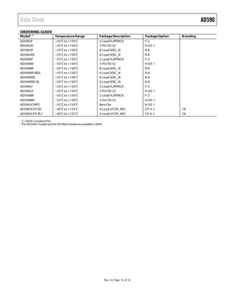
Rev. G | Page 14 of 16
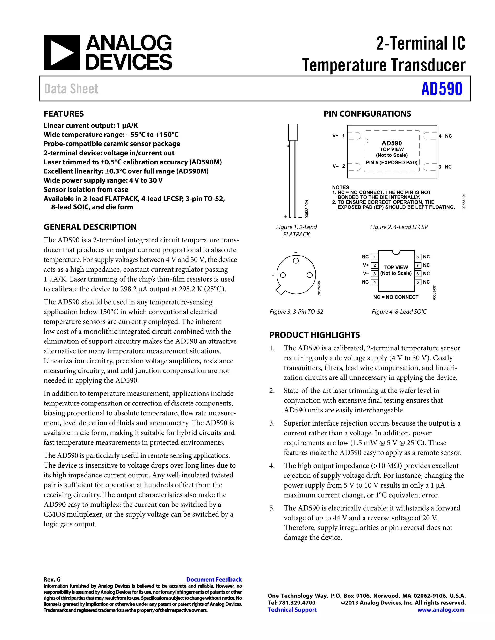
Figure 27. 8-Lead Standard Small Outline Package [SOIC_N]
Narrow Body
(R-8)
Dimensions shown in millimeters and (inches)
Figure 28. 4-Lead Lead Frame Chip Scale Package [LFCSP_WD]
2.00 mm × 3.00 mm Body, Very Very Thin, Dual Lead
(CP-4-1)
Dimensions shown in millimeters
CONTROLLING DIMENSIONS ARE IN MILLIMETERS; INCH DIMENSIONS
(IN PARENTHESES) ARE ROUNDED-OFF MILLIMETER EQUIVALENTS FOR
REFERENCE ONLY AND ARE NOT APPROPRIATE FOR USE IN DESIGN.
COMPLIANT TO JEDEC STANDARDS MS-012-AA
012407-A
0.25 (0.0098)
0.17 (0.0067)
1.27 (0.0500)
0.40 (0.0157)
0.50 (0.0196)
0.25 (0.0099)
45°
8°
0°
1.75 (0.0688)
1.35 (0.0532)
SEATING
PLANE
0.25 (0.0098)
0.10 (0.0040)
4
1
8 5
5.00 (0.1968)
4.80 (0.1890)
4.00 (0.1574)
3.80 (0.1497)
1.27 (0.0500)
BSC
6.20 (0.2441)
5.80 (0.2284)
0.51 (0.0201)
0.31 (0.0122)
COPLANARITY
0.10
1.65
1.55
1.45
0.50
0.40
0.30
TOP VIEW
4
1
3
2
0.35
0.30
0.25
BOTTOM VIEW
PIN 1 INDEX
AREA
SEATING
PLANE
0.80
0.75
0.70
1.80
1.70
1.60
0.203 REF 0.05 MAX
0.00 MIN
0.80 REF
EXPOSED
PAD
PIN 1
INDICATOR
(R 0.15)
FOR PROPER CONNECTION OF
THE EXPOSED PAD, REFER TO
THE PIN CONFIGURATIONS
SECTION OF THIS DATA SHEET.
09-07-2010-B
2.10
2.00
1.90
3.10
3.00
2.90
COMPLIANT TOJEDEC STANDARDS MO-229
COPLANARITY
0.08
0.20 MIN
15. Data Sheet AD590
Rev. G | Page 15 of 16
ORDERING GUIDE
Model1, 2
TemperatureRange PackageDescription PackageOption Branding
AD590JF −55°C to +150°C 2-Lead FLATPACK F-2
AD590JH −55°C to +150°C 3-PinTO-52 H-03-1
AD590JR −55°C to +150°C 8-Lead SOIC_N R-8
AD590JRZ −55°C to +150°C 8-Lead SOIC_N R-8
AD590KF −55°C to +150°C 2-Lead FLATPACK F-2
AD590KH −55°C to +150°C 3-PinTO-52 H-03-1
AD590KR −55°C to +150°C 8-Lead SOIC_N R-8
AD590KR-REEL −55°C to +150°C 8-Lead SOIC_N R-8
AD590KRZ −55°C to +150°C 8-Lead SOIC_N R-8
AD590KRZ-RL −55°C to +150°C 8-Lead SOIC_N R-8
AD590LF −55°C to +150°C 2-Lead FLATPACK F-2
AD590LH −55°C to +150°C 3-PinTO-52 H-03-1
AD590MF −55°C to +150°C 2-Lead FLATPACK F-2
AD590MH −55°C to +150°C 3-PinTO-52 H-03-1
AD590JCHIPS −55°C to +150°C Bare Die H-03-1
AD590JCPZ-R5 −40°C to +125°C 4-Lead LFCSP_WD CP-4-1 7A
AD590JCPZ-RL7 −40°C to +125°C 4-Lead LFCSP_WD CP-4-1 7A
1
Z= RoHS CompliantPart.
2 The AD590xFmodelsandthe AD590xHmodelsare available in883B.