1
1
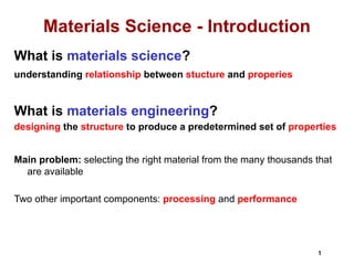
Materials Science -Introduction
What is materials science?
understanding relationship between stucture and properies
What is materials engineering?
designing the structure to produce a predetermined set of properties
Main problem: selecting the right material from the many thousands that
are available
Two other important components: processing and performance
2.
2
2
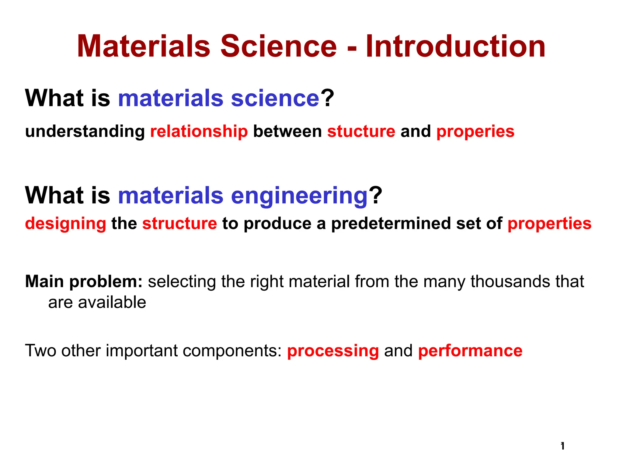
1. Pick ApplicationDetermine required Properties
2. Properties Identify candidate Material(s)
3. Material Identify required Processing
Processing: changes structure and overall shape
ex: casting, sintering, vapor deposition, doping
forming, joining, annealing.
Material: structure, composition.
The Materials Selection Process
3.
3
3
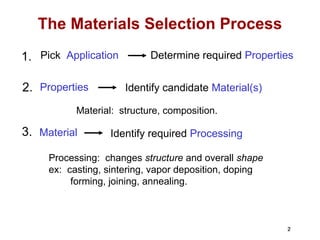
Process-Propery Interaction
Processing
method
Micro-
structure
Property
Engineers makethings. They make them out of materials. The materials
have to support loads, to insulate or conduct heat and electricity, etc.
To make sth. out material you need also a process. Not just any process –
the one you choose has to be compatible with the material you plan to use.
4.
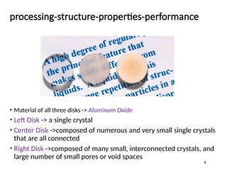
processing-structure-properties-performance
• Material ofall three disks -> Aluminum Oxide
• Left Disk -> a single crystal
• Center Disk ->composed of numerous and very small single crystals
that are all connected
• Right Disk ->composed of many small, interconnected crystals, and
large number of small pores or void spaces
4
5.
5
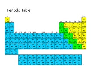
Periodic Table
IA VIIIA
12
H He
1.008 IIA IIIA IVA VA VIA VIIA 4.003
3 4 5 6 7 8 9 10
Li Be B C N O F Ne
6.941 9.012 10.81 12.01 14.01 15.99 19 20.18
11 12 13 14 15 16 17 18
Na Mg Al Si P S Cl Ar
22.99 24.31 IIIB IVB VB VIB VIIB VIIIB IB IIB 26.98 28.09 30.97 32.07 35.45 39.94
19 20 21 22 23 24 25 26 27 28 29 30 31 32 33 34 35 36
K Ca Sc Ti V Cr Mn Fe Co Ni Cu Zn Ga Ge As Se Br Kr
39.1 40.08 44.96 47.88 50.94 52 54.94 55.85 58.93 58.69 63.55 65.39 69.72 72.61 74.92 78.96 79.9 83.8
37 38 39 40 41 42 43 44 45 46 47 48 49 50 51 52 53 54
Rb Sr Y Zr Nb Mo Tc Ru Rh Pd Ag Cd In Sn Sb Te I Xe
85.47 87.62 88.91 91.22 92.91 95.94 -98 101.1 102.9 106.4 107.9 112.4 114.8 118.7 121.8 127.6 126.9 131.3
55 56 57 72 73 74 75 76 77 78 79 80 81 82 83 85 86
Cs Ba La Hf Ta W Re Os Ir Pt Au Hg Tl Pb Bi Po At Rn
132.9 137.3 138.9 178.5 180.9 183.9 186.2 190.2 192.2 195.1 197 200.6 204.4 207.2 209 (209) (210) (222)
87 88 89
Fr Ra Ac
(223) 226 227
58 59 60 61 62 63 64 65 66 67 68 69 70 71
Ce Pr Nd Pm Sm Eu Gd Tb Dy Ho Er Tm Yb Lu
140.1 140.9 144.2 (145) 150.4 152 157.3 158.9 162.5 164.9 167.3 168.9 173 175
90 91 92 93 94 95 96 97 98 99 100 101 102 103
Th Pa U Np Pu Am Cm Bk Cf Es Fm Md No Lr
232 231 238 237 (244) (243) (247) (247) (251) (252) (257) (258) (259) (260)
6.
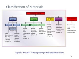
Classification of Materials
FigureI.2 An outline of the engineering materials described in Part I
.
New advanced
materials
Nanomaterials,
shape-memory
alloys
superconductors
semiconductors
…
6
7.
7
7
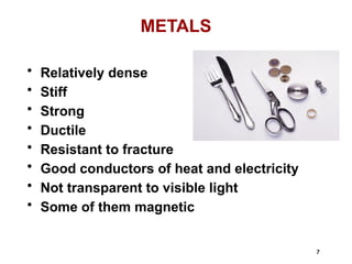
METALS
• Relatively dense
•Stiff
• Strong
• Ductile
• Resistant to fracture
• Good conductors of heat and electricity
• Not transparent to visible light
• Some of them magnetic
8.
9
9
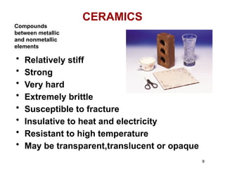
CERAMICS
• Relatively stiff
•Strong
• Very hard
• Extremely brittle
• Susceptible to fracture
• Insulative to heat and electricity
• Resistant to high temperature
• May be transparent,translucent or opaque
Compounds
between metallic
and nonmetallic
elements
9.
10
10
POLYMERS
• Low density
•Not as stiff and strong as metals
• May be ductile
• May be pliable (easily formed into complex
shapes)
• Unreactive in most environments
• Low conductivityofheat and electricity
• Tendency to soften and decomposed with
temperature
10.
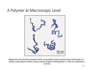
A Polymer atMacroscopic Level
Appearance of real linear polymer chains as recorded using an atomic force microscope on
surface under liquid medium. Chain contour length for this polymer is ~204 nm; thickness is
~0.4 nm
11
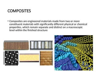
COMPOSITES
• Composites areengineered materials made from two or more
constituent materials with significantly different physical or chemical
properties, which remain separate and distinct on a macroscopic
level within the finished structure
13.
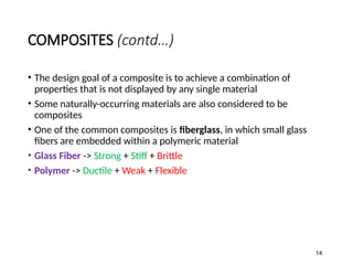
COMPOSITES (contd…)
• Thedesign goal of a composite is to achieve a combination of
properties that is not displayed by any single material
• Some naturally-occurring materials are also considered to be
composites
• One of the common composites is fiberglass, in which small glass
fibers are embedded within a polymeric material
• Glass Fiber -> Strong + Stiff + Brittle
• Polymer -> Ductile + Weak + Flexible
14
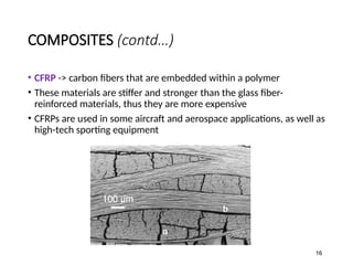
COMPOSITES (contd…)
• CFRP-> carbon fibers that are embedded within a polymer
• These materials are stiffer and stronger than the glass fiber-
reinforced materials, thus they are more expensive
• CFRPs are used in some aircraft and aerospace applications, as well as
high-tech sporting equipment
16
16.
Advanced Materials
• Materialsthat are utilized in high-tech applications
• Hi-Tech -> device or product that operates or functions using
relatively intricate and sophisticated principles
• These advanced materials are typically traditional materials whose
properties have been enhanced, and, also newly developed, high-
performance materials.
• include semiconductors, biomaterials, and materials of the future
(i.e., smart materials and nanoengineered materials)
17
17.
1. Semiconductors
• Semiconductorshave electrical properties that are
intermediate between the conductors (e.g. metals and metal
alloys) and insulators (e.g. ceramics and polymers)
• Common semiconducting materials are crystalline solids but
amorphous and liquid semiconductors are known. These
include hydrogenated amorphous silicon and mixtures of
arsenic, selenium and tellurium in a variety of proportions
• Electrical characteristics are extremely sensitive to the
presence of minute concentrations of impurity atoms
• Semiconductors have caused the advent of integrated
circuitry
18
18.
2. Biomaterials
• Abiomaterial is any material, natural or man-made, that comprises
whole or part of a living structure or biomedical device which
performs, augments, or replaces a natural function
• must not produce toxic substances and must be compatible with
body tissues
• All of the above materials—metals, ceramics, polymers, composites,
and semiconductors—may be used as biomaterials
• Examples -> Artificial hip, bone plates, heart valves, contact lenses,
dental implants, etc
19
19.
Materials of theFuture – Smart Materials
• Smart materials are materials that have one or more properties that
can be significantly changed in a controlled fashion by external
stimuli, such as stress, temperature, moisture, pH, electric or
magnetic fields
• Smart material (or system) include some type of sensor, and an
actuator
• Four types -> shape memory alloys, piezoelectric ceramics,
magnetostrictive materials, and
electrorheological/magnetorheological fluids
20
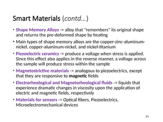
20.
Smart Materials (contd…)
•Shape Memory Alloys -> alloy that "remembers" its original shape
and returns the pre-deformed shape by heating
• Main types of shape memory alloys are the copper-zinc-aluminum-
nickel, copper-aluminum-nickel, and nickel-titanium
• Piezoelectric ceramics -> produce a voltage when stress is applied.
Since this effect also applies in the reverse manner, a voltage across
the sample will produce stress within the sample
• Magnetostrictive materials -> analogous to piezoelectrics, except
that they are responsive to magnetic fields
• Electrorheological and Magnetorheological fluids -> liquids that
experience dramatic changes in viscosity upon the application of
electric and magnetic fields, respectively
• Materials for sensors -> Optical fibers, Piezoelectrics,
Microelectromechanical devices
21
21.
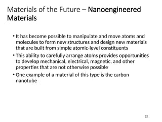
Materials of theFuture – Nanoengineered
Materials
• It has become possible to manipulate and move atoms and
molecules to form new structures and design new materials
that are built from simple atomic-level constituents
• This ability to carefully arrange atoms provides opportunities
to develop mechanical, electrical, magnetic, and other
properties that are not otherwise possible
• One example of a material of this type is the carbon
nanotube
22
22.
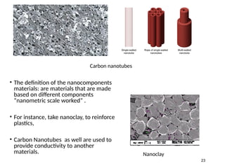
• The definitionof the nanocomponents
materials: are materials that are made
based on different components
“nanometric scale worked” .
• For instance, take nanoclay, to reinforce
plastics,
• Carbon Nanotubes as well are used to
provide conductivity to another
materials.
Carbon nanotubes
Nanoclay
23
25
25
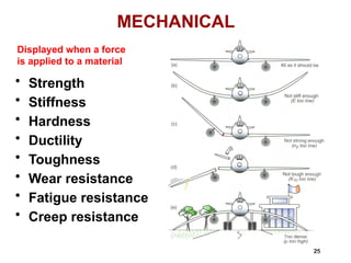
MECHANICAL
• Strength
• Stiffness
•Hardness
• Ductility
• Toughness
• Wear resistance
• Fatigue resistance
• Creep resistance
Displayed when a force
is applied to a material
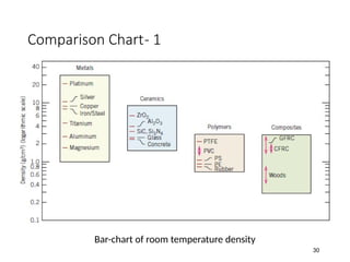
33
33
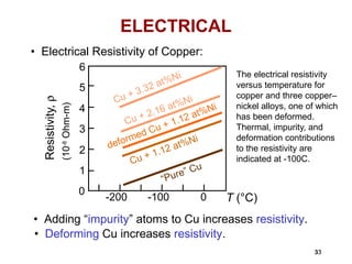
ELECTRICAL
• Electrical Resistivityof Copper:
• Adding “impurity” atoms to Cu increases resistivity.
• Deforming Cu increases resistivity.
The electrical resistivity
versus temperature for
copper and three copper–
nickel alloys, one of which
has been deformed.
Thermal, impurity, and
deformation contributions
to the resistivity are
indicated at -100C.
T (°C)
-200 -100 0
Cu + 3.32 at%Ni
Cu + 2.16 at%Ni
deformed Cu + 1.12 at%Ni
1
2
3
4
5
6
Resistivity,
r
(10
-8
Ohm-m)
0
Cu + 1.12 at%Ni
“Pure” Cu
33.
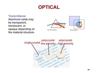
34
34
Transmittance:
Aluminum oxide may
betransparent,
translucent, or
opaque depending on
the material structure.
single crystal
polycrystal:
low porosity
polycrystal:
high porosity
OPTICAL
34.
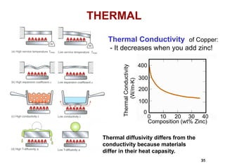
35
35
THERMAL
Thermal Conductivity ofCopper:
- It decreases when you add zinc!
Composition (wt% Zinc)
Thermal
Conductivity
(W/m-K)
400
300
200
100
0
0 10 20 30 40
Thermal diffusivity differs from the
conductivity because materials
differ in their heat capasity.
35.
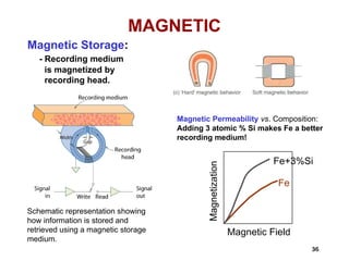
36
36
MAGNETIC
Magnetic Permeability vs.Composition:
Adding 3 atomic % Si makes Fe a better
recording medium!
Schematic representation showing
how information is stored and
retrieved using a magnetic storage
medium.
Magnetic Storage:
- Recording medium
is magnetized by
recording head.
Magnetic Field
Magnetization
Fe+3%Si
Fe
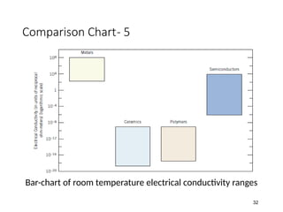
38
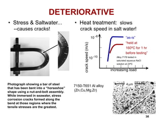
38
DETERIORATIVE
• Stress &Saltwater...
--causes cracks!
Photograph showing a bar of steel
that has been bent into a ‘‘horseshoe’’
shape using a nut-and-bolt assembly.
While immersed in seawater, stress
corrosion cracks formed along the
bend at those regions where the
tensile stresses are the greatest.
4 mm
7150-T651 Al alloy
(Zn,Cu,Mg,Zr)
• Heat treatment: slows
crack speed in salt water!
“held at
160ºC for 1 hr
before testing”
increasing load
crack
speed
(m/s)
“as-is”
10 -10
10 -8
Alloy 7178 tested in
saturated aqueous NaCl
solution at 23ºC
44
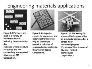
Figure 1.8 Polymersare
used in a variety of
electronic devices,
including these computer
dip
switches, where moisture
resistance and low
conductivity are required.
(Courtesy of CTS
Corporation.)
Figure 1.9 Integrated
circuits for computers and
other electronic devices
rely on the unique
electrical behavior of
semiconducting materials.
(Courtesy of Rogers
Corporation.)
Figure 1.10 The X-wing for
advanced helicopters relies
on a material composed of a
carbon-fiber-
reinforced polymer.
(Courtesy of Sikorsky Aircraft
Division—United
Technologies
Corporation.)
Engineering materials applications
47
47
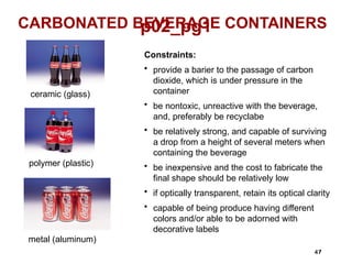
p02_pg1
CARBONATED BEVERAGE CONTAINERS
ceramic(glass)
polymer (plastic)
metal (aluminum)
Constraints:
• provide a barier to the passage of carbon
dioxide, which is under pressure in the
container
• be nontoxic, unreactive with the beverage,
and, preferably be recyclabe
• be relatively strong, and capable of surviving
a drop from a height of several meters when
containing the beverage
• be inexpensive and the cost to fabricate the
final shape should be relatively low
• if optically transparent, retain its optical clarity
• capable of being produce having different
colors and/or able to be adorned with
decorative labels
Editor's Notes
#4 a photograph showing three thin disk specimens placed over some printed matter. It is obvious that the optical properties (i.e., the light transmittance) of each of the three materials are different; the one on the left is transparent (i.e., virtually all of the reflected light passes through it), whereas the disks in the center and on the right are, respectively, translucent (allowing light to pass through diffusely) and opaque.
that is, it is highly perfect—which gives rise to its transparency
… the boundaries between these small crystals scatter a portion of the light reflected from the printed page, which makes this material optically translucent
These pores also effectively scatter the reflected light and render this material opaque
The structures of these three specimens are different in terms of crystal boundaries and pores, which affect the optical transmittance properties. Furthermore, each material was produced using a different processing technique. And, of course, if optical transmittance is an important parameter relative to the ultimate in-service application, the performance of each material will be different.
#11 Y. Roiter and S. Minko, AFM Single Molecule Experiments at the Solid-Liquid Interface: In Situ Conformation of Adsorbed Flexible Polyelectrolyte Chains, Journal of the American Chemical Society, vol. 127, iss. 45, pp. 15688-15689 (2005).
#13 The constituent materials come from the categories discussed above—viz., metals, ceramics, and polymers
LEFT -> Glass/carbon/aramid fibres with thermoset/thermoplastic resins
RIGHT -> single-walled nanotubes (yellow) bundle together when used as the reinforcing element of a composite material. The nanotubes are depicted at the interface with the polymer polyethylene (individual polymer molecules are shown in different shades of blue).
#14 … and also to incorporate the best characteristics of each of the component materials.
… —e.g., wood and bone. However, most of those we consider in our discussions are synthetic (or man-made) composites
… normally an epoxy or polyester. Thus, the resulting fiberglass is relatively stiff, strong, flexible, and ductile. In addition, it has a low density
#16 Another of these technologically important materials is the “carbon fiber reinforced polymer …
.
e.g., bicycles, golf clubs, tennis rackets, and skis/snowboards
#17 2. Examples include electronic equipment (camcorders, CD/DVD players, etc.), computers, fiber-optic systems, spacecraft, aircraft, and military rocketry
3. … they may be of all material types (e.g., metals, ceramics, polymers), and are normally expensive
#18 1. A semiconductor is a material that has an electrical conductivity due to flowing electrons (as opposed to ionic conductivity)
3. … for which the concentrations may be controlled over very small spatial regions.
Amorphous -> without real or apparent crystalline form
4. … that has totally revolutionized the electronics and computer industries (not to mention our lives) over the past three decades.
#19 Biomaterials are employed in components implanted into the human body for replacement of diseased or damaged body parts
… i.e., must not cause adverse biological reactions
#20 that will have a significant influence on many of our technologies. … Term “smart” implies that these materials are able to sense changes in their environments and then respond to these changes in predetermined manners— traits that are also found in living organisms
Sensor (that detects an input signal); Actuator (that performs a responsive and adaptive function)… …. Actuators may be called upon to change shape, position, natural frequency, or mechanical characteristics in response to changes in temperature, electric fields, and/or magnetic fields
#21 metals that, after having been deformed, revert back to their original shapes when temperature is changed … The large deformation results due to martensitic phase change (pseudoelasticity)
.
Piezoelectric ceramics expand and contract in response to an applied electric field (or voltage); conversely, they also generate an electric field when their dimensions are altered
#22 with the advent of scanning probe microscopes, which permit observation of individual atoms and molecules …
the “nano” prefix denotes that the dimensions of these structural entities are on the order of a nanometer (10e-9 m) m)—as a rule, less than 100 nanometers (equivalent to approximately 500 atom diameters)


![Polymer [ बहुलक ] Chemistry Notes PDF - Irfanullah Mehar - JJ Sir Chemistry.pdf](https://cdn.slidesharecdn.com/ss_thumbnails/polymerchemistrynotespdf-irfanullahmehar-jjsirchemistry-260210172118-3f9b37f7-thumbnail.jpg?width=640&height=640&fit=bounds)


