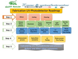
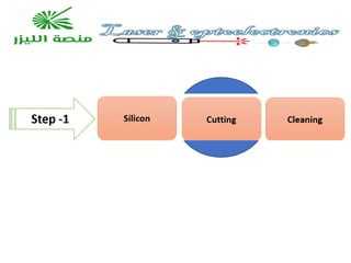
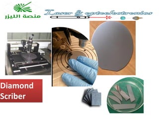
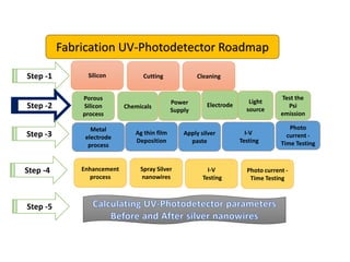
Fabrication UV-Photodetector Roadmap
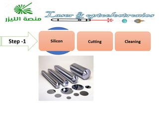
SiliconCutting Cleaning
Step -1
Step -4
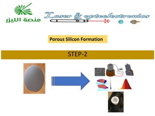
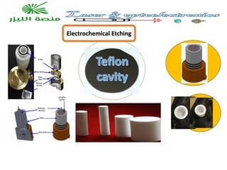
Step -2
Step -3
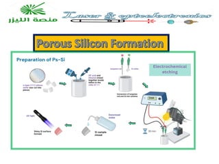
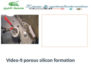
Porous
Silicon
process
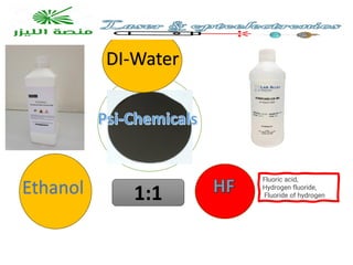
Chemicals
Power
Supply
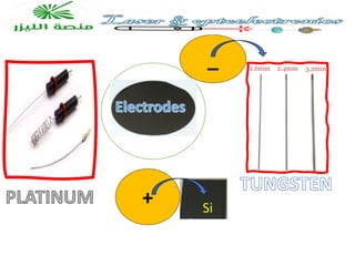
Electrod
e
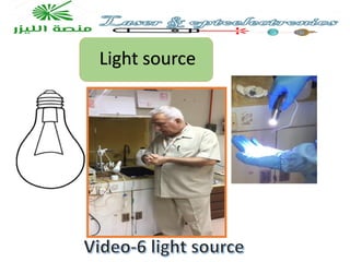
Light
source
Metal
electrode
process
Ag thin film
Deposition
Apply silver
paste
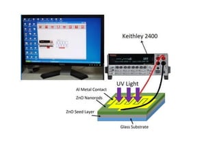
I-V
Testing
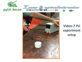
Test the
Psi
emission
Photo
current -
Time Testing
Calculating UV-Photodetector parameters
Before and After silver nanowires
Step -5
Enhancement
process
Spray Silver
nanowires
I-V
Testing
Photo current -
Time Testing
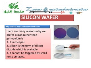
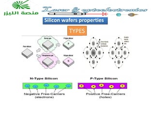
SILICON WAFER
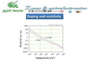
there aremany reasons why we
prefer silicon rather than
germanium is
1. it is cheaper.
2. silicon is the form of silicon
dioxide which is available.
3. it cannot be triggered by small
noise voltages.
Why silicon is most used as semiconductor?
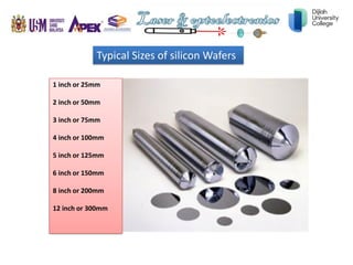
Typical Sizes ofsilicon Wafers
1 inch or 25mm
2 inch or 50mm
3 inch or 75mm
4 inch or 100mm
5 inch or 125mm
6 inch or 150mm
8 inch or 200mm
12 inch or 300mm
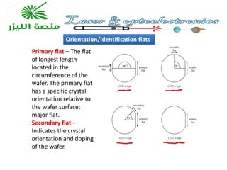
Orientation/identification flats
Primary flat– The flat
of longest length
located in the
circumference of the
wafer. The primary flat
has a specific crystal
orientation relative to
the wafer surface;
major flat.
Secondary flat –
Indicates the crystal
orientation and doping
of the wafer.
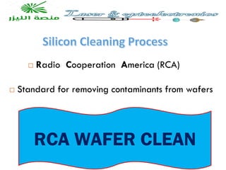
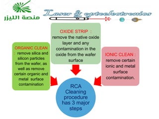
RCA
Cleaning
procedure
has 3 major
steps
ORGANICCLEAN
: remove silica and
silicon particles
from the wafer, as
well as remove
certain organic and
metal surface
contamination
OXIDE STRIP :
remove the native oxide
layer and any
contamination in the
oxide from the wafer
surface
IONIC CLEAN :
remove certain
ionic and metal
surface
contamination.
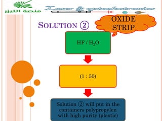
SOLUTION ②
OXIDE
STRIP
HF /H2O
(1 : 50)
Solution ② will put in the
containers polypropylen
with high purity (plastic)
22.
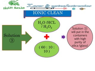
H2O /HCL
/ H2O2
(60 : 10 :
10 )
Solution ③
will put in the
containers
with high
purity of
silica (glass)
IONIC CLEAN
Solution
③
23.
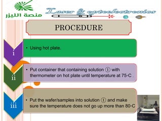
i
• Using hotplate.
ii
• Put container that containing solution ① with
thermometer on hot plate until temperature at 75◦C .
iii
• Put the wafer/samples into solution ① and make
sure the temperature does not go up more than 80◦C
PROCEDURE
24.
PROCEDURE
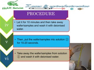
iv
• Let itfor 10 minutes and then take away
wafer/samples and wash it with deionised
water.
v
• Then, put the wafer/samples into solution ②
for 10-20 seconds.
vi
• Take away the wafer/samples from solution
② and wash it with deionised water.
25.
.
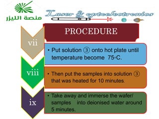
PROCEDURE
vii
• Put solution③ onto hot plate until
temperature become 75◦C.
viii • Then put the samples into solution ③
that was heated for 10 minutes.
ix
• Take away and immerse the wafer/
samples into deionised water around
5 minutes.
Fabrication UV-Photodetector Roadmap
SiliconCutting Cleaning
Step -1
Step -4
Step -2
Step -3
Porous
Silicon
process
Chemicals
Power
Supply
Electrode
Light
source
Metal
electrode
process
Ag thin film
Deposition
Apply silver
paste
I-V
Testing
Test the
Psi
emission
Photo
current -
Time Testing
Calculating UV-Photodetector parameters
Before and After silver nanowires
Step -5
Enhancement
process
Spray Silver
nanowires
I-V
Testing
Photo current -
Time Testing
Technical Notes
1- Don'ttouch
the silicon
surface by your
fingers. keep it
clean
2- Be very
carefully from
the HF acid and
should wearing
the safety
clothes
3- Don’t dip the
crocodile clamp
touch the
solution during
conducting the
experiment
4- connecte the
silicon sample
very well
5- always clean
the tungsten
wire using sand
paper.
46.
Technical Notes
9-Before testthe
silicon try to clean the
sample using DI Water
and dry the sample
using hair dryer
6-Don’t let the
crocodile clamp
terminals touch
each other during
the power supply
functioning
7- Increase the
voltage slowly to
avoid flowing high
current inside the
solution
8- Fix the time
properly to get
same results
47.
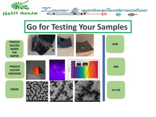
Go for TestingYour Samples
POROUS
SILICON
EMISSION
POROUS
SILICON
INSIDE
THE
WATER
FESEM UV-VIS
XRD
AFM
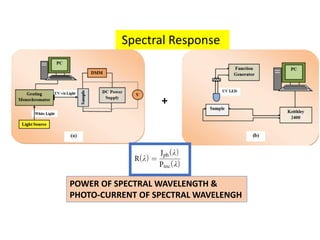
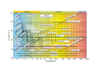
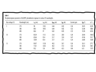
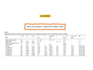
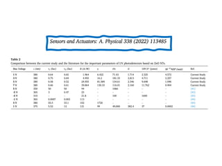
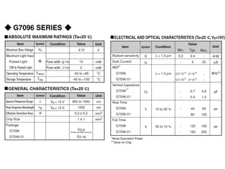
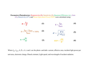
Parameters Photodetector: Responsivity(R), Sensitivity (S), Quantum Efficiency (η) , Gain
(G), Detectivity (D*), and Noise Equivalent Power (NEP) were calculated using:
𝑹 =
𝑰𝒑𝒉
𝑷
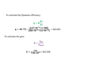
𝜼 = 𝑹
𝒉𝒄
𝝀𝒆
𝑺 =
𝑰𝒑𝒉 − 𝑰𝒅𝒂𝒓𝒌
𝑰𝒅𝒂𝒓𝒌
⨯ 100%
𝑮 =
𝑰𝒑𝒉
𝑰𝒅𝒂𝒓𝒌
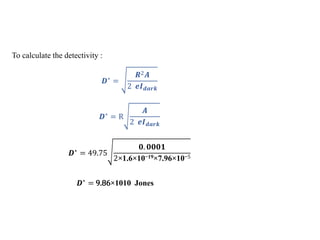
𝑫∗
=
𝑹2𝑨
2 𝒆𝑰𝒅𝒂𝒓𝒌
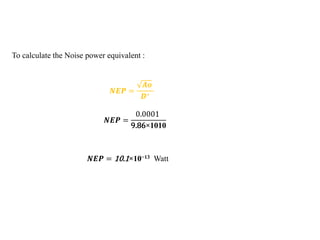
𝑵𝑬𝑷 =
𝑨𝒐
𝑫∗
(1)
(2)
(3)
(4)
(5)
(6)
Where Iph, Idark, A, P, e, h, c and λ are the photo- and dark- current, effective area, incident light power per
unit area, electronic charge, Planck constant, Light speed, and wavelength of incident radiation.
67.
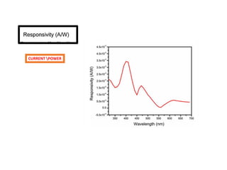
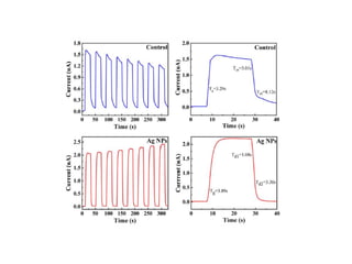
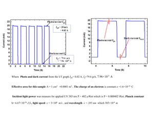
Where Photo anddark current from the I-T graph Iph= 0.02 A, Id=79.6 µA, 7.96×10⁻⁵ A
Effective area for this sample A = 1 cm2 =0.0001 m2 , The charge of an electron is constant e =1.6×10⁻¹⁹ C
Incident light power was measure for applied UV 385 nm P = 402 µWatt which is P = 0.000402 Watt, Planck constant
h= 6.67×10⁻³⁴ J.S , light speed c = 3×10⁸ m/s , and wavelength λ = 385 nm which 385×10-9 m
68.
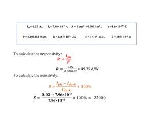
Iph= 0.02 A,Id= 7.96×10⁻⁵ A A = 1 cm2 =0.0001 m2 , e =1.6×10⁻¹⁹ C
P = 0.000402 Watt, h = 6.67×10⁻³⁴ J.S , c = 3×10⁸ m/s , λ = 385×10-9 m
To calculate the responsivity:
𝑹 =
𝑰𝒑𝒉
𝑷
𝑹 =
0.02
0.000402
= 49.75 A/W
𝑺 =
𝑰𝒑𝒉 − 𝑰𝒅𝒂𝒓𝒌
𝑰𝒅𝒂𝒓𝒌
⨯ 100%
𝑺 =
𝟎. 𝟎𝟐 − 7.96×10⁻⁵
7.96×10−5
⨯ 100% = 25000
To calculate the sensitivity: