Lecture 03
Basic AmplifierStages / Cascode Amplifier
This is a modified version of Dr Hesham’s Lectures
Dr. Hesham A. Omran
Analog IC Design
ً
يلِ
لَق ا
َّلِ
إِ
مْلِ
عْلا َ
نِ
م ْمُ
يتِ
توُأاَ
مَ
و
11 March 2022 8
شعبان
1443
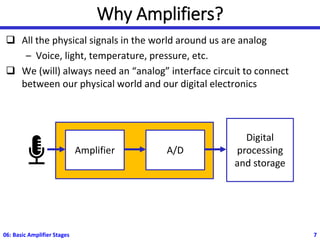
Why Amplifiers?
❑ Allthe physical signals in the world around us are analog
– Voice, light, temperature, pressure, etc.
❑ We (will) always need an “analog” interface circuit to connect
between our physical world and our digital electronics
06: Basic Amplifier Stages 7
Amplifier A/D
Digital
processing
and storage
8.
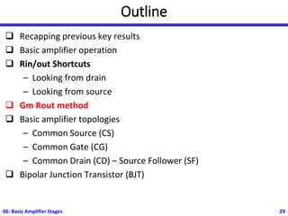
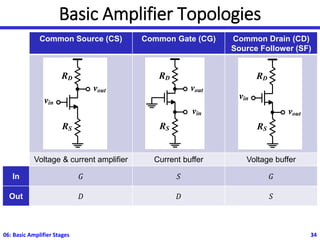
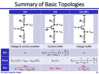
Basic Amplifier Topologies
CommonSource (CS) Common Gate (CG) Common Drain (CD)
Source Follower (SF)
Voltage & current amplifier Current buffer Voltage buffer
In 𝐺 𝑆 𝐺
Out 𝐷 𝐷 𝑆
06: Basic Amplifier Stages 8
RD
vout
vin
RS
RD
vin
RS
vout
RD
vout
vin
RS
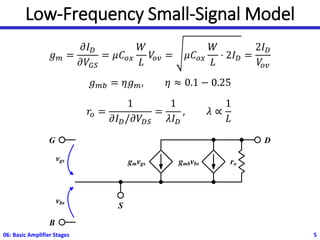
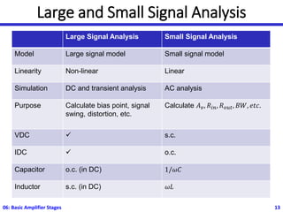
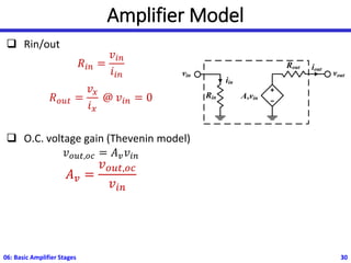
Large and SmallSignal Analysis
Large Signal Analysis Small Signal Analysis
Model Large signal model Small signal model
Linearity Non-linear Linear
Simulation DC and transient analysis AC analysis
Purpose Calculate bias point, signal
swing, distortion, etc.
Calculate 𝐴𝑣, 𝑅𝑖𝑛, 𝑅𝑜𝑢𝑡, 𝐵𝑊, 𝑒𝑡𝑐.
VDC ✓ s.c.
IDC ✓ o.c.
Capacitor o.c. (in DC) 1/𝜔𝐶
Inductor s.c. (in DC) 𝜔𝐿
06: Basic Amplifier Stages 13
14.
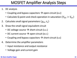
MOSFET Amplifier AnalysisSteps
1. DC analysis
• Coupling and bypass capacitors → open-circuit (o.c)
• Calculate Q-point and check operation in saturation 𝑉𝐷𝑆 > 𝑉
𝑜𝑣
2. Calculate small signal parameters 𝑔𝑚, 𝑟𝑜
3. Draw the small signal equivalent circuit
• DC voltage source → short-circuit (s.c.)
• DC current source → open-circuit (o.c.)
• Coupling and bypass capacitors → short-circuit (s.c)
4. Determine the amplifier parameters
• Input resistance and output resistance
• Voltage gain and current gain
06: Basic Amplifier Stages 14
15.
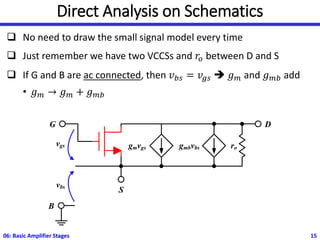
Direct Analysis onSchematics
❑ No need to draw the small signal model every time
❑ Just remember we have two VCCSs and 𝑟𝑜 between D and S
❑ If G and B are ac connected, then 𝑣𝑏𝑠 = 𝑣𝑔𝑠 ➔ 𝑔𝑚 and 𝑔𝑚𝑏 add
• 𝑔𝑚 → 𝑔𝑚 + 𝑔𝑚𝑏
06: Basic Amplifier Stages 15
gmvgs ro
gmbvbs
G D
S
vbs
vgs
B
16.
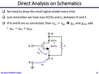
Direct Analysis onSchematics
❑ No need to draw the small signal model every time
❑ Just remember we have two VCCSs and 𝑟𝑜 between D and S
❑ If G and B are ac connected, then 𝑣𝑏𝑠 = 𝑣𝑔𝑠 ➔ 𝑔𝑚 and 𝑔𝑚𝑏 add
• 𝑔𝑚 → 𝑔𝑚 + 𝑔𝑚𝑏
06: Basic Amplifier Stages 16
gmvgs
+
gmbvbs ro
B
vgs
S
G
D
vbs
17.
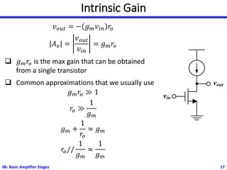
Intrinsic Gain
𝑣𝑜𝑢𝑡 =− 𝑔𝑚𝑣𝑖𝑛 𝑟𝑜
|𝐴𝑣| =
𝑣𝑜𝑢𝑡
𝑣𝑖𝑛
= 𝑔𝑚𝑟𝑜
❑ 𝑔𝑚𝑟𝑜 is the max gain that can be obtained
from a single transistor
❑ Common approximations that we usually use
𝑔𝑚𝑟𝑜 ≫ 1
𝑟𝑜 ≫
1
𝑔𝑚
𝑔𝑚 +
1
𝑟𝑜
≈ 𝑔𝑚
𝑟𝑜//
1
𝑔𝑚
≈
1
𝑔𝑚
06: Basic Amplifier Stages 17
vin
vout
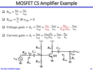
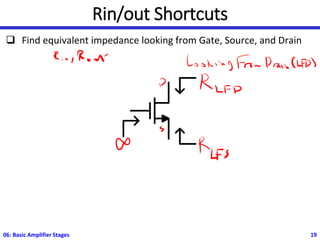
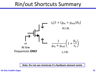
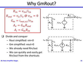
Rin/out Shortcuts
❑ Findequivalent impedance looking from Gate, Source, and Drain
06: Basic Amplifier Stages 19
20.
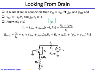
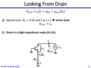
Looking From Drain
❑If G and B are ac connected, then 𝑣𝑏𝑠 = 𝑣𝑔𝑠 ➔ 𝑔𝑚 and 𝑔𝑚𝑏 add
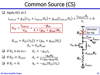
❑ 𝑣𝑔𝑠 = −𝑖𝑥𝑅𝑆 and 𝑔𝑚𝑟𝑜 ≫ 1
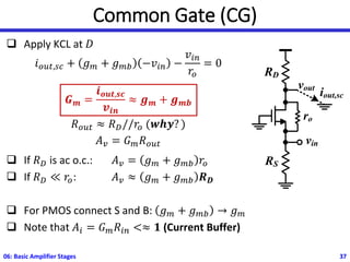
❑ Apply KCL at 𝐷
𝑖𝑥 = 𝑔𝑚 + 𝑔𝑚𝑏 −𝑖𝑥𝑅𝑆 +
𝑣𝑥 − 𝑖𝑥𝑅𝑆
𝑟𝑜
𝑅𝐿𝐹𝐷 =
𝑣𝑥
𝑖𝑥
= 𝑟𝑜 + 𝑔𝑚 + 𝑔𝑚𝑏 𝑟𝑜𝑅𝑆 + 𝑅𝑆 ≈ 𝑟𝑜 1 + 𝑔𝑚 + 𝑔𝑚𝑏 𝑅𝑆
06: Basic Amplifier Stages 20
RS
vx
RLFD
ix
ixRS
ix
ro
vgs
21.
Looking From Drain
𝑅𝐿𝐹𝐷≈ 𝑟𝑜 1 + 𝑔𝑚 + 𝑔𝑚𝑏 𝑅𝑆
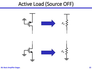
❑ Special case: 𝑅𝑆 = 0 (G and S ac s.c.) ➔ active load
𝑅𝐿𝐹𝐷 ≈ 𝑟𝑜
❑ Drain is a high-impedance node (H.I.N.)
06: Basic Amplifier Stages 21
RS
vx
RLFD
ix
ixRS
ix
ro
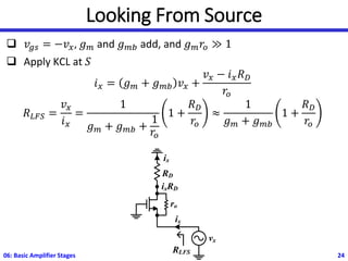
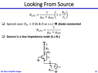
Looking From Source
𝑅𝐿𝐹𝑆≈
1
𝑔𝑚 + 𝑔𝑚𝑏
1 +
𝑅𝐷
𝑟𝑜
❑ Special case: 𝑅𝐷 = 0 (G & D ac s.c.) ➔ diode connected
𝑅𝐿𝐹𝑆 ≈
1
𝑔𝑚 + 𝑔𝑚𝑏
❑ Source is a low impedance node (L.I.N.)
06: Basic Amplifier Stages 25
vx
RLFS
ix
RD
ixRD
ix
ro
26.
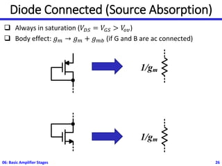
Diode Connected (SourceAbsorption)
❑ Always in saturation (𝑉𝐷𝑆 = 𝑉𝐺𝑆 > 𝑉
𝑜𝑣)
❑ Body effect: 𝑔𝑚 → 𝑔𝑚 + 𝑔𝑚𝑏 (if G and B are ac connected)
06: Basic Amplifier Stages 26
1/gm
1/gm
27.
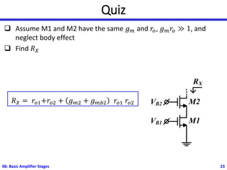
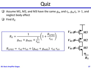
Quiz
❑ Assume M1,M2, and M3 have the same 𝑔𝑚 and 𝑟𝑜, 𝑔𝑚𝑟𝑜 ≫ 1, and
neglect body effect
❑ Find 𝑅𝑋
06: Basic Amplifier Stages 27
VB1
VB2
RX
M2
M1
VB3 M3
𝑅𝑋 =
1
𝑔𝑚1 + 𝑔𝑚𝑏1 +
1
𝑟𝑜1
1 +
𝑅𝐿𝐹𝐷2
𝑟𝑜1
𝑅𝐿𝐹𝐷2 = 𝑟𝑜2+𝑟𝑜3 + 𝑔𝑚2 + 𝑔𝑚𝑏2 𝑟𝑜2 𝑟𝑜3
28.
Rin/out Shortcuts Summary
06:Basic Amplifier Stages 28
1
𝑔𝑚 + 𝑔𝑚𝑏
1 +
𝑅𝐷
𝑟𝑜
L.I.N.
𝑟𝑜 1 + 𝑔𝑚 + 𝑔𝑚𝑏 𝑅𝑆
H.I.N.
∞
At low
frequencies ONLY
Note: Do not use shortcuts if a feedback element exists
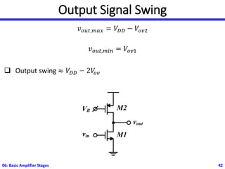
Quiz
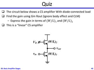
❑ The circuitbelow shows a CS amplifier With diode-connected load
❑ Find the gain using Gm Rout (ignore body effect and CLM)
– Express the gain in terms of (𝑊/𝐿)1 and (𝑊/𝐿)2
❑ This is a “linear” CS amplifier
06: Basic Amplifier Stages 40
VB
(W/L)1
(W/L)2
vin
vout
41.
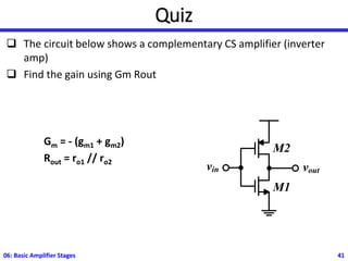
Quiz
❑ The circuitbelow shows a complementary CS amplifier (inverter
amp)
❑ Find the gain using Gm Rout
Gm = - (gm1 + gm2)
Rout = ro1 // ro2
06: Basic Amplifier Stages 41
M1
M2
vin vout
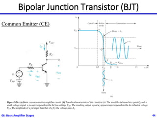
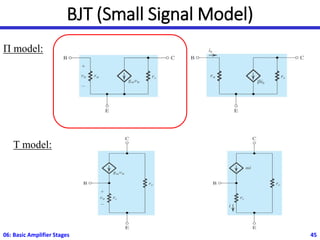
Bipolar Junction Transistor(BJT)
06: Basic Amplifier Stages 44
Figure 5.26 (a) Basic common-emitter amplifier circuit. (b) Transfer characteristic of the circuit in (a). The amplifier is biased at a point Q, and a
small voltage signal vi is superimposed on the dc bias voltage VBE. The resulting output signal vo appears superimposed on the dc collector voltage
VCE. The amplitude of vo is larger than that of vi by the voltage gain Av.
Common Emitter (CE)
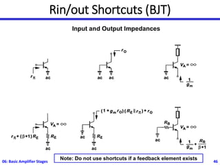
Rin/out Shortcuts (BJT)
06:Basic Amplifier Stages 46
Note: Do not use shortcuts if a feedback element exists
47.
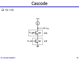
Lecture 3 part2
Cascode Amplifiers
Integrated Circuits Lab (ICL)
Electronics and Communications Eng. Dept.
Faculty of Engineering
Ain Shams University
Dr. Hesham A. Omran
Analog IC Design
ً
يلِ
لَق ا
َّلِ
إِ
مْلِ
عْلا َ
نِ
م ْمُ
يتِ
توُأاَ
مَ
و
11 March 2022 8
شعبان
1443
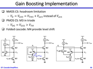
48.
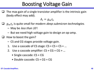
Boosting Voltage Gain
❑The max gain of a single transistor amplifier is the intrinsic gain
(body effect may add).
𝐴𝑖 = 𝑔𝑚𝑟𝑜
❑ 𝑔𝑚𝑟𝑜 is quite small for modern deep submicron technologies.
– May be less than 10 !
– But we need high voltage gain to design an op-amp.
❑ How to boost the gain?
– CS and CG stages provide voltage gain.
1. Use a cascade of CS stage: CS + CS + CS + …
2. Use a cascode amplifier: CS + CG + CG + …
• Single cascode: CS + CG
• Double cascode: CS + CG + CG
07: Cascode Amplifiers 48
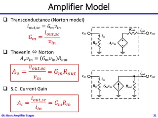
Cascode Gain UsingGmRout
❑ Transconductance is always related
to the input transistor (VCCS)
𝑖𝑜𝑢𝑡,𝑠𝑐 ≈ −𝑔𝑚1𝑣𝑖𝑛
𝐺𝑚 =
𝑖𝑜𝑢𝑡,𝑠𝑐
𝑣𝑖𝑛
≈ −𝑔𝑚1
Same Gm of CS
𝑅𝑜𝑢𝑡 ≈ 𝑟𝑜2 1 + 𝑔𝑚2 + 𝑔𝑚𝑏2 𝑟𝑜1
≈ 𝑟𝑜2 𝑔𝑚2 + 𝑔𝑚𝑏2 𝑟𝑜1
Rout significantly boosted
𝐴𝑣 ≈ −𝑔𝑚1𝑟𝑜1 𝑔𝑚2 + 𝑔𝑚𝑏2 𝑟𝑜2
❑ Assume all 𝑔𝑚 and 𝑟𝑜 are equal and
neglect body effect
𝐴𝑣 = − 𝑔𝑚𝑟𝑜
2
07: Cascode Amplifiers 50
vout
VB
vin M1
M2
iout,sc
iout,sc
51.
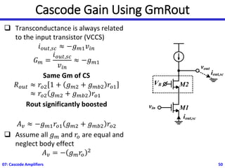
Cascode as CS+ CG
𝐶𝑆:
𝑣𝑥
𝑣𝑖𝑛
= −𝑔𝑚1 𝑟𝑜1//∞
𝐶𝐺:
𝑣𝑜𝑢𝑡
𝑣𝑥
= 𝑔𝑚2 + 𝑔𝑚𝑏2 𝑟𝑜2
𝐴𝑣 =
𝑣𝑥
𝑣𝑖𝑛
⋅
𝑣𝑜𝑢𝑡
𝑣𝑥
≈ −𝑔𝑚1𝑟𝑜1 𝑔𝑚2 + 𝑔𝑚𝑏2 𝑟𝑜2
❑ Assume all 𝑔𝑚 and 𝑟𝑜 are equal and
neglect body effect
𝐴𝑣 = − 𝑔𝑚𝑟𝑜
2
07: Cascode Amplifiers 51
vout
VB
vin M1
M2
CS
CG
vx
52.
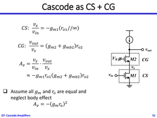
Quiz
❑ The circuitbelow shows a double cascode.
❑ Find the voltage gain. Assume all 𝑔𝑚 and 𝑟𝑜 are equal and neglect
body effect.
07: Cascode Amplifiers 52
vout
VB1
vin M1
M2
VB2 M3
53.
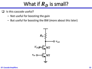
What if 𝑹𝑫is small?
❑ Is this cascode useful?
– Not useful for boosting the gain
– But useful for boosting the BW (more about this later)
07: Cascode Amplifiers 53
vout
VB
vin M1
M2
RD
54.
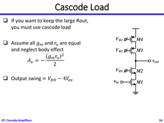
Cascode Load
❑ Ifyou want to keep the large Rout,
you must use cascode load
❑ Assume all 𝑔𝑚 and 𝑟𝑜 are equal
and neglect body effect
𝐴𝑣 = −
𝑔𝑚𝑟𝑜
2
2
❑ Output swing ≈ 𝑉𝐷𝐷 − 4𝑉
𝑜𝑣
07: Cascode Amplifiers 54
vout
VB1
vin M1
M2
VB2
VB3
M3
M4
55.
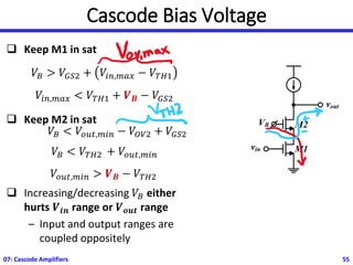
Cascode Bias Voltage
❑Keep M1 in sat
𝑉𝐵 > 𝑉𝐺𝑆2 + 𝑉𝑖𝑛,𝑚𝑎𝑥 − 𝑉𝑇𝐻1
𝑉𝑖𝑛,𝑚𝑎𝑥 < 𝑉𝑇𝐻1 + 𝑽𝑩 − 𝑉𝐺𝑆2
❑ Keep M2 in sat
𝑉𝐵 < 𝑉𝑇𝐻2 + 𝑉𝑜𝑢𝑡,𝑚𝑖𝑛
𝑉𝑜𝑢𝑡,𝑚𝑖𝑛 > 𝑽𝑩 − 𝑉𝑇𝐻2
❑ Increasing/decreasing 𝑉𝐵 either
hurts 𝑽𝒊𝒏 range or 𝑽𝒐𝒖𝒕 range
– Input and output ranges are
coupled oppositely
07: Cascode Amplifiers 55
vout
VB
vin M1
M2
𝑉𝐵 < 𝑉𝑜𝑢𝑡,𝑚𝑖𝑛 − 𝑉𝑂𝑉2 + 𝑉𝐺𝑆2
56.
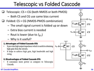
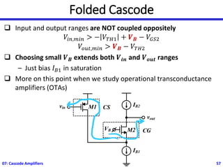
Telescopic vs FoldedCascode
❑ Telescopic: CS + CG (both NMOS or both PMOS)
– Both CS and CG use same bias current
❑ Folded: CS + CG (NMOS-PMOS combination)
– The small signal current is folded up or down
– Extra bias current is needed
– Rout is lower (due to 𝐼𝐵1)
– Why is it useful?
07: Cascode Amplifiers 56
vout
VB
vin M1
M2
CS
CG
vout
VB M2
CS
CG
vin M1
IB1
IB2
57.
Folded Cascode
❑ Inputand output ranges are NOT coupled oppositely
𝑉𝑖𝑛,𝑚𝑖𝑛 > − 𝑉𝑇𝐻1 + 𝑽𝑩 − 𝑉𝐺𝑆2
𝑉𝑜𝑢𝑡,𝑚𝑖𝑛 > 𝑽𝑩 − 𝑉𝑇𝐻2
❑ Choosing small 𝑽𝑩 extends both 𝑽𝒊𝒏 and 𝑽𝒐𝒖𝒕 ranges
– Just bias 𝐼𝐵1 in saturation
❑ More on this point when we study operational transconductance
amplifiers (OTAs)
07: Cascode Amplifiers 57
vout
VB M2
CS
CG
vin M1
IB1
IB2
58.
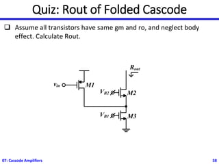
Quiz: Rout ofFolded Cascode
❑ Assume all transistors have same gm and ro, and neglect body
effect. Calculate Rout.
07: Cascode Amplifiers 58
VB2 M2
vin M1
VB1
Rout
M3
59.
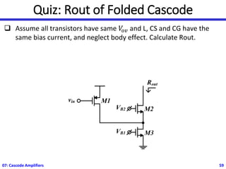
Quiz: Rout ofFolded Cascode
❑ Assume all transistors have same 𝑉
𝑜𝑣 and L, CS and CG have the
same bias current, and neglect body effect. Calculate Rout.
07: Cascode Amplifiers 59
VB2 M2
vin M1
VB1
Rout
M3
60.
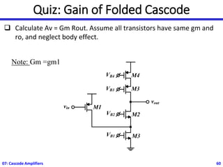
Quiz: Gain ofFolded Cascode
❑ Calculate Av = Gm Rout. Assume all transistors have same gm and
ro, and neglect body effect.
07: Cascode Amplifiers 60
VB2 M2
vin M1
VB1 M3
vout
VB3
VB4
M3
M4
Note: Gm =gm1
References
❑ A. Sedraand K. Smith, “Microelectronic Circuits,” Oxford University
Press, 7th ed., 2015
❑ B. Razavi, “Fundamentals of Microelectronics,” Wiley, 2nd ed., 2014
❑ B. Razavi, “Design Of Analog CMOS Integrated Circuit,” McGraw-
Hill, 2nd ed., 2017
62
07: Cascode Amplifiers
63.
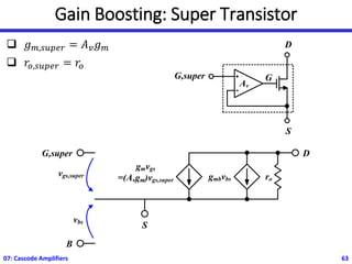
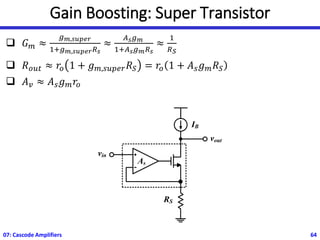
Gain Boosting: SuperTransistor
❑ 𝑔𝑚,𝑠𝑢𝑝𝑒𝑟 = 𝐴𝑣𝑔𝑚
❑ 𝑟𝑜,𝑠𝑢𝑝𝑒𝑟 = 𝑟𝑜
07: Cascode Amplifiers 63
G,super
S
D
Av
G
gmvgs
=(Avgm)vgs,super ro
gmbvbs
G,super D
S
B
vgs,super
vbs
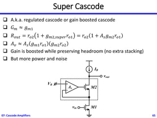
Super Cascode
❑ A.k.a.regulated cascode or gain boosted cascode
❑ 𝐺𝑚 ≈ 𝑔𝑚1
❑ 𝑅𝑜𝑢𝑡 = 𝑟𝑜2 1 + 𝑔𝑚2,𝑠𝑢𝑝𝑒𝑟𝑟𝑜1 = 𝑟𝑜2 1 + 𝐴𝑠𝑔𝑚2𝑟𝑜1
❑ 𝐴𝑣 ≈ 𝐴𝑠 𝑔𝑚1𝑟𝑜1 𝑔𝑚2𝑟𝑜2
❑ Gain is boosted while preserving headroom (no extra stacking)
❑ But more power and noise
07: Cascode Amplifiers 65
As
IB
vout
vin
VB
M1
M2


![MOSFET CS Amplifier Example
06: Basic Amplifier Stages 9
[Sedra/Smith, 2015]](https://image.slidesharecdn.com/lec3newbasicamplifiers-250224004057-ef4fafd3/85/LEC-3-New-basic_amplifiers-pdffffffffffffffffff-9-320.jpg)
![MOSFET CS Amplifier Example
06: Basic Amplifier Stages 10
[Sedra/Smith, 2015]](https://image.slidesharecdn.com/lec3newbasicamplifiers-250224004057-ef4fafd3/85/LEC-3-New-basic_amplifiers-pdffffffffffffffffff-10-320.jpg)
![MOSFET CS Amplifier Example
06: Basic Amplifier Stages 11
[Sedra/Smith, 2015]](https://image.slidesharecdn.com/lec3newbasicamplifiers-250224004057-ef4fafd3/85/LEC-3-New-basic_amplifiers-pdffffffffffffffffff-11-320.jpg)


![Filtering Antenna[1] - Read-Only (2).pptx](https://cdn.slidesharecdn.com/ss_thumbnails/filteringantenna1-read-only2-250520164908-7b67a423-thumbnail.jpg?width=640&height=640&fit=bounds)


